Practical case: Water tank level control

Water tank level control prototype (Maker Style)

Level: Basic. Implement a logic safety stop for a water pump using a NAND gate.

Objective and use case

In this session, you will build a digital safety circuit using a 74HC00 NAND gate. The circuit monitors two liquid level sensors and automatically cuts power to a «pump» (simulated by an LED) only when both sensors indicate the tank is dangerously full.

  • Industrial tank filling: Prevents chemical spills by ensuring redundant sensors must agree before triggering an emergency shutdown.
  • Sump pump systems: Prevents motor burnout or overflow by managing logic states between high-water and critical-overflow marks.
  • Home automation: Simple logic for reservoir management without needing a microcontroller.

Expected outcome:
* Normal Operation: The LED (pump) remains ON (Logic High, ~5 V) when the tank is empty or partially full.
* Emergency Stop: The LED turns OFF (Logic Low, ~0 V) immediately when both switch inputs are Logic High (simulating water detection).
* Validation: A specific Truth Table will be verified where only the input condition 1, 1 results in an output of 0.

Target audience: Basic level electronics students and hobbyists.

Materials

  • V1: 5 V DC power supply, function: Main circuit power.
  • U1: 74HC00, function: Quad 2-Input NAND Gate IC.
  • S1: SPST Toggle Switch, function: High Level Sensor simulator.
  • S2: SPST Toggle Switch, function: Safety Level Sensor simulator.
  • R1: 10 kΩ resistor, function: Pull-down for S1.
  • R2: 10 kΩ resistor, function: Pull-down for S2.
  • R3: 330 Ω resistor, function: Current limiting for the Pump Status LED.
  • D1: Green LED, function: Pump status indicator (ON = Running, OFF = Stopped).

Pin-out of the IC used

Chip: 74HC00 (Quad 2-Input NAND Gate)

Pin Name Logic function Connection in this case
1 1 A Input A Connected to Sensor S1
2 1B Input B Connected to Sensor S2
3 1Y Output Y Connected to LED (Pump)
7 GND Ground Connected to 0 V
14 VCC Power Connected to 5 V

Wiring guide

Construct the circuit following these node connections. Ensure the power supply is off while building.

  • Power Rail: Connect V1 positive terminal to node VCC and negative terminal to node 0 (GND).
  • IC Power: Connect U1 pin 14 to VCC and pin 7 to 0.
  • Sensor 1 (Input A):
    • Connect S1 between VCC and node SENSOR_HI.
    • Connect R1 between SENSOR_HI and 0 (Pull-down).
    • Connect U1 pin 1 to node SENSOR_HI.
  • Sensor 2 (Input B):
    • Connect S2 between VCC and node SENSOR_SAFE.
    • Connect R2 between SENSOR_SAFE and 0 (Pull-down).
    • Connect U1 pin 2 to node SENSOR_SAFE.
  • Pump Control (Output):
    • Connect U1 pin 3 to node PUMP_CTRL.
    • Connect D1 (Anode) to node PUMP_CTRL.
    • Connect D1 (Cathode) to node LED_NODE.
    • Connect R3 between LED_NODE and 0.

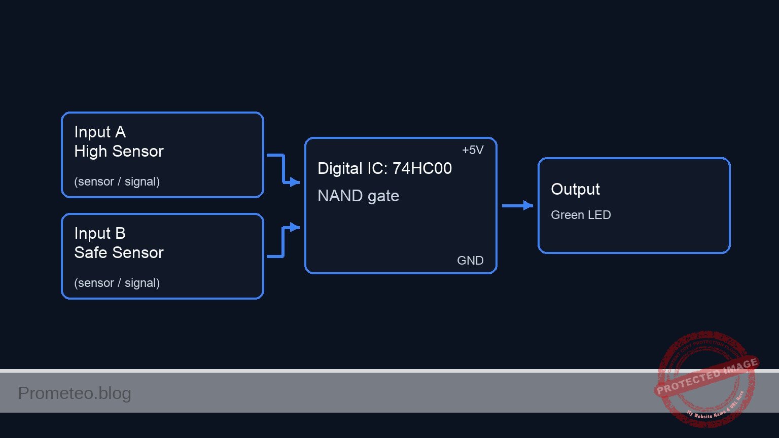
Conceptual block diagram

Conceptual block diagram — 74HC00 NAND gate
Quick read: inputs → main block → output (actuator or measurement). This summarizes the ASCII schematic below.

Schematic

Title: Practical case: Water tank level control

      INPUTS (Sensors)                       PROCESSING (U1: 74HC00)                  OUTPUT (Pump Indicator)
   ======================                  ===========================              ===========================

   [ VCC ]
      |
   [ S1: High Sensor ]
      |
      +--(Node: SENSOR_HI)---------------> [ U1: Pin 1 (Input A) ]
      |                                             |
   [ R1: 10k Pull-Down ]                            |
      |                                             v
   [ GND ]                                     [ NAND Gate ] --(Node: PUMP_CTRL)--> [ D1: Green LED ]
                                                    ^                                       |
                                                    |                               (Node: LED_NODE)
   [ VCC ]                                          |                                       |
      |                                             |                                  [ R3: 330R ]
   [ S2: Safe Sensor ]                              |                                       |
      |                                             |                                    [ GND ]
      +--(Node: SENSOR_SAFE)-------------> [ U1: Pin 2 (Input B) ]
      |
   [ R2: 10k Pull-Down ]
      |
   [ GND ]

   (Note: U1 Power Connections -> Pin 14: VCC, Pin 7: GND)
Electrical Schematic

Electrical diagram

Electrical diagram for case: Water tank level control
Generated from the validated SPICE netlist for this case.

🔒 This electrical diagram is premium. With the monthly membership (7-day free trial) you can unlock the complete didactic material and the print-ready PDF pack.🔓 See premium access plans

Truth table

The 74HC00 acts as a safety interlock. The pump runs (Output 1) by default and only stops (Output 0) when the specific danger condition (1, 1) is met.

S1 (High Level) S2 (Safety Level) Voltage at Pin 3 Pump Status (LED) Logic State
0 (Dry) 0 (Dry) High (~5 V) ON Safe
0 (Dry) 1 (Wet) High (~5 V) ON Sensor Error/Safe
1 (Wet) 0 (Dry) High (~5 V) ON Warning Level
1 (Wet) 1 (Wet) Low (~0 V) OFF STOP (Danger)

Measurements and tests

  1. Default State Check: Ensure S1 and S2 are open (OFF). Power on the circuit. Measure the voltage at node PUMP_CTRL relative to GND. It should read approximately 5 V. The Green LED should be lit.
  2. Single Sensor Test: Close S1 only. The LED should remain ON. Open S1 and close S2 only. The LED should remain ON.
  3. Safety Stop Test: Close both S1 and S2 simultaneously.
    • Measure the voltage at node PUMP_CTRL. It should drop to near 0 V (< 0.1 V).
    • Confirm the LED turns OFF immediately.
  4. Recovery: Open either switch; the LED should turn back ON.

SPICE netlist and simulation

Reference SPICE Netlist (ngspice) — excerptFull SPICE netlist (ngspice)

* Practical case: Water tank level control
.width out=256

* --- Models ---
* Generic Green LED Model
.model DLED D(IS=1e-14 N=2 RS=10 BV=5 IBV=10u CJO=10p)
* Ideal Voltage-Controlled Switch Model
.model SW_IDEAL sw(vt=2.5 vh=0 ron=1 roff=10Meg)

* --- Power Supply ---
* V1: 5 V DC power supply
V1 VCC 0 DC 5

* --- Input Sensors (Switches + Pull-downs) ---
* S1: High Level Sensor simulator
* Modeled as a switch connected to VCC, controlled by a pulse source (V_ACT1)
* Timing: Period 100us, covers logic states quickly
V_ACT1 ACT1 0 PULSE(0 5 0 1u 1u 50u 100u)
S1 VCC SENSOR_HI ACT1 0 SW_IDEAL
R1 SENSOR_HI 0 10k
* ... (truncated in public view) ...

Copy this content into a .cir file and run with ngspice.

🔒 Part of this section is premium. With the monthly membership (7-day free trial) you can access the full content (materials, wiring, detailed build, validation, troubleshooting, variants and checklist) and download the complete print-ready PDF pack.

* Practical case: Water tank level control
.width out=256

* --- Models ---
* Generic Green LED Model
.model DLED D(IS=1e-14 N=2 RS=10 BV=5 IBV=10u CJO=10p)
* Ideal Voltage-Controlled Switch Model
.model SW_IDEAL sw(vt=2.5 vh=0 ron=1 roff=10Meg)

* --- Power Supply ---
* V1: 5 V DC power supply
V1 VCC 0 DC 5

* --- Input Sensors (Switches + Pull-downs) ---
* S1: High Level Sensor simulator
* Modeled as a switch connected to VCC, controlled by a pulse source (V_ACT1)
* Timing: Period 100us, covers logic states quickly
V_ACT1 ACT1 0 PULSE(0 5 0 1u 1u 50u 100u)
S1 VCC SENSOR_HI ACT1 0 SW_IDEAL
R1 SENSOR_HI 0 10k

* S2: Safety Level Sensor simulator
* Modeled as a switch connected to VCC, controlled by a pulse source (V_ACT2)
* Timing: Period 200us, provides different state combinations with S1
V_ACT2 ACT2 0 PULSE(0 5 0 1u 1u 100u 200u)
S2 VCC SENSOR_SAFE ACT2 0 SW_IDEAL
R2 SENSOR_SAFE 0 10k

* --- Logic IC: U1 (74HC00 Quad 2-Input NAND Gate) ---
* Wiring Guide connections:
* Pin 1 (Input A) -> SENSOR_HI
* Pin 2 (Input B) -> SENSOR_SAFE
* Pin 3 (Output)  -> PUMP_CTRL
* Pin 7 (GND)     -> 0
* Pin 14 (VCC)    -> VCC

.subckt 74HC00 1 2 3 7 14
    * Behavioral NAND implementation using continuous sigmoid functions for convergence
    * V(3) = VCC * (1 - (Sigmoid(In1) * Sigmoid(In2)))
    * Threshold is set to VCC/2 (approx 2.5V)
    B_NAND 3 7 V = V(14) * (1 - ( (1/(1+exp(-50*(V(1)-0.5*V(14))))) * (1/(1+exp(-50*(V(2)-0.5*V(14))))) ))
.ends

XU1 SENSOR_HI SENSOR_SAFE PUMP_CTRL 0 VCC 74HC00

* --- Output Stage ---
* D1: Pump Status LED (Green)
* R3: Current limiting resistor
D1 PUMP_CTRL LED_NODE DLED
R3 LED_NODE 0 330

* --- Simulation Directives ---
.op
* Transient analysis for 500us to capture full truth table sequence
.tran 1u 500u

* --- Output Printing ---
* Required to generate simulation log
.print tran V(SENSOR_HI) V(SENSOR_SAFE) V(PUMP_CTRL) V(LED_NODE)

Simulation Results (Transient Analysis)

Simulation Results (Transient Analysis)

Analysis: The simulation successfully cycles through all 4 logic states. When both inputs are High (~5V), the output PUMP_CTRL goes Low (~0V) and the LED voltage drops to ~0V (OFF). In all other states (00, 01, 10), the output is High (~5V) and the LED node is ~3.46V (ON).
Show raw data table (810 rows)
Index   time            v(sensor_hi)    v(sensor_safe)  v(pump_ctrl)    v(led_node)
0	0.000000e+00	4.995005e-03	4.995005e-03	5.000000e+00	3.463208e+00
1	1.000000e-08	4.995005e-03	4.995005e-03	5.000000e+00	3.463209e+00
2	2.000000e-08	4.995005e-03	4.995005e-03	5.000000e+00	3.463209e+00
3	4.000000e-08	4.995005e-03	4.995005e-03	5.000000e+00	3.463209e+00
4	8.000000e-08	4.995005e-03	4.995005e-03	5.000000e+00	3.463209e+00
5	1.600000e-07	4.995005e-03	4.995005e-03	5.000000e+00	3.463209e+00
6	3.200000e-07	4.995005e-03	4.995005e-03	5.000000e+00	3.463209e+00
7	3.562500e-07	4.995005e-03	4.995005e-03	5.000000e+00	3.463209e+00
8	4.196875e-07	4.995005e-03	4.995005e-03	5.000000e+00	3.463209e+00
9	4.372461e-07	4.995005e-03	4.995005e-03	5.000000e+00	3.463209e+00
10	4.679736e-07	4.995005e-03	4.995005e-03	5.000000e+00	3.463209e+00
11	4.795524e-07	4.995005e-03	4.995005e-03	5.000000e+00	3.463209e+00
12	4.902290e-07	4.995005e-03	4.995005e-03	5.000000e+00	3.463209e+00
13	5.023412e-07	4.999500e+00	4.999500e+00	4.417025e-69	-7.81556e-01
14	5.138120e-07	4.999500e+00	4.999500e+00	4.417025e-69	1.002344e-01
15	5.170059e-07	4.999500e+00	4.999500e+00	4.417025e-69	3.466376e-02
16	5.182905e-07	4.999500e+00	4.999500e+00	4.417025e-69	2.349502e-02
17	5.201200e-07	4.999500e+00	4.999500e+00	4.417025e-69	1.345184e-02
18	5.222326e-07	4.999500e+00	4.999500e+00	4.417025e-69	7.036188e-03
19	5.244685e-07	4.999500e+00	4.999500e+00	4.417025e-69	3.539225e-03
20	5.268938e-07	4.999500e+00	4.999500e+00	4.417025e-69	1.673565e-03
21	5.291278e-07	4.999500e+00	4.999500e+00	4.417025e-69	8.446489e-04
22	5.313933e-07	4.999500e+00	4.999500e+00	4.417025e-69	4.221950e-04
23	5.337647e-07	4.999500e+00	4.999500e+00	4.417025e-69	2.037947e-04
... (786 more rows) ...

Common mistakes and how to avoid them

  1. Floating Inputs: Forgetting R1 or R2 results in erratic switching because the CMOS inputs pick up electrical noise when switches are open. Fix: Always ensure inputs are pulled to Ground via resistors when the switch is open.
  2. LED Polarity: Connecting the LED backwards prevents it from lighting even when logic is High. Fix: Ensure the longer leg (Anode) faces the IC output pin.
  3. Shorting Output to Ground: Connecting Pin 3 directly to Ground to «test» it will damage the IC when it tries to output High. Fix: Always measure voltage with a multimeter in parallel, never force a node to ground with a wire.

Troubleshooting

  • Symptom: LED is always ON, even when both switches are closed.
    • Cause: Resistors R1/R2 might be connected to VCC instead of GND, or the IC is bypassed.
    • Fix: Check that R1 and R2 connect to the negative rail (0) and switches connect to VCC.
  • Symptom: LED never turns ON.
    • Cause: LED reversed or R3 is too high value/open.
    • Fix: Check D1 orientation and continuity of R3.
  • Symptom: Circuit behaves erratically when touching wires.
    • Cause: Floating inputs (Missing pull-down resistors).
    • Fix: Verify R1 and R2 are securely connected to node 0.

Possible improvements and extensions

  1. Visual and Audible Alarm: Connect an additional active buzzer (via a transistor driver) to the output, but invert the signal first so the buzzer sounds when the pump stops.
  2. Motor Drive: Replace the LED with an NPN transistor (like 2N2222) and a relay to control a real DC water pump motor, adding a flyback diode for protection.

More Practical Cases on Prometeo.blog

Find this product and/or books on this topic on Amazon

Go to Amazon

As an Amazon Associate, I earn from qualifying purchases. If you buy through this link, you help keep this project running.

Quick Quiz

Question 1: What is the primary objective of the circuit described in the text?


Question 2: Which specific logic gate IC is used to build this safety circuit?


Question 3: In the 'Normal Operation' state, what is the status of the LED (pump)?


Question 4: What condition triggers the 'Emergency Stop' where the LED turns OFF?


Question 5: What component is used to simulate the 'Pump' in this circuit?


Question 6: According to the expected outcome, what is the only input condition that results in an output of 0?


Question 7: Which of the following is NOT listed as a use case for this circuit?


Question 8: What is the target audience for this specific electronics session?


Question 9: Why is this circuit useful for industrial tank filling?


Question 10: What logic voltage level represents the LED being ON in this circuit?


Carlos Núñez Zorrilla
Electronics & Computer Engineer

Telecommunications Electronics Engineer and Computer Engineer (official degrees in Spain).

Follow me:


Practical case: Window sensor security alarm

Window sensor security alarm prototype (Maker Style)

Level: Basic | Build a fail-safe alarm system using NAND logic to detect open windows.

Objective and use case

In this practical case, you will build a digital logic circuit that monitors two window sensors. The alarm will remain silent (LED OFF) only when both windows are securely closed. If either window is opened—or if a wire is cut—the alarm triggers (LED ON).

  • Home Security: Monitoring multiple entry points (windows/doors) where all must be closed to secure the perimeter.
  • Machine Safety: Ensuring all safety guards or maintenance hatches are closed before a machine can operate (or signaling a fault if opened).
  • Fail-Safe Design: Demonstrating how active-high loops detect broken wires or open switches as alarm conditions.

Expected outcome:
* Safe State: When both switches (windows) are closed (Logic 1), the Output is 0 V (LED OFF).
* Alarm State: If Switch 1 OR Switch 2 is opened (Logic 0), the Output rises to ≈ 5 V (LED ON).
* Logic Verification: Confirmation of the NAND truth table behavior where Output is LOW only if all inputs are HIGH.

Target audience: Electronics students and hobbyists learning basic digital logic gates.

Materials

  • V1: 5 V DC power supply, function: Main circuit power
  • U1: 74HC00, function: Quad 2-input NAND gate IC
  • SW1: SPST switch, function: Window 1 sensor (Closed = Window Closed)
  • SW2: SPST switch, function: Window 2 sensor (Closed = Window Closed)
  • R1: 10 kΩ resistor, function: Pull-down for SW1
  • R2: 10 kΩ resistor, function: Pull-down for SW2
  • R3: 330 Ω resistor, function: Current limiting for LED
  • D1: Red LED, function: Alarm indicator

Pin-out of the IC used

Chip Selected: 74HC00 (Quad 2-Input NAND Gate)

Pin Name Logic Function Connection in this case
1 1 A Input A Connected to Node SENS1
2 1B Input B Connected to Node SENS2
3 1Y Output Connected to Node ALARM_OUT
7 GND Ground Connected to Node 0 (GND)
14 VCC Power Supply Connected to Node VCC (5 V)

Wiring guide

This guide uses specific node names to help you visualize the connections on a breadboard.

  • Power Rail: Connect V1 positive terminal to node VCC and negative terminal to node 0.
  • IC Power: Connect U1 pin 14 to VCC and U1 pin 7 to 0.
  • Sensor 1: Connect SW1 between VCC and node SENS1.
  • Pull-down 1: Connect R1 between SENS1 and 0.
  • Sensor 2: Connect SW2 between VCC and node SENS2.
  • Pull-down 2: Connect R2 between SENS2 and 0.
  • Logic Input: Connect U1 pin 1 (1 A) to SENS1 and U1 pin 2 (1B) to SENS2.
  • Logic Output: Connect U1 pin 3 (1Y) to node ALARM_OUT.
  • Indicator: Connect R3 between ALARM_OUT and the Anode of D1.
  • LED Ground: Connect the Cathode of D1 to node 0.

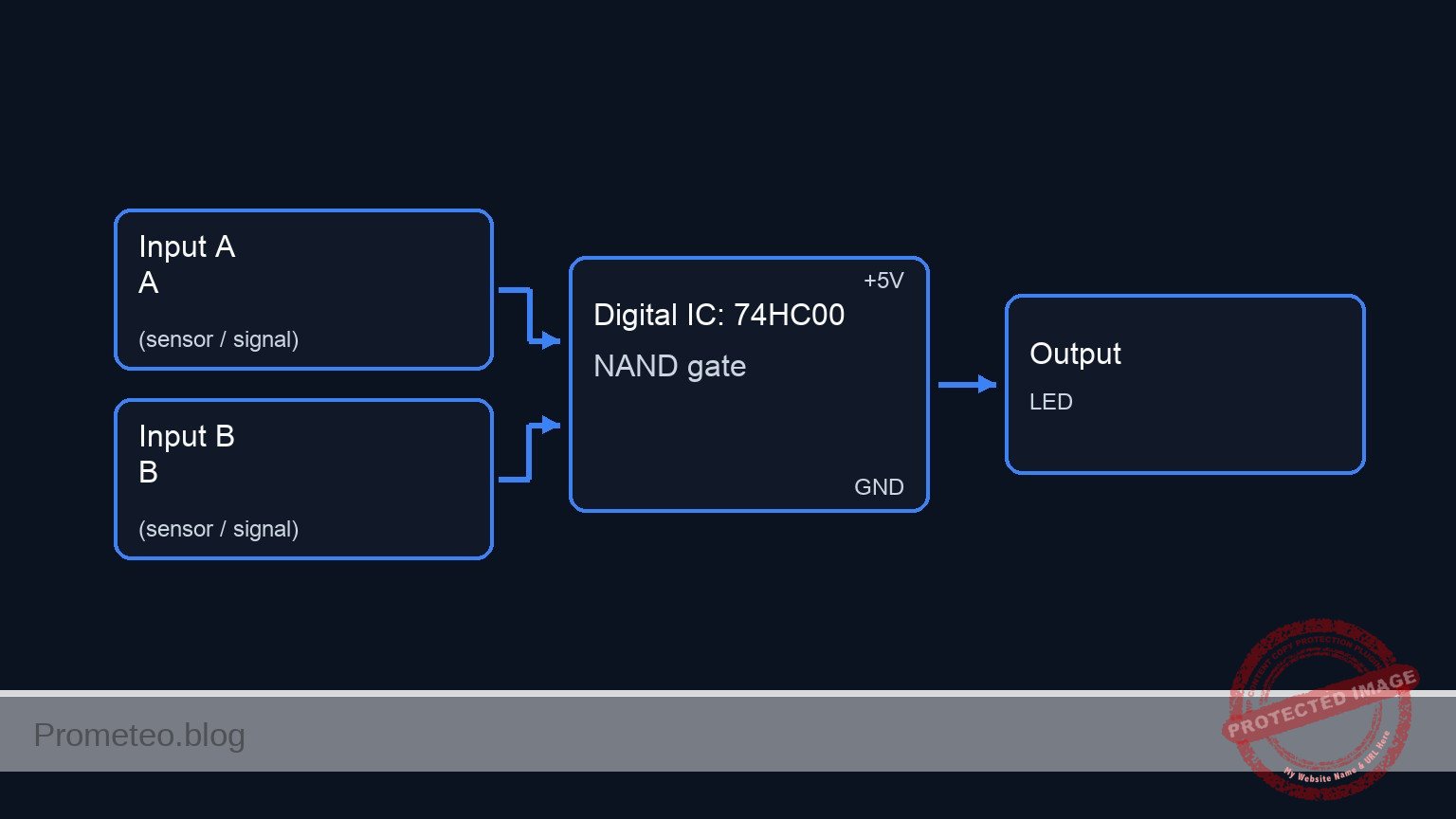
Conceptual block diagram

Conceptual block diagram — 74HC00 NAND gate
Quick read: inputs → main block → output (actuator or measurement). This summarizes the ASCII schematic below.

Schematic

Title: Practical case: Window sensor security alarm

(Input Stage: Sensors)                  (Processing Stage: Logic)             (Output Stage: Alarm)

[ VCC ]
   |
[ SW1: Window 1 ]
   |
   +--(SENS1)-------+-----------------> [ U1: Pin 1 (Input A) ]
                    |                                         |
                 [ R1: 10k ]                                  v
                    |                                 [ U1: NAND Gate ] --(ALARM_OUT)--> [ R3: 330 Ω ] --> [ D1: LED ] --> GND
                 [ GND ]                                      ^
                                                              |
[ VCC ]             |                                         |
   |                |                                         |
[ SW2: Window 2 ]   |                                         |
   |                |                                         |
   +--(SENS2)-------+-----------------> [ U1: Pin 2 (Input B) ]
                    |
                 [ R2: 10k ]
                    |
                 [ GND ]
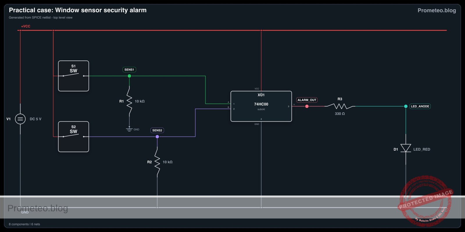
Electrical Schematic

Electrical diagram

Electrical diagram for case: Window sensor security alarm
Generated from the validated SPICE netlist for this case.

🔒 This electrical diagram is premium. With the monthly membership (7-day free trial) you can unlock the complete didactic material and the print-ready PDF pack.🔓 See premium access plans

Truth table

The 74HC00 implements the NAND function. In this security context, Logic 1 represents a «Closed Window» (Safe), and Logic 0 represents an «Open Window» (Breach).

Window 1 (SW1) Window 2 (SW2) Input A (Pin 1) Input B (Pin 2) Output Y (Pin 3) LED State Status
Closed Closed 1 (High) 1 (High) 0 (Low) OFF Secure
Open Closed 0 (Low) 1 (High) 1 (High) ON ALARM
Closed Open 1 (High) 0 (Low) 1 (High) ON ALARM
Open Open 0 (Low) 0 (Low) 1 (High) ON ALARM

Measurements and tests

Follow these steps to validate your alarm system:

  1. Initial Power-Up: Ensure both switches (SW1, SW2) are closed. Turn on the 5 V supply. The LED D1 should be OFF.
  2. Voltage Check (Secure): Use a multimeter to measure the voltage at node ALARM_OUT. It should be close to 0 V (< 0.2 V).
  3. Breach Test 1: Open SW1 while keeping SW2 closed. The LED should turn ON. Measure ALARM_OUT; it should read close to 5 V.
  4. Breach Test 2: Close SW1 and open SW2. The LED should turn ON.
  5. Total Breach: Open both switches. The LED should remain ON.

SPICE netlist and simulation

Reference SPICE Netlist (ngspice) — excerptFull SPICE netlist (ngspice)

* Practical case: Window sensor security alarm
.width out=256
* ngspice netlist

* --- Component Models ---
* Switch model for SW1 and SW2 (Sensors)
* Vt=2.5V: Switch closes when control voltage > 2.5V
* Ron=1m: Low resistance when closed
* Roff=100Meg: High resistance when open
.model SW_MOD SW(Vt=2.5 Ron=1m Roff=100Meg)

* LED model for D1
.model LED_RED D(IS=1e-22 RS=5 N=1.5 CJO=10p BV=5)

* --- Power Supply ---
* V1: 5 V DC power supply connected to VCC and 0 (GND)
V1 VCC 0 DC 5

* --- Window Sensor 1 ---
* Control source V_ACT1 simulates the physical action of opening/closing Window 1
* ... (truncated in public view) ...

Copy this content into a .cir file and run with ngspice.

🔒 Part of this section is premium. With the monthly membership (7-day free trial) you can access the full content (materials, wiring, detailed build, validation, troubleshooting, variants and checklist) and download the complete print-ready PDF pack.

* Practical case: Window sensor security alarm
.width out=256
* ngspice netlist

* --- Component Models ---
* Switch model for SW1 and SW2 (Sensors)
* Vt=2.5V: Switch closes when control voltage > 2.5V
* Ron=1m: Low resistance when closed
* Roff=100Meg: High resistance when open
.model SW_MOD SW(Vt=2.5 Ron=1m Roff=100Meg)

* LED model for D1
.model LED_RED D(IS=1e-22 RS=5 N=1.5 CJO=10p BV=5)

* --- Power Supply ---
* V1: 5 V DC power supply connected to VCC and 0 (GND)
V1 VCC 0 DC 5

* --- Window Sensor 1 ---
* Control source V_ACT1 simulates the physical action of opening/closing Window 1
* Logic: High (5V) = Window Closed, Low (0V) = Window Open
* Timing: Toggles every 100us (Period 200us)
V_ACT1 ACT1 0 PULSE(0 5 0 1u 1u 100u 200u)

* SW1: Connects VCC to SENS1 when window is closed
S1 VCC SENS1 ACT1 0 SW_MOD

* R1: Pull-down resistor for SENS1 (10k)
R1 SENS1 0 10k

* --- Window Sensor 2 ---
* Control source V_ACT2 simulates Window 2
* Timing: Toggles every 200us (Period 400us) to test all truth table combinations
V_ACT2 ACT2 0 PULSE(0 5 0 1u 1u 200u 400u)

* SW2: Connects VCC to SENS2 when window is closed
S2 VCC SENS2 ACT2 0 SW_MOD

* R2: Pull-down resistor for SENS2 (10k)
R2 SENS2 0 10k

* --- Logic IC: U1 (74HC00) ---
* Quad 2-input NAND gate. We instantiate one gate.
* Pin mapping according to wiring guide:
* Pin 1 (Input A) -> SENS1
* Pin 2 (Input B) -> SENS2
* Pin 3 (Output Y) -> ALARM_OUT
* Pin 7 -> GND (0), Pin 14 -> VCC
XU1 SENS1 SENS2 ALARM_OUT 0 VCC 74HC00_GATE

* Subcircuit for NAND Gate using robust continuous functions
.subckt 74HC00_GATE A B Y GND VCC
* Logic: Y = NAND(A, B) = NOT(A AND B)
* Implemented using sigmoid functions for convergence:
* 1 / (1 + exp(-k*(V-Vth))) acts as a smooth logical comparator.
* Vth = 2.5V, k = 20
B_NAND Y GND V = V(VCC) * (1 - ( (1/(1+exp(-20*(V(A)-2.5)))) * (1/(1+exp(-20*(V(B)-2.5)))) ))
.ends

* --- Alarm Output Indicator ---
* R3: Current limiting resistor (330 Ohm)
R3 ALARM_OUT LED_ANODE 330

* D1: Red LED connected to Ground
D1 LED_ANODE 0 LED_RED

* --- Simulation Commands ---
.op
* Transient analysis for 500us to capture all logic states
.tran 1u 500u

* Output configuration
* We print the Sensor inputs and the Alarm output
.print tran V(SENS1) V(SENS2) V(ALARM_OUT) V(LED_ANODE)

.end

Simulation Results (Transient Analysis)

Simulation Results (Transient Analysis)

Analysis: The simulation correctly implements the NAND logic truth table. When both sensors are High (5V, Closed), the Output is Low (~0V). If either or both sensors are Low (Open), the Output goes High (5V), activating the LED (approx 1.83V at anode).
Show raw data table (657 rows)
Index   time            v(sens1)        v(sens2)        v(alarm_out)    v(led_anode)
0	0.000000e+00	4.999500e-04	4.999500e-04	5.000000e+00	1.833072e+00
1	1.000000e-08	4.999500e-04	4.999500e-04	5.000000e+00	1.833072e+00
2	2.000000e-08	4.999500e-04	4.999500e-04	5.000000e+00	1.833072e+00
3	4.000000e-08	4.999500e-04	4.999500e-04	5.000000e+00	1.833072e+00
4	8.000000e-08	4.999500e-04	4.999500e-04	5.000000e+00	1.833072e+00
5	1.600000e-07	4.999500e-04	4.999500e-04	5.000000e+00	1.833072e+00
6	3.200000e-07	4.999500e-04	4.999500e-04	5.000000e+00	1.833072e+00
7	3.562500e-07	4.999500e-04	4.999500e-04	5.000000e+00	1.833072e+00
8	4.196875e-07	4.999500e-04	4.999500e-04	5.000000e+00	1.833072e+00
9	4.372461e-07	4.999500e-04	4.999500e-04	5.000000e+00	1.833072e+00
10	4.679736e-07	4.999500e-04	4.999500e-04	5.000000e+00	1.833072e+00
11	4.795524e-07	4.999500e-04	4.999500e-04	5.000000e+00	1.833072e+00
12	4.902290e-07	4.999500e-04	4.999500e-04	5.000000e+00	1.833072e+00
13	5.023412e-07	5.000000e+00	5.000000e+00	3.894872e-36	1.057689e+00
14	5.138120e-07	5.000000e+00	5.000000e+00	3.894872e-36	-7.61250e-02
15	5.160398e-07	5.000000e+00	5.000000e+00	3.894872e-36	-3.72798e-02
16	5.172425e-07	5.000000e+00	5.000000e+00	3.894872e-36	-2.57490e-02
17	5.188923e-07	5.000000e+00	5.000000e+00	3.894872e-36	-1.54585e-02
18	5.214063e-07	5.000000e+00	5.000000e+00	3.894872e-36	-6.97976e-03
19	5.238372e-07	5.000000e+00	5.000000e+00	3.894872e-36	-3.25627e-03
20	5.261078e-07	5.000000e+00	5.000000e+00	3.894872e-36	-1.60566e-03
21	5.281984e-07	5.000000e+00	5.000000e+00	3.894872e-36	-8.40881e-04
22	5.304310e-07	5.000000e+00	5.000000e+00	3.894872e-36	-4.20300e-04
23	5.328536e-07	5.000000e+00	5.000000e+00	3.894872e-36	-1.97001e-04
... (633 more rows) ...

Common mistakes and how to avoid them

  1. Floating Inputs: Forgetting R1 or R2 causes the inputs to «float» when switches are open, leading to erratic LED flickering. Solution: Always ensure inputs have a path to ground (via pull-down resistors) when the switch is open.
  2. LED Polarity: Connecting the LED backwards prevents it from lighting up even when the alarm is active. Solution: Ensure the longer leg (Anode) faces the resistor and IC output.
  3. Incorrect Switch Wiring: Placing the switch in parallel with the resistor instead of in series with the voltage source creates a short circuit. Solution: Follow the wiring guide: VCC -> Switch -> Node -> Resistor -> GND.

Troubleshooting

  • Symptom: LED is always ON, even when switches are closed.
    • Cause: One of the switches is not making contact, or an input wire is loose.
    • Fix: Check continuity across SW1 and SW2; ensure pin 1 and pin 2 actually receive 5 V.
  • Symptom: LED never turns ON.
    • Cause: LED is reversed, IC is not powered, or R3 is too high.
    • Fix: Check pin 14 for 5 V. Reverse the LED. Verify R3 is 330 Ω, not 330 kΩ.
  • Symptom: Logic works reversed (LED ON when safe, OFF when open).
    • Cause: You may be using an AND gate (74HC08) instead of NAND, or your switch/resistor logic is inverted (Pull-ups instead of Pull-downs).
    • Fix: Verify the chip number is 74HC00.

Possible improvements and extensions

  1. Audible Alarm: Connect the base of an NPN transistor to ALARM_OUT to drive a 5 V active buzzer, adding sound to the light.
  2. Latching Alarm: Use the remaining gates in the 74HC00 to build an SR Latch. This would keep the alarm sounding even if the burglar closes the window immediately after entering.

More Practical Cases on Prometeo.blog

Find this product and/or books on this topic on Amazon

Go to Amazon

As an Amazon Associate, I earn from qualifying purchases. If you buy through this link, you help keep this project running.

Quick Quiz

Question 1: What is the primary objective of the digital logic circuit described in the text?


Question 2: Under which condition will the alarm remain silent (LED OFF)?


Question 3: What happens if a wire connected to one of the sensors is cut?


Question 4: What logic level represents a closed window in this circuit design?


Question 5: According to the NAND truth table behavior described, when is the Output LOW?


Question 6: This project is an example of what kind of design principle?


Question 7: What is the voltage output when the alarm is triggered (LED ON)?


Question 8: Which of the following is a listed use case for this circuit?


Question 9: What is the state of the output when both switches (windows) are closed?


Question 10: Who is the target audience for this project?


Carlos Núñez Zorrilla
Electronics & Computer Engineer

Telecommunications Electronics Engineer and Computer Engineer (official degrees in Spain).
Follow me: