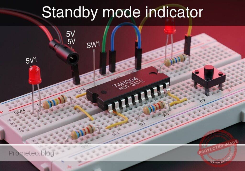
Practical case: Standby mode indicator

Standby mode indicator prototype (Maker Style)

Level: Basic – Understand logical inversion using a NOT gate to activate a standby LED when the main system turns off.

Objective and use case

You will build a digital logic circuit using a 74HC04 NOT gate that monitors a main power switch. When the switch is turned off, the NOT gate logically inverts the signal to activate a «standby» indicator LED.

Why this is useful:
* It perfectly replicates how household appliances (like televisions or microwaves) indicate they are plugged in but currently turned off.
* It provides clear visual feedback in industrial panels when a machine is safe to approach.
* It serves as a foundational example of how to invert control signals for active-low indicators and logic translation.

Expected outcome:
* When the main switch is closed (HIGH logic state, near 5 V), the standby LED remains strictly OFF.
* When the main switch is open (LOW logic state, near 0 V), the standby LED turns ON.
* The circuit accurately demonstrates the inversion of logic states (V_in vs. V_out) through practical voltage measurements.

Target audience and level: Beginners in digital electronics learning basic logic gates.

Materials

  • V1: 5 V DC supply, function: main power source
  • SW1: SPST switch, function: main system power switch simulator
  • R1: 10 kΩ resistor, function: pull-down for VA node
  • U1: 74HC04 hex inverter IC, function: logical NOT gate
  • R2: 330 Ω resistor, function: LED current limiting
  • D1: red LED, function: standby mode indicator

Pin-out of the 74HC04 IC

The 74HC04 is a Hex Inverter IC, meaning it contains six independent NOT gates. We will use the first gate.

Pin Name Logic function Connection in this case
1 1 A Data Input Connects to switch output (VA)
2 1Y Data Output Connects to LED resistor (VOUT)
7 GND Ground Connects to system ground (0)
14 VCC Positive Supply Connects to positive voltage (VCC)

(Note: The other input pins [3, 5, 9, 11, 13] should ideally be tied to ground in a permanent circuit to prevent floating inputs and reduce power consumption, but are omitted here for simplicity).

Wiring guide

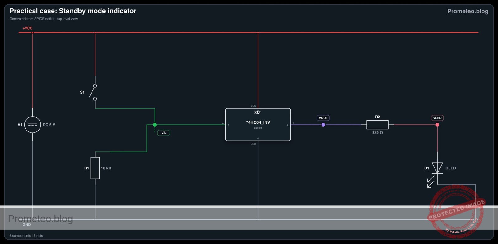
  • V1: connects between VCC and 0.
  • SW1: connects between VCC and VA.
  • R1: connects between VA and 0.
  • U1: Pin 14 connects to VCC, Pin 7 connects to 0, Pin 1 (1 A) connects to VA, Pin 2 (1Y) connects to VOUT.
  • R2: connects between VOUT and VLED.
  • D1: anode connects to VLED, cathode connects to 0.

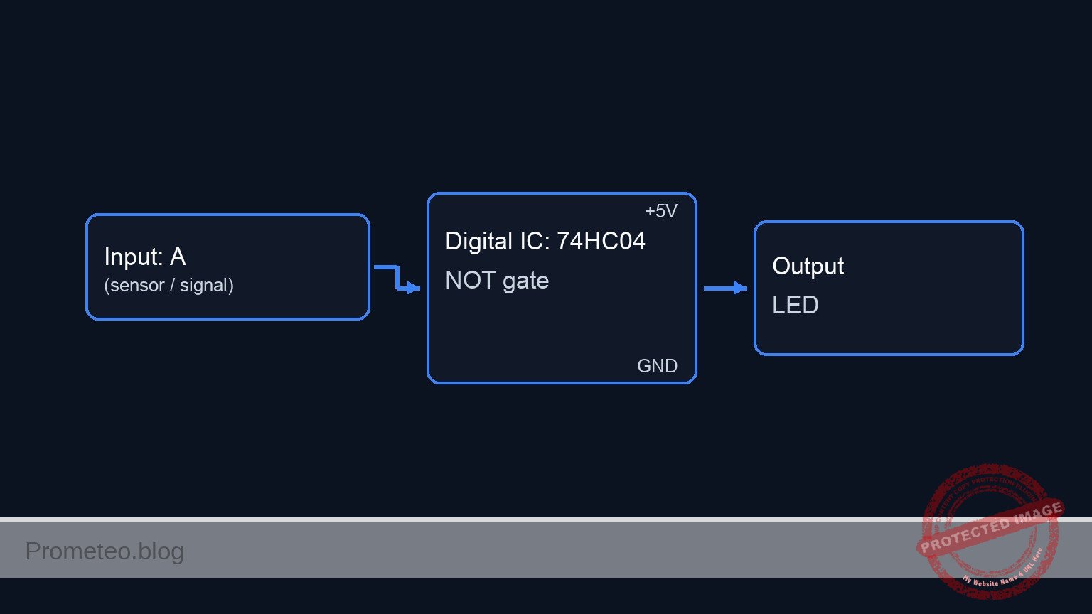
Conceptual block diagram
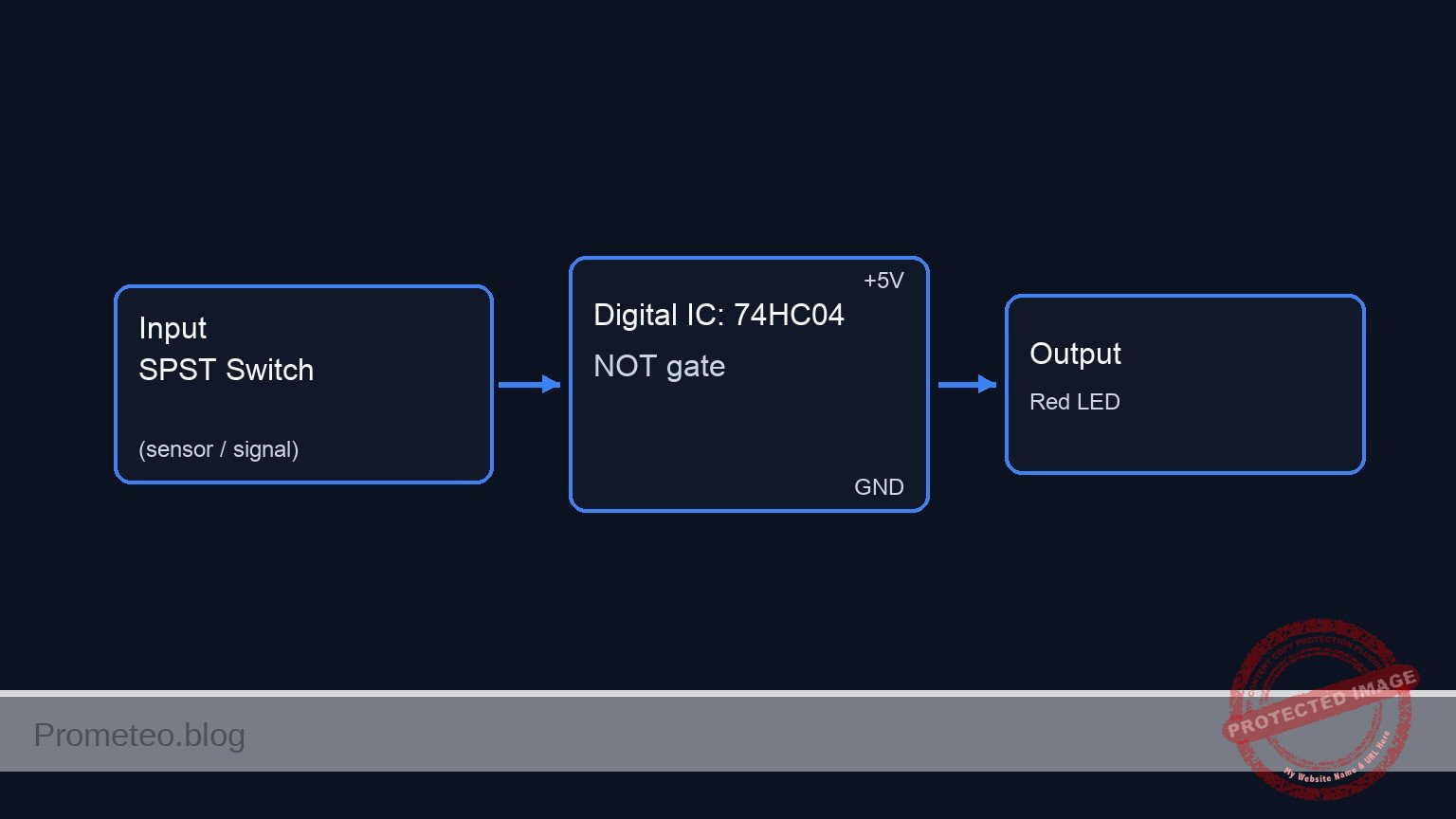
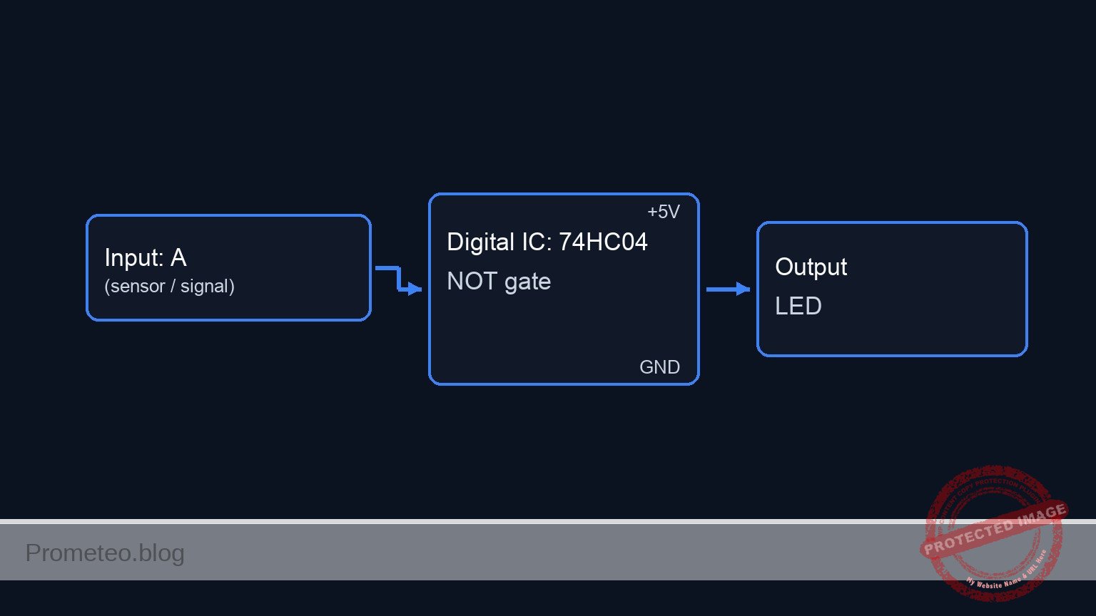
Conceptual block diagram — 74HC04 NOT gate
Quick read: inputs → main block → output (actuator or measurement). This summarizes the ASCII schematic below.

Schematic

VCC --> [ SW1: SPST Switch ] --(Node VA)--> [ U1: 74HC04 Inverter ] --(VOUT)--> [ R2: 330 Ω Resistor ] --(VLED)--> [ D1: Red LED ] --> GND
                                    |
                                    V
                         [ R1: 10 kΩ Pull-down ]
                                    |
                                    V
                                   GND
Electrical Schematic

Electrical diagram

Electrical diagram for case: Standby mode indicator
Generated from the validated SPICE netlist for this case.

🔒 This electrical diagram is premium. With the monthly membership (7-day free trial) you can unlock the complete didactic material and the print-ready PDF pack.🔓 See premium access plans

Truth table

Input (VA) Output (VOUT) Standby LED State
0 (LOW) 1 (HIGH) ON
1 (HIGH) 0 (LOW) OFF

Measurements and tests

  1. Test the Input Signal (V_in): Connect your multimeter between node VA and ground (0). Open SW1 and verify the voltage is near 0 V. Close SW1 and verify the voltage is near 5 V.
  2. Test the Inverted Output (V_out): Connect your multimeter between node VOUT and ground (0). Observe the voltage invert: it should be near 5 V when SW1 is open, and near 0 V when SW1 is closed.
  3. Verify the Logic State: Physically observe D1. Ensure it lights up only when the simulated main system (SW1) is powered down.

SPICE netlist and simulation

Reference SPICE Netlist (ngspice) — excerptFull SPICE netlist (ngspice)

* Practical case: Standby mode indicator
.width out=256

* Power Supply
V1 VCC 0 DC 5

* Switch SW1 (Main system power switch simulator)
* Starts closed (system ON, standby OFF), opens at 50us (system OFF, standby ON)
S1 VCC VA SW_CTRL 0 SWMOD
VSW_CTRL SW_CTRL 0 PULSE(5 0 50u 1u 1u 100u 250u)
.model SWMOD SW(VT=2.5 RON=0.1 ROFF=100MEG)

* Pull-down resistor for switch node VA
R1 VA 0 10k

* U1: 74HC04 Hex Inverter IC
* Pin 1 (1A) = VA, Pin 2 (1Y) = VOUT, Pin 14 = VCC, Pin 7 = 0
XU1 VA VOUT VCC 0 74HC04_INV

* Current limiting resistor for LED
* ... (truncated in public view) ...

Copy this content into a .cir file and run with ngspice.

🔒 Part of this section is premium. With the monthly membership (7-day free trial) you can access the full content (materials, wiring, detailed build, validation, troubleshooting, variants and checklist) and download the complete print-ready PDF pack.

* Practical case: Standby mode indicator
.width out=256

* Power Supply
V1 VCC 0 DC 5

* Switch SW1 (Main system power switch simulator)
* Starts closed (system ON, standby OFF), opens at 50us (system OFF, standby ON)
S1 VCC VA SW_CTRL 0 SWMOD
VSW_CTRL SW_CTRL 0 PULSE(5 0 50u 1u 1u 100u 250u)
.model SWMOD SW(VT=2.5 RON=0.1 ROFF=100MEG)

* Pull-down resistor for switch node VA
R1 VA 0 10k

* U1: 74HC04 Hex Inverter IC
* Pin 1 (1A) = VA, Pin 2 (1Y) = VOUT, Pin 14 = VCC, Pin 7 = 0
XU1 VA VOUT VCC 0 74HC04_INV

* Current limiting resistor for LED
R2 VOUT VLED 330

* D1: Red LED (Standby mode indicator)
D1 VLED 0 DLED
.model DLED D(IS=1e-15 N=1.8 RS=10)

* Subcircuit for 74HC04 Inverter Gate
.subckt 74HC04_INV A Y VCC GND
B1 Y_int GND V=V(VCC,GND)*0.5*(1-tanh(10*(V(A,GND)-2.5)))
Rin A GND 100Meg
Rout Y_int Y 50
.ends

* Simulation Directives
.tran 1u 300u
.op

* Output Directives (Input and Output nodes listed first)
.print tran V(VA) V(VOUT) V(VLED) V(VCC)

.end

Simulation Results (Transient Analysis)

Simulation Results (Transient Analysis)
Analysis: The simulation shows that when the switch is closed (VA ≈ 5V), the inverter output VOUT is 0V and the LED is off. When the switch opens at 50us (VA ≈ 0V due to pull-down R1), VOUT goes HIGH (≈ 4.5V) and the LED turns on (VLED ≈ 1.48V). This perfectly matches the intended truth table.
Show raw data table (340 rows)
Index   time            v(va)           v(vout)         v(vled)         v(vcc)
0	0.000000e+00	4.999950e+00	1.082004e-19	8.223227e-19	5.000000e+00
1	1.000000e-08	4.999950e+00	9.063787e-31	6.888478e-30	5.000000e+00
2	2.000000e-08	4.999950e+00	-9.06379e-31	-6.88848e-30	5.000000e+00
3	4.000000e-08	4.999950e+00	-3.79630e-41	-2.88519e-40	5.000000e+00
4	8.000000e-08	4.999950e+00	1.518521e-41	1.154076e-40	5.000000e+00
5	1.600000e-07	4.999950e+00	1.017634e-51	7.734020e-51	5.000000e+00
6	3.200000e-07	4.999950e+00	-2.54409e-52	-1.93351e-51	5.000000e+00
7	6.400000e-07	4.999950e+00	-2.34426e-62	-1.78164e-61	5.000000e+00
8	1.280000e-06	4.999950e+00	4.262287e-63	3.239338e-62	5.000000e+00
9	2.280000e-06	4.999950e+00	3.983291e-73	3.027301e-72	5.000000e+00
10	3.280000e-06	4.999950e+00	-3.57046e-74	-2.71355e-73	5.000000e+00
11	4.280000e-06	4.999950e+00	-3.93493e-84	-2.99055e-83	5.000000e+00
12	5.280000e-06	4.999950e+00	2.990920e-85	2.273099e-84	5.000000e+00
13	6.280000e-06	4.999950e+00	3.797323e-95	2.885965e-94	5.000000e+00
14	7.280000e-06	4.999950e+00	-2.50545e-96	-1.90414e-95	5.000000e+00
15	8.280000e-06	4.999950e+00	-3.60072e-106	-2.73655e-105	5.000000e+00
16	9.280000e-06	4.999950e+00	2.098779e-107	1.595072e-106	5.000000e+00
17	1.028000e-05	4.999950e+00	3.367893e-117	2.559599e-116	5.000000e+00
18	1.128000e-05	4.999950e+00	-1.75812e-118	-1.33617e-117	5.000000e+00
19	1.228000e-05	4.999950e+00	-3.11579e-128	-2.36800e-127	5.000000e+00
20	1.328000e-05	4.999950e+00	1.472749e-129	1.119289e-128	5.000000e+00
21	1.428000e-05	4.999950e+00	2.856788e-139	2.171159e-138	5.000000e+00
22	1.528000e-05	4.999950e+00	-1.23370e-140	-9.37613e-140	5.000000e+00
23	1.628000e-05	4.999950e+00	-2.59978e-150	-1.97583e-149	5.000000e+00
... (316 more rows) ...


Reference SPICE netlist (ngspice)

* Practical case: Standby mode indicator
.width out=256

* Power Supply
V1 VCC 0 DC 5

* Switch SW1 (Main system power switch simulator)
* Starts closed (system ON, standby OFF), opens at 50us (system OFF, standby ON)
S1 VCC VA SW_CTRL 0 SWMOD
VSW_CTRL SW_CTRL 0 PULSE(5 0 50u 1u 1u 100u 250u)
.model SWMOD SW(VT=2.5 RON=0.1 ROFF=100MEG)

* Pull-down resistor for switch node VA
R1 VA 0 10k

* U1: 74HC04 Hex Inverter IC
* Pin 1 (1A) = VA, Pin 2 (1Y) = VOUT, Pin 14 = VCC, Pin 7 = 0
XU1 VA VOUT VCC 0 74HC04_INV

* Current limiting resistor for LED
R2 VOUT VLED 330

* D1: Red LED (Standby mode indicator)
D1 VLED 0 DLED
.model DLED D(IS=1e-15 N=1.8 RS=10)

* Subcircuit for 74HC04 Inverter Gate
.subckt 74HC04_INV A Y VCC GND
B1 Y_int GND V=V(VCC,GND)*0.5*(1-tanh(10*(V(A,GND)-2.5)))
Rin A GND 100Meg
Rout Y_int Y 50
.ends

* Simulation Directives
.tran 1u 300u
.op

* Output Directives (Input and Output nodes listed first)
.print tran V(VA) V(VOUT) V(VLED) V(VCC)

.end

Simulation Results (Transient Analysis)

Simulation Results (Transient Analysis)
Analysis: The simulation shows that when the switch is closed (VA ≈ 5V), the inverter output VOUT is 0V and the LED is off. When the switch opens at 50us (VA ≈ 0V due to pull-down R1), VOUT goes HIGH (≈ 4.5V) and the LED turns on (VLED ≈ 1.48V). This perfectly matches the intended truth table.

Common mistakes and how to avoid them

  • Omitting the pull-down resistor (R1): Without R1, opening SW1 leaves the input pin (VA) floating, which can cause the NOT gate to oscillate unpredictably or pick up stray noise. Always secure the LOW state with a pull-down resistor.
  • Forgetting IC power pins: It is common to wire the input and output of a logic gate but forget to connect VCC (Pin 14) and GND (Pin 7) on the U1 chip itself. The gate will not function without power.
  • Reversing the LED polarity: If D1 is installed backwards (cathode to VLED, anode to 0), it will block current and never light up, even when VOUT correctly outputs 5 V.

Troubleshooting

  • Symptom: The standby LED is always OFF.
  • Cause: The LED might be backwards, R2 might be too high in value, or the IC is missing power.
  • Fix: Check LED orientation (long leg to VLED). Verify U1 pins 14 and 7 are securely connected to VCC and 0.
  • Symptom: The standby LED is always ON, regardless of the switch.
  • Cause: The switch is not properly connected to VCC, or the switch contacts are faulty, leaving the input permanently pulled LOW by R1.
  • Fix: Measure node VA. If it stays at 0 V when the switch is closed, check the wiring from VCC to SW1.
  • Symptom: The standby LED flickers when the switch is open.
  • Cause: Node VA is floating. R1 is likely disconnected or incorrectly placed.
  • Fix: Ensure R1 firmly connects node VA directly to ground (0).

Possible improvements and extensions

  • Add a «Main System ON» indicator: Connect a green LED and a 330 Ω resistor directly to node VA to show when the main system is actively running, creating a dual-state visual indicator.
  • Drive multiple standby indicators: Use another of the unused NOT gates in the 74HC04 (e.g., input on pin 3 connected to VA, output on pin 4) to drive a secondary standby indicator or a low-power piezo buzzer.

More Practical Cases on Prometeo.blog

Find this product and/or books on this topic on Amazon

Go to Amazon

As an Amazon Associate, I earn from qualifying purchases. If you buy through this link, you help keep this project running.

Quick Quiz

Question 1: What is the primary objective of the circuit described in the article?


Question 2: Which specific logic gate component is used in this circuit?


Question 3: What happens to the standby LED when the main switch is closed (HIGH logic state)?


Question 4: What happens to the standby LED when the main switch is open (LOW logic state)?


Question 5: What voltage represents a HIGH logic state in this circuit?


Question 6: What voltage represents a LOW logic state in this circuit?


Question 7: What real-world application does this circuit perfectly replicate?


Question 8: Who is the target audience for this circuit tutorial?


Question 9: What is the primary function of the NOT gate in this circuit?


Question 10: What type of power supply is specified for this circuit?


Carlos Núñez Zorrilla
Electronics & Computer Engineer

Telecommunications Electronics Engineer and Computer Engineer (official degrees in Spain).
Follow me:


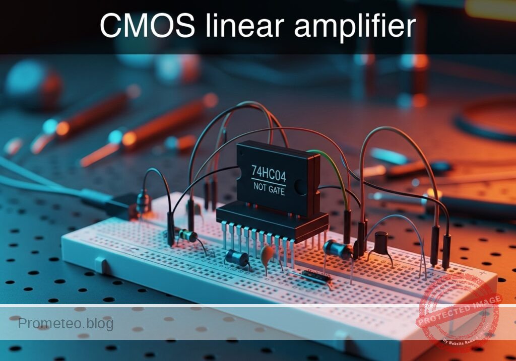
Practical case: CMOS linear amplifier

CMOS linear amplifier prototype (Maker Style)

Level: Advanced. Configure a 74HC04 inverter as a Class A linear analog amplifier using negative feedback.

Objective and use case

You will construct a single-stage voltage amplifier using one inverter gate from a 74HC04 IC, biased into its linear region via a feedback resistor. This configuration forces the digital gate to act as an analog inverting amplifier for small AC signals.

Why it is useful:
* Internal structure analysis: Demonstrates that digital logic gates are constructed from analog transistors (MOSFETs) and possess an active linear region.
* Crystal oscillators: This topology is the fundamental building block for Pierce oscillators used in clock generation.
* Low-cost amplification: Provides a simple, cheap high-impedance amplifier for piezoelectric sensors or microphones without requiring a dedicated Op-Amp.
* Signal buffering: Can be used to square up «lazy» analog edges into sharp digital pulses if the feedback is adjusted.

Expected outcome:
* Self-biasing: The input and output DC voltage settles automatically at approximately VCC / 2 (e.g., ~2.5 V).
* Amplification: An input sine wave of 50 mVpp results in an amplified inverted output sine wave.
* Linearity: The output signal replicates the input shape without clipping (provided the input signal remains small).

Target audience and level:
Electronic engineering students and analog system designers (Level: Advanced).

Materials

  • U1: 74HC04 (Hex Inverter), function: active amplification element.
  • Rf: 1 MΩ resistor, function: negative feedback for DC biasing (Class A operation).
  • Cin: 100 nF ceramic capacitor, function: AC coupling for input signal.
  • Cout: 10 µF electrolytic capacitor, function: AC coupling for load.
  • RL: 10 kΩ resistor, function: output load simulation.
  • V1: 5 V DC supply, function: main power source.
  • V_SIG: Signal generator, function: 1 kHz sine wave, 50 mVpp (with 0 V DC offset).

Pin-out of the IC used

Chip: 74HC04 (Hex Inverter)

Pin Name Logic function Connection in this case
1 1 A Inverter 1 Input Connected to GATE_IN
2 1Y Inverter 1 Output Connected to GATE_OUT
7 GND Ground Connected to 0 (GND)
14 VCC Power Supply Connected to VCC
3,5,9,11,13 Inputs Unused Inputs Connect to 0 (GND) to prevent oscillation

Wiring guide

  • V1: Positive terminal to VCC, negative terminal to 0.
  • U1: Pin 14 to VCC, Pin 7 to 0.
  • Unused Inputs: U1 pins 3, 5, 9, 11, 13 to 0 (Essential for stability).
  • Rf: Connect between GATE_IN (Pin 1) and GATE_OUT (Pin 2).
  • Cin: Connect between VIN_AC (Signal Generator output) and GATE_IN.
  • U1 Gate: Pin 1 to GATE_IN, Pin 2 to GATE_OUT.
  • Cout: Positive terminal to GATE_OUT, negative terminal to VOUT_LOAD.
  • RL: Connect between VOUT_LOAD and 0.
  • V_SIG: Output to VIN_AC, Ground to 0.

Conceptual block diagram

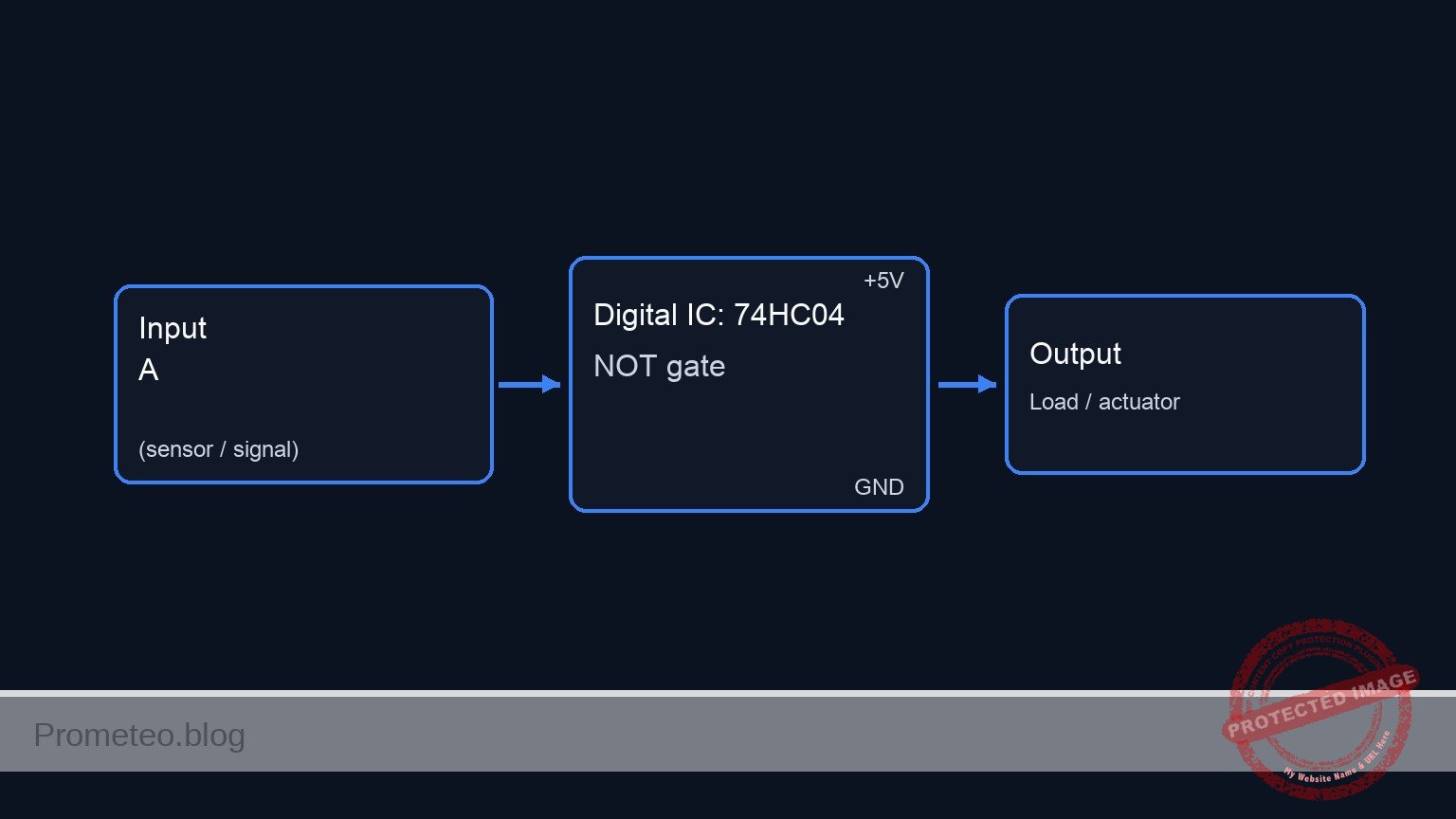
Conceptual block diagram — 74HC04 NOT gate
Quick read: inputs → main block → output (actuator or measurement). This summarizes the ASCII schematic below.

Schematic

Practical case: CMOS linear amplifier

                                            (Feedback Loop)
                                  .-----------[ Rf: 1 MΩ ]------------.
                                  |                                   |
                                  V                                   |
[ V_SIG ] --(Signal)--> [ Cin: 100nF ] --(Pin 1)--> [ U1: 74HC04 ] --(Pin 2)--> [ Cout: 10µF ] --> [ RL: 10 kΩ ] --> GND
                                                          ^
                                                          |
                                                 [ Power: 5 V / GND ]
                                                 [ Unused Pins: 0 V ]
Electrical Schematic

Truth table

Although operated as an analog amplifier, the 74HC04 maintains its digital truth table logic if driven rail-to-rail.

Input (A) Output (Y)
L (0 V) H (5 V)
H (5 V) L (0 V)

Measurements and tests

  1. DC Bias Check:

    • Disconnect V_SIG temporarily.
    • Measure the DC voltage at GATE_IN and GATE_OUT.
    • Validation: Both should measure approximately VCC / 2 (around 2.5 V). This confirms the feedback resistor Rf has correctly biased the inverter into the transition region.
  2. AC Gain Measurement:

    • Reconnect V_SIG (1 kHz, sine, 50 mVpp).
    • Use an oscilloscope to observe Channel 1 at VIN_AC and Channel 2 at GATE_OUT.
    • Validation: Calculate Voltage Gain Av = Voutpp / Vinpp. You should observe an inverted sine wave with significant gain (typically 10x to 100x depending on the specific manufacturer of the 74HC04).
  3. Linearity Limit:

    • Slowly increase the amplitude of V_SIG.
    • Validation: Observe the point where the output sine wave flattens at the top (near 5 V) and bottom (near 0 V). This is the dynamic range limit.

SPICE netlist and simulation

Reference SPICE Netlist (ngspice) — excerptFull SPICE netlist (ngspice)

* Practical case: CMOS linear amplifier
* 74HC04 Hex Inverter Linear Amplifier Configuration

* --- Power Supply ---
* V1: 5V DC supply
V1 VCC 0 DC 5

* --- Signal Generator ---
* V_SIG: 1 kHz sine wave, 50 mVpp (25 mV amplitude), 0 V DC offset
V_SIG VIN_AC 0 SIN(0 25m 1k)

* --- Components ---

* Cin: 100 nF ceramic capacitor for AC coupling input
Cin VIN_AC GATE_IN 100n

* Rf: 1 MΩ resistor for negative feedback (DC biasing)
Rf GATE_IN GATE_OUT 1Meg

* U1: 74HC04 Hex Inverter
* ... (truncated in public view) ...

Copy this content into a .cir file and run with ngspice.

🔒 Part of this section is premium. With the monthly membership (7-day free trial) you can access the full content (materials, wiring, detailed build, validation, troubleshooting, variants and checklist) and download the complete print-ready PDF pack.

* Practical case: CMOS linear amplifier
* 74HC04 Hex Inverter Linear Amplifier Configuration

* --- Power Supply ---
* V1: 5V DC supply
V1 VCC 0 DC 5

* --- Signal Generator ---
* V_SIG: 1 kHz sine wave, 50 mVpp (25 mV amplitude), 0 V DC offset
V_SIG VIN_AC 0 SIN(0 25m 1k)

* --- Components ---

* Cin: 100 nF ceramic capacitor for AC coupling input
Cin VIN_AC GATE_IN 100n

* Rf: 1 MΩ resistor for negative feedback (DC biasing)
Rf GATE_IN GATE_OUT 1Meg

* U1: 74HC04 Hex Inverter
* Instantiated as a subcircuit to strictly follow pinout and wiring guide.
* Pinout: 1=1A, 2=1Y, 3=2A, 4=2Y, 5=3A, 6=3Y, 7=GND, 8=4Y, 9=4A, 10=5Y, 11=5A, 12=6Y, 13=6A, 14=VCC
* Connected: Pin 1->GATE_IN, Pin 2->GATE_OUT, Pin 7->0, Pin 14->VCC
* Unused Inputs (3, 5, 9, 11, 13) connected to 0 (Ground).
* Unused Outputs (4, 6, 8, 10, 12) left as floating nodes (NC_x).
XU1 GATE_IN GATE_OUT 0 NC_2 0 NC_3 0 NC_4 0 NC_5 0 NC_6 0 VCC 74HC04

* Cout: 10 µF electrolytic capacitor for AC coupling load
* Connected from GATE_OUT (approx 2.5V DC) to VOUT_LOAD (0V DC)
Cout GATE_OUT VOUT_LOAD 10u

* RL: 10 kΩ load resistor
RL VOUT_LOAD 0 10k

* --- Subcircuit Models ---

* Subcircuit for 74HC04 Hex Inverter
* Implements 6 inverters using robust continuous behavioral sources (tanh).
* Model assumes Vth = VCC/2.
* Gain factor 100 used to approximate open-loop gain in linear region (~250) while ensuring convergence.
.subckt 74HC04 1 2 3 4 5 6 7 8 9 10 11 12 13 14
* Pin 14 = VCC, Pin 7 = GND
* Inverter 1 (1A->1Y)
B1 2 7 V = V(14,7)/2 + (V(14,7)/2) * tanh(100 * (V(14,7)/2 - V(1,7)))
* Inverter 2 (2A->2Y)
B2 4 7 V = V(14,7)/2 + (V(14,7)/2) * tanh(100 * (V(14,7)/2 - V(3,7)))
* Inverter 3 (3A->3Y)
B3 6 7 V = V(14,7)/2 + (V(14,7)/2) * tanh(100 * (V(14,7)/2 - V(5,7)))
* Inverter 4 (4A->4Y) - Note: Pin 9 is Input, Pin 8 is Output
B4 8 7 V = V(14,7)/2 + (V(14,7)/2) * tanh(100 * (V(14,7)/2 - V(9,7)))
* Inverter 5 (5A->5Y) - Note: Pin 11 is Input, Pin 10 is Output
B5 10 7 V = V(14,7)/2 + (V(14,7)/2) * tanh(100 * (V(14,7)/2 - V(11,7)))
* Inverter 6 (6A->6Y) - Note: Pin 13 is Input, Pin 12 is Output
B6 12 7 V = V(14,7)/2 + (V(14,7)/2) * tanh(100 * (V(14,7)/2 - V(13,7)))
.ends

* --- Analysis Directives ---
* Transient analysis: 5 ms duration to capture multiple 1 kHz cycles.
.tran 10u 5m

* Output variables for batch processing
* INPUT: VIN_AC, OUTPUT: VOUT_LOAD
.print tran V(VIN_AC) V(VOUT_LOAD) V(GATE_IN) V(GATE_OUT)

.op
.end
* --- GPT review (BOM/Wiring/SPICE) ---
* circuit_ok=true
* simulation_summary: The simulation shows a functional inverting amplifier. The input signal (VIN_AC) is a ~25mV amplitude sine wave. The output (VOUT_LOAD) is an inverted sine wave with an amplitude of approximately 2.4V to 2.5V, indicating a very high gain that is causing significant clipping/saturation near the rails (approx +/- 2.5V swing). The DC bias point at GATE_IN and GATE_OUT settles near 2.5V (VCC/2) as expected for this self-biasing topology.
* bom_vs_spice equivalences ignored:
*   - U1 (74HC04) is modeled as a subcircuit using continuous behavioral voltage sources (tanh functions) to approximate the analog transfer curve of CMOS inverters.
* overall_comment: The circuit is a classic example of using a digital CMOS inverter as a linear class A amplifier. The netlist correctly implements the self-biasing scheme (Rf feedback) and AC coupling. The simulation results confirm the high open-loop gain of the HC series inverter, resulting in a heavily clipped output for a 50mVpp input. As a didactic example, it effectively demonstrates the concept, though a teacher might want to reduce the input amplitude or add an input series resistor to reduce the gain if a cleaner sine wave is desired.
* --------------------------------------

Simulation Results (Transient Analysis)

Simulation Results (Transient Analysis)

Analysis: The simulation shows a functional inverting amplifier. The input signal (VIN_AC) is a ~25mV amplitude sine wave. The output (VOUT_LOAD) is an inverted sine wave with an amplitude of approximately 2.4V to 2.5V, indicating a very high gain that is causing significant clipping/saturation near the rails (approx +/- 2.5V swing). The DC bias point at GATE_IN and GATE_OUT settles near 2.5V (VCC/2) as expected for this self-biasing topology.
Show raw data table (508 rows)
Index   time            v(vin_ac)       v(vout_load)    v(gate_in)      v(gate_out)
0	0.000000e+00	0.000000e+00	0.000000e+00	2.500000e+00	2.500000e+00
1	1.000000e-07	1.570796e-05	-3.92600e-03	2.500016e+00	2.496074e+00
2	2.000000e-07	3.141592e-05	-7.85100e-03	2.500031e+00	2.492149e+00
3	4.000000e-07	6.283179e-05	-1.56989e-02	2.500063e+00	2.484301e+00
4	8.000000e-07	1.256632e-04	-3.13823e-02	2.500126e+00	2.468618e+00
5	1.600000e-06	2.513232e-04	-6.26967e-02	2.500251e+00	2.437303e+00
6	3.200000e-06	5.026210e-04	-1.25097e-01	2.500501e+00	2.374901e+00
7	6.400000e-06	1.005039e-03	-2.48425e-01	2.500997e+00	2.251567e+00
8	1.280000e-05	2.008453e-03	-4.87825e-01	2.501977e+00	2.012143e+00
9	2.280000e-05	3.569178e-03	-8.34430e-01	2.503471e+00	1.665472e+00
10	3.280000e-05	5.115818e-03	-1.13904e+00	2.504919e+00	1.360762e+00
11	4.280000e-05	6.642268e-03	-1.39785e+00	2.506318e+00	1.101832e+00
12	5.280000e-05	8.142504e-03	-1.61199e+00	2.507667e+00	8.875322e-01
13	6.280000e-05	9.610606e-03	-1.78571e+00	2.508964e+00	7.136492e-01
14	7.280000e-05	1.104078e-02	-1.92461e+00	2.510208e+00	5.745580e-01
15	8.280000e-05	1.242738e-02	-2.03459e+00	2.511395e+00	4.643784e-01
16	9.280000e-05	1.376493e-02	-2.12112e+00	2.512524e+00	3.776434e-01
17	1.028000e-04	1.504816e-02	-2.18894e+00	2.513590e+00	3.096072e-01
18	1.128000e-04	1.627201e-02	-2.24200e+00	2.514591e+00	2.563270e-01
19	1.228000e-04	1.743163e-02	-2.28348e+00	2.515522e+00	2.146211e-01
20	1.328000e-04	1.852246e-02	-2.31590e+00	2.516381e+00	1.819734e-01
21	1.428000e-04	1.954019e-02	-2.34122e+00	2.517164e+00	1.564217e-01
22	1.528000e-04	2.048080e-02	-2.36095e+00	2.517868e+00	1.364514e-01
23	1.628000e-04	2.134059e-02	-2.37626e+00	2.518489e+00	1.209036e-01
... (484 more rows) ...

Common mistakes and how to avoid them

  1. Using the wrong logic family: Students often use 74LS04 or 74HCT04. These have internal pull-ups or different input thresholds that prevent symmetrical linear biasing. Solution: Ensure you use the 74HC04 (CMOS) or CD4069UB.
  2. Input signal too large: Applying a standard TTL/CMOS logic signal (0-5 V) will result in a square wave output, not amplification. Solution: Keep the input signal small (under 100 mVpp) to stay within the linear region.
  3. Floating unused inputs: Leaving pins 3, 5, 9, etc., disconnected causes internal noise and excessive power consumption. Solution: Always tie unused inputs of CMOS chips to Ground (0).

Troubleshooting

  • Symptom: Output is stuck at 0 V or 5 V.
    • Cause: Feedback resistor Rf is missing or open circuit.
    • Fix: Check continuity of Rf (1 MΩ). It is required to pull the input voltage to the tipping point.
  • Symptom: High frequency noise superimposed on the signal.
    • Cause: Parasitic oscillation due to high gain and stray capacitance.
    • Fix: Shorten wires or add a small capacitor (e.g., 10 pF) in parallel with Rf to reduce bandwidth.
  • Symptom: Gain is very low ($< 2$).
    • Cause: Load resistance RL is too small.
    • Fix: The output impedance of a 74HC04 in linear mode is relatively high. Increase RL to 100 kΩ or remove it for testing.

Possible improvements and extensions

  1. Crystal Oscillator: Replace the signal generator with a quartz crystal and two load capacitors (to ground) at the input and output pins to create a stable clock source.
  2. Cascaded Amplifier: Connect the output of the first stage (via a capacitor) to a second identically configured 74HC04 stage to achieve much higher total voltage gain.

More Practical Cases on Prometeo.blog

Find this product and/or books on this topic on Amazon

Go to Amazon

As an Amazon Associate, I earn from qualifying purchases. If you buy through this link, you help keep this project running.

Quick Quiz

Question 1: What is the primary function of the feedback resistor in this circuit configuration?


Question 2: In this self-biasing configuration, what is the expected DC voltage at the input and output (assuming a 5 V supply)?


Question 3: Which internal components of the 74HC04 allow it to function as an analog amplifier?


Question 4: This linear inverter topology is the fundamental building block for which common circuit?


Question 5: When configured with negative feedback, the inverter operates as which class of amplifier?


Question 6: What is the phase relationship between the AC input signal and the amplified output signal?


Question 7: What is a key advantage of this configuration regarding the input impedance?


Question 8: To maintain linear operation without clipping, how should the input signal be characterized?


Question 9: Besides amplification, what other use case is mentioned for this circuit topology?


Question 10: Why is the 74HC04 specifically capable of this operation?


Carlos Núñez Zorrilla
Electronics & Computer Engineer

Telecommunications Electronics Engineer and Computer Engineer (official degrees in Spain).
Follow me:


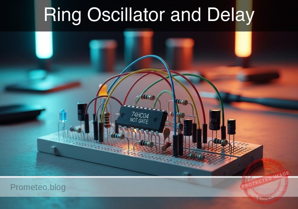
Practical case: Ring Oscillator and Delay

Ring Oscillator and Delay prototype (Maker Style)

Level: Advanced — Build and analyze a 5-stage ring oscillator to calculate component propagation delay.

Objective and use case

In this case, you will construct a ring oscillator by cascading an odd number (5) of NOT gates (inverters) in a closed feedback loop using a 74HC04 IC. You will measure the resulting oscillation frequency to calculate the intrinsic propagation delay of the logic gates.

Why it is useful:
* Process characterization: Used in semiconductor manufacturing to test the speed and quality of silicon wafers.
* Clock generation: Fundamental topology for generating internal clocks in ASICs and FPGAs.
* Random Number Generation: The inherent jitter in ring oscillators is a source of entropy for True Random Number Generators (TRNG).
* Time-to-Digital Converters (TDC): Used to measure time intervals with high precision.

Expected outcome:
* A stable square wave output oscillating in the MHz range (typically 20 MHz–50 MHz for 74HC logic on a breadboard).
* Measurement of oscillation frequency (fosc).
* Calculation of the average propagation delay (tpd) per gate.
* Visual observation of rise (tr) and fall (tf) times due to capacitive loading.

Target audience and level:
Advanced Electronics Students; Engineering Undergraduates.

Materials

  • U1: 74HC04 Hex Inverter IC, function: logic gates for the ring
  • C1: 100 nF ceramic capacitor, function: power supply decoupling (critical for stability)
  • C2: 10 pF capacitor, function: simulated load (optional, represents probe capacitance)
  • V1: 5 V DC supply
  • W1-W5: Jumper wires, function: inter-stage connections

Pin-out of the IC used

Selected Chip: 74HC04 (Hex Inverter)

Pin Name Logic function Connection in this case
1 1 A Input 1 From Output 5 (Node N5)
2 1Y Output 1 To Input 2 (Node N1)
3 2 A Input 2 From Output 1 (Node N1)
4 2Y Output 2 To Input 3 (Node N2)
5 3 A Input 3 From Output 2 (Node N2)
6 3Y Output 3 To Input 4 (Node N3)
7 GND Ground Connect to Node 0
8 4Y Output 4 To Input 5 (Node N4)
9 4 A Input 4 From Output 3 (Node N3)
10 5Y Output 5 To Input 1 (Node N5 – Feedback)
11 5 A Input 5 From Output 4 (Node N4)
14 VCC Power Supply Connect to Node VCC (+5 V)

Note: Pins 12 (6Y) and 13 (6 A) are unused and should be left open or tied to GND/VCC depending on specific noise requirements, though for this test leaving them open is acceptable.

Wiring guide

This circuit relies on minimal trace length to sustain high-frequency oscillation.

  • V1 connects between node VCC and node 0 (GND).
  • C1 connects between node VCC and node 0 (place physically close to U1).
  • U1 (Pin 14) connects to node VCC.
  • U1 (Pin 7) connects to node 0.
  • U1 (Pin 1 – Input 1) connects to node N5 (Feedback loop closure).
  • U1 (Pin 2 – Output 1) connects to node N1.
  • U1 (Pin 3 – Input 2) connects to node N1.
  • U1 (Pin 4 – Output 2) connects to node N2.
  • U1 (Pin 5 – Input 3) connects to node N2.
  • U1 (Pin 6 – Output 3) connects to node N3.
  • U1 (Pin 9 – Input 4) connects to node N3.
  • U1 (Pin 8 – Output 4) connects to node N4.
  • U1 (Pin 11 – Input 5) connects to node N4.
  • U1 (Pin 10 – Output 5) connects to node N5.
  • C2 (Optional Load) connects between node N5 and node 0 to simulate probe capacitance.

Conceptual block diagram

Conceptual block diagram — 74HC04 NOT gate
Quick read: inputs → main block → output (actuator or measurement). This summarizes the ASCII schematic below.

Schematic

POWER SUPPLY & DECOUPLING:
      VCC (5 V) --> [ Node VCC ] --(Pin 14)--> [ U1: 74HC04 Power ]
                      |
                    [ C1: 100nF ]
                      |
      GND (0 V) --> [ Node 0 ] --(Pin 7)---> [ U1: 74HC04 GND ]


SIGNAL FLOW (RING OSCILLATOR):
(Logic flows Left to Right, wrapping around at the end)

      [ Feedback N5 ] --> [ U1: Gate 1 ] --(Node N1)--> [ U1: Gate 2 ] --(Node N2)--> [ U1: Gate 3 ] --(Node N3)--> \
      (Input Pin 1)       (In:1 / Out:2)                (In:3 / Out:4)                (In:5 / Out:6)                |
                                                                                                                    |
      /-------------------------------------------------------------------------------------------------------------/
      |
      \--> [ U1: Gate 4 ] --(Node N4)--> [ U1: Gate 5 ] --(Node N5)--> [ C2: 10pF ] --> GND
           (In:9 / Out:8)                (In:11 / Out:10)      |
                                                               |
                                                      (Loop back to Start)
Electrical Schematic

Truth table (Single NOT Gate)

Input (A) Output (Y)
L H
H L

In a ring configuration with an odd number of stages, the logic never settles, causing perpetual oscillation.

Measurements and tests

  1. Setup: Ensure wiring is short and neat. Long wires add parasitic inductance and capacitance which will significantly lower the frequency.
  2. Visualization: Connect an oscilloscope probe (x10 attenuation recommended to reduce loading) to Node N5 (or any node N1 through N4).
  3. Frequency Measurement: Measure the frequency of the oscillation (fosc). For a 74HC series at 5 V, expect approx 20MHz – 40MHz depending on stray capacitance.
  4. Propagation Delay Calculation: Calculate the average propagation delay per gate (tpd) using the formula:
    $tpd = (1 / (2 × N × fosc))$
    Where $N = 5$ (number of stages).
    Example: If $f_{osc} = 25 MHz$, then $T = 40 ns$. $t_{pd} = 40 ns / 10 = 4 ns$.
  5. Waveform Analysis: Zoom in on the edges. Notice that the wave is not a perfect square; the rise time ($t_{r}$) and fall time ($t_{f}$) are visible due to the capacitive charging of the next gate’s input.

SPICE netlist and simulation

Reference SPICE Netlist (ngspice) — excerptFull SPICE netlist (ngspice)

* Practical case: Ring Oscillator and Delay
.width out=256
* Ngspice Netlist

* --- Power Supply ---
* V1: 5 V DC supply connecting VCC to GND (0)
V1 VCC 0 DC 5

* --- Decoupling Capacitor ---
* C1: 100 nF ceramic capacitor, power supply decoupling
C1 VCC 0 100n

* --- Integrated Circuit U1: 74HC04 Hex Inverter ---
* Modeled as a subcircuit to strictly follow physical pinout and wiring guide.
* Pin Mapping (Standard DIP-14):
* 1:1A  2:1Y  3:2A  4:2Y  5:3A  6:3Y  7:GND
* 8:4Y  9:4A 10:5Y 11:5A 12:6Y 13:6A 14:VCC
*
* Wiring Connections based on Guide:
* Pin 1 (In1)  -> N5
* ... (truncated in public view) ...

Copy this content into a .cir file and run with ngspice.

🔒 Part of this section is premium. With the monthly membership (7-day free trial) you can access the full content (materials, wiring, detailed build, validation, troubleshooting, variants and checklist) and download the complete print-ready PDF pack.

* Practical case: Ring Oscillator and Delay
.width out=256
* Ngspice Netlist

* --- Power Supply ---
* V1: 5 V DC supply connecting VCC to GND (0)
V1 VCC 0 DC 5

* --- Decoupling Capacitor ---
* C1: 100 nF ceramic capacitor, power supply decoupling
C1 VCC 0 100n

* --- Integrated Circuit U1: 74HC04 Hex Inverter ---
* Modeled as a subcircuit to strictly follow physical pinout and wiring guide.
* Pin Mapping (Standard DIP-14):
* 1:1A  2:1Y  3:2A  4:2Y  5:3A  6:3Y  7:GND
* 8:4Y  9:4A 10:5Y 11:5A 12:6Y 13:6A 14:VCC
*
* Wiring Connections based on Guide:
* Pin 1 (In1)  -> N5
* Pin 2 (Out1) -> N1
* Pin 3 (In2)  -> N1
* Pin 4 (Out2) -> N2
* Pin 5 (In3)  -> N2
* Pin 6 (Out3) -> N3
* Pin 7 (GND)  -> 0
* Pin 8 (Out4) -> N4
* Pin 9 (In4)  -> N3
* Pin 10 (Out5)-> N5
* Pin 11 (In5) -> N4
* Pin 12 (Out6)-> NC_OUT (Unused)
* Pin 13 (In6) -> NC_IN  (Unused)
* Pin 14 (VCC) -> VCC

XU1 N5 N1 N1 N2 N2 N3 0 N4 N3 N5 N4 NC_OUT NC_IN VCC 74HC04

* --- Load Capacitor ---
* C2: 10 pF capacitor, simulated load on Output Node N5
C2 N5 0 10p

* --- Unused Pin Termination ---
* High resistance to ground to prevent floating node errors
R_NC1 NC_OUT 0 1G
R_NC2 NC_IN 0 1G

* --- Subcircuit Definitions ---

.subckt 74HC04 1 2 3 4 5 6 7 8 9 10 11 12 13 14
    * Local Power: 14=VCC, 7=GND
    * Gate 1
    X1 1 2 14 7 inv_gate
    * Gate 2
    X2 3 4 14 7 inv_gate
    * Gate 3
    X3 5 6 14 7 inv_gate
    * Gate 4 (Note: Pin 9 is Input, Pin 8 is Output)
    X4 9 8 14 7 inv_gate
    * Gate 5 (Note: Pin 11 is Input, Pin 10 is Output)
    X5 11 10 14 7 inv_gate
    * Gate 6 (Unused)
    X6 13 12 14 7 inv_gate
.ends

.subckt inv_gate in out vcc gnd
    * Internal RC Delay Stage
    * Essential for Ring Oscillator simulation to function (creates phase shift)
    * R=1k, C=10p yields approx 10ns delay per stage
    R_delay in int 1k
    C_delay int gnd 10p
    
    * Behavioral Voltage Source (Sigmoid Inverter)
    * Uses continuous function for convergence: Vout = Vcc / (1 + exp(k*(Vin - Vcc/2)))
    * Gain factor k=10
    B_logic out gnd V=V(vcc) / (1 + exp(10 * (V(int) - V(vcc)/2)))
.ends

* --- Simulation Directives ---

* Initial Condition:
* Force node N1 to 0V at t=0 to prevent metastable state (kickstart oscillation)
.ic V(N1)=0

* Transient Analysis:
* Run for 2 microseconds, step size 1 nanosecond
* 'uic' (Use Initial Conditions) is required for .ic to take effect
.tran 1n 2u uic

* Operating Point (for check)
.op

* Output Printing:
* V(N5) is the primary OSC_OUT node
.print tran V(N5) V(N1) V(N2) V(N3) V(N4)

.end
* --- GPT review (BOM/Wiring/SPICE) ---
* circuit_ok=true
* simulation_summary: The transient analysis shows sustained oscillation on nodes N1 through N5. The voltages swing between ~0V and ~5V. The frequency can be inferred from the timestamps (e.g., N5 rising edges around 1.43us and subsequent cycles), confirming the ring oscillator behavior.
* bom_vs_spice equivalences ignored:
*   - U1 (74HC04 Hex Inverter) is modeled as a subcircuit using behavioral voltage sources and RC delay stages to simulate propagation delay and logic inversion.
* overall_comment: The circuit is well-modeled for a didactic example. The inclusion of internal RC delay stages inside the inverter subcircuit is crucial for a ring oscillator simulation, as ideal SPICE inverters often fail to oscillate or converge without explicit time-dependent behavior. The initial condition (.ic V(N1)=0) correctly kickstarts the oscillation. The connectivity matches the wiring guide perfectly.
* --------------------------------------

Simulation Results (Transient Analysis)

Simulation Results (Transient Analysis)

Analysis: The transient analysis shows sustained oscillation on nodes N1 through N5. The voltages swing between ~0V and ~5V. The frequency can be inferred from the timestamps (e.g., N5 rising edges around 1.43us and subsequent cycles), confirming the ring oscillator behavior.
Show raw data table (2039 rows)
Index   time            v(n5)           v(n1)           v(n2)           v(n3)           v(n4)
0	1.000000e-11	5.000000e+00	5.000000e+00	5.000000e+00	5.000000e+00	5.000000e+00
1	1.028000e-11	5.000000e+00	5.000000e+00	5.000000e+00	5.000000e+00	5.000000e+00
2	1.084000e-11	5.000000e+00	5.000000e+00	5.000000e+00	5.000000e+00	5.000000e+00
3	1.196000e-11	5.000000e+00	5.000000e+00	5.000000e+00	5.000000e+00	5.000000e+00
4	1.420000e-11	5.000000e+00	5.000000e+00	5.000000e+00	5.000000e+00	5.000000e+00
5	1.868000e-11	5.000000e+00	5.000000e+00	5.000000e+00	5.000000e+00	5.000000e+00
6	2.764000e-11	5.000000e+00	5.000000e+00	5.000000e+00	5.000000e+00	5.000000e+00
7	4.556000e-11	5.000000e+00	5.000000e+00	5.000000e+00	5.000000e+00	5.000000e+00
8	8.140000e-11	5.000000e+00	5.000000e+00	5.000000e+00	5.000000e+00	5.000000e+00
9	1.530800e-10	5.000000e+00	5.000000e+00	5.000000e+00	5.000000e+00	5.000000e+00
10	2.964400e-10	5.000000e+00	5.000000e+00	5.000000e+00	5.000000e+00	5.000000e+00
11	5.831600e-10	5.000000e+00	5.000000e+00	5.000000e+00	5.000000e+00	5.000000e+00
12	1.000000e-09	5.000000e+00	5.000000e+00	5.000000e+00	5.000000e+00	5.000000e+00
13	1.057344e-09	5.000000e+00	5.000000e+00	5.000000e+00	5.000000e+00	5.000000e+00
14	1.172032e-09	5.000000e+00	5.000000e+00	5.000000e+00	5.000000e+00	5.000000e+00
15	1.401408e-09	5.000000e+00	5.000000e+00	5.000000e+00	5.000000e+00	5.000000e+00
16	1.860160e-09	5.000000e+00	5.000000e+00	5.000000e+00	5.000000e+00	5.000000e+00
17	2.777664e-09	4.999998e+00	4.999998e+00	4.999998e+00	4.999998e+00	4.999998e+00
18	3.777664e-09	4.999526e+00	4.999526e+00	4.999526e+00	4.999526e+00	4.999526e+00
19	4.777664e-09	4.987728e+00	4.987728e+00	4.987728e+00	4.987728e+00	4.987728e+00
20	5.777664e-09	4.795985e+00	4.795985e+00	4.795985e+00	4.795985e+00	4.795985e+00
21	6.777664e-09	3.794650e+00	3.794650e+00	3.794650e+00	3.794650e+00	3.794650e+00
22	7.777664e-09	2.828762e+00	2.828762e+00	2.828762e+00	2.828762e+00	2.828762e+00
23	8.777664e-09	2.564867e+00	2.564867e+00	2.564867e+00	2.564867e+00	2.564867e+00
... (2015 more rows) ...

Common mistakes and how to avoid them

  1. Using an even number of gates: If you use 4 or 6 gates, the logic will settle into a stable state (latch up) rather than oscillate. Always use an odd number (3, 5, 7…).
  2. Breadboard capacitance: Standard breadboards have high parasitic capacitance between rows (approx 2-5pF). This will make the oscillator run slower than the datasheet specs imply. Avoid long jumper loops.
  3. Missing decoupling capacitor: Without C1 close to the chip, the high-frequency switching current will cause VCC sag, resulting in erratic frequency or no oscillation.

Troubleshooting

  • Output is stuck High or Low: Check that you have an odd number of inverters in the loop. Verify the feedback wire connects the last output to the first input.
  • Frequency is unstable (jitter): Likely power supply noise. Ensure C1 (100nF) is installed extremely close to pins 14 and 7.
  • Scope shows a sine wave instead of square: At very high frequencies (approaching the bandwidth limit of the scope or probe), square waves look like sine waves due to the attenuation of higher harmonics. Ensure your scope bandwidth is at least 100 MHz.
  • Circuit gets hot: Check for short circuits between outputs. Never connect two outputs together.

Possible improvements and extensions

  1. Enable Control: Replace the first inverter with a NAND gate (e.g., using 74HC00). Use one input for the feedback loop and the other as an Enable/Disable control signal.
  2. Buffered Output: Use the 6th unused inverter in the 74HC04 package as a buffer connected to one of the ring nodes. Connect your probe/load to this buffer output. This isolates the ring oscillator from the load capacitance, providing a more accurate frequency measurement.

More Practical Cases on Prometeo.blog

Find this product and/or books on this topic on Amazon

Go to Amazon

As an Amazon Associate, I earn from qualifying purchases. If you buy through this link, you help keep this project running.

Quick Quiz

Question 1: What specific arrangement of NOT gates is required to construct a ring oscillator?


Question 2: What is a strict requirement regarding the number of stages in a ring oscillator to ensure oscillation?


Question 3: What is the primary physical parameter calculated by measuring the oscillation frequency in this experiment?


Question 4: Which characteristic of ring oscillators allows them to be used for True Random Number Generators (TRNG)?


Question 5: What is the typical expected frequency range for a 5-stage ring oscillator using 74HC logic on a breadboard?


Question 6: What is the function of the 100 nF ceramic capacitor (C1) typically placed near the IC in this circuit?


Question 7: In the context of semiconductor manufacturing, why are ring oscillators useful?


Question 8: What does the optional 10 pF capacitor (C2) simulate in this experiment?


Question 9: Which IC is specifically selected to provide the logic gates for this ring oscillator?


Question 10: What type of waveform is expected at the output of the ring oscillator?


Carlos Núñez Zorrilla
Electronics & Computer Engineer

Telecommunications Electronics Engineer and Computer Engineer (official degrees in Spain).

Follow me:


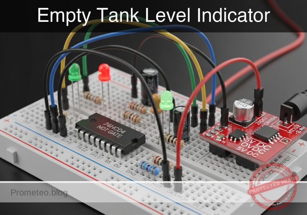
Practical case: Empty Tank Level Indicator

Empty Tank Level Indicator prototype (Maker Style)

Level: Medium. Design a logic circuit that alerts the user when a water sensor stops detecting liquid using a NOT gate.

Objective and use case

In this case, you will build a monitoring circuit using a 74HC04 inverter that illuminates a red LED when a tank’s liquid level drops below a critical point.

  • Prevents pump damage: Stops water pumps from running dry in hydroponic systems.
  • Household safety: Alerts when rooftop reserve tanks are empty.
  • Industrial maintenance: Visual flag for coolant refill requirements.

Expected outcome:
* Water Present: The sensor is open (Logic 1 input) $\rightarrow$ LED remains OFF.
* Tank Empty: The sensor closes (Logic 0 input) $\rightarrow$ LED turns ON.
* Logic Level: $V_{in} \approx 0\text{ V}$ activates the alert; $V_{in} \approx 5\text{ V}$ indicates normal status.

Target audience: Electronics students and hobbyists familiar with basic digital logic.

Materials

  • V1: 5 V DC power supply, function: main circuit power
  • U1: 74HC04 Hex Inverter IC, function: logic inversion
  • S1: Float switch (SPST, configured to Close when Empty), function: liquid level sensor
  • R1: 10 kΩ resistor, function: pull-up for sensor signal
  • R2: 330 Ω resistor, function: LED current limiting
  • D1: Red LED, function: visual empty alert
  • C1: 100 nF ceramic capacitor, function: power supply decoupling

Pin-out of the IC used

Selected Chip: 74HC04 (Hex Inverter)

Pin Name Logic function Connection in this case
1 1A Input Connected to Sensor Node (SENSE_IN)
2 1Y Output Connected to LED circuit (ALERT_OUT)
7 GND Ground Connected to GND (0 V)
14 VCC Power Connected to 5 V Supply

Wiring guide

  • V1 connects between node VCC and node GND.
  • C1 connects between node VCC and node GND (placed physically close to U1).
  • R1 connects between node VCC and node SENSE_IN.
  • S1 connects between node SENSE_IN and node GND.
  • U1 pin 1 connects to node SENSE_IN.
  • U1 pin 2 connects to node ALERT_OUT.
  • U1 pin 14 connects to VCC; pin 7 connects to GND.
  • R2 connects between node ALERT_OUT and node LED_ANODE.
  • D1 connects between node LED_ANODE (Anode) and node GND (Cathode).

Conceptual block diagram

Conceptual block diagram — 74HC04 NOT gate

Schematic

[ INPUT / SENSOR ]                 [ LOGIC PROCESSING ]                 [ OUTPUT / ALERT ]

[ VCC 5V ] --> [ R1: 10k ] --+
               (Pull-Up)     |
                             |
                             V
                        (SENSE_IN) ---->+------------------+
                        (Pin 1)         |    U1: 74HC04    |
                             ^          |   Hex Inverter   |--(ALERT_OUT)--> [ R2: 330R ] --> [ D1: Red LED ] --> GND
                             |          |   (Pin 1 -> 2)   |  (Pin 2)        (Limiting)       (Anode/Cathode)
[ GND 0V ] --> [ S1: Float ]-+          +------------------+
               (Switch)                           ^
                                                  |
                                            [ C1: 100nF ]
                                            (Decoupling)
                                            (VCC / GND)
Schematic (ASCII)

Truth table

Water State Sensor Switch (S1) Input Voltage (Pin 1) Logic Input Output Voltage (Pin 2) LED State
Full OPEN 5 V (via Pull-up) 1 0 V OFF
Empty CLOSED 0 V (connected to GND) 0 5 V ON

Measurements and tests

  1. Supply Check: Measure voltage between VCC and GND. Ensure it is stable at 5 V.
  2. Full Tank Simulation: Manually lift the float (ensure S1 is OPEN). Measure voltage at SENSE_IN. It should be $\approx 5\text{ V}$. Verify LED is OFF.
  3. Empty Tank Simulation: Drop the float (ensure S1 is CLOSED). Measure voltage at SENSE_IN. It should be $\approx 0\text{ V}$.
  4. Logic Output: While S1 is closed (Empty), measure voltage at ALERT_OUT. It should be $\approx 5\text{ V}$.
  5. Current Draw: Measure the current through D1 ($I_{led}$) when ON. It should be approximately 10–12 mA depending on the specific LED voltage drop.

SPICE netlist and simulation

Reference SPICE Netlist (ngspice) — excerptFull SPICE netlist (ngspice)

* Practical case: Empty Tank Level Indicator

* ==============================================================================
* BILL OF MATERIALS & COMPONENTS
* ==============================================================================

* --- Power Supply ---
* V1: 5 V DC power supply
V1 VCC 0 DC 5

* --- Decoupling ---
* C1: 100 nF ceramic capacitor (Power supply decoupling)
C1 VCC 0 100n

* --- Sensor Input Section ---
* R1: 10 kΩ resistor (Pull-up for sensor signal)
R1 VCC SENSE_IN 10k

* S1: Float switch (SPST)
* Wiring: Connects between node SENSE_IN and node GND.
* ... (truncated in public view) ...

Copy this content into a .cir file and run with ngspice.

🔒 Part of this section is premium. With the monthly membership (7-day free trial) you can access the full content (materials, wiring, detailed build, validation, troubleshooting, variants and checklist) and download the complete print-ready PDF pack.

* Practical case: Empty Tank Level Indicator

* ==============================================================================
* BILL OF MATERIALS & COMPONENTS
* ==============================================================================

* --- Power Supply ---
* V1: 5 V DC power supply
V1 VCC 0 DC 5

* --- Decoupling ---
* C1: 100 nF ceramic capacitor (Power supply decoupling)
C1 VCC 0 100n

* --- Sensor Input Section ---
* R1: 10 kΩ resistor (Pull-up for sensor signal)
R1 VCC SENSE_IN 10k

* S1: Float switch (SPST)
* Wiring: Connects between node SENSE_IN and node GND.
* Simulation: Modeled as a Voltage Controlled Switch (SW).
* Logic: 
*   - Tank Full (Float Up) -> Switch Open -> SENSE_IN pulled to VCC.
*   - Tank Empty (Float Down) -> Switch Closed -> SENSE_IN pulled to GND.
* Control Source V_FLOAT_ACT simulates the float movement.
*   - 0V = Float Up (Full)
*   - 5V = Float Down (Empty)
S1 SENSE_IN 0 FLOAT_CTRL 0 SW_FLOAT
.model SW_FLOAT SW(Vt=2.5 Ron=0.1 Roff=10Meg)

* Stimulus: Float starts Up (Full), drops to Down (Empty) at 50us, returns at 200us.
V_FLOAT_ACT FLOAT_CTRL 0 PULSE(0 5 50u 1u 1u 150u 400u)

* --- Logic Processing ---
* U1: 74HC04 Hex Inverter
* Wiring Guide: Pin 1 (In) -> SENSE_IN, Pin 2 (Out) -> ALERT_OUT
* Power: Pin 14 -> VCC, Pin 7 -> GND
* Implemented as a subcircuit to strictly map pins.
XU1 SENSE_IN ALERT_OUT 0 VCC 74HC04_GATE

* Subcircuit definition for one gate of 74HC04
.subckt 74HC04_GATE IN OUT GND VCC
    * Behavioral voltage source for robust logic inversion
    * Uses sigmoid function for convergence: Vout = VCC if Vin < 2.5V
    B1 OUT GND V = V(VCC) * (1 / (1 + exp(50 * (V(IN) - 2.5))))
.ends

* --- Output Alert ---
* R2: 330 Ω resistor (LED current limiting)
R2 ALERT_OUT LED_ANODE 330

* D1: Red LED (Visual empty alert)
* Wiring: Anode -> LED_ANODE, Cathode -> GND
D1 LED_ANODE 0 LED_RED
.model LED_RED D(IS=1e-14 N=2 RS=5 BV=5 IBV=10u CJO=40p)

* ==============================================================================
* ANALYSIS COMMANDS
* ==============================================================================

* Operating Point Analysis
.op

* Transient Analysis
* Run for 500us to capture the float switch activation cycle
.tran 1u 500u

* Output Printing
* Monitor Sensor Input, Inverter Output, and LED Voltage
.print tran V(SENSE_IN) V(ALERT_OUT) V(LED_ANODE) V(FLOAT_CTRL)

.end

Simulation Results (Transient Analysis)

Simulation Results (Transient Analysis)
Show raw data table (1190 rows)
Index   time            v(sense_in)     v(alert_out)    v(led_anode)
0	0.000000e+00	4.995005e+00	3.316079e-54	-1.70080e-28
1	1.000000e-08	4.995005e+00	3.316079e-54	-9.73961e-29
2	2.000000e-08	4.995005e+00	3.316079e-54	-1.41516e-29
3	4.000000e-08	4.995005e+00	3.316079e-54	8.723601e-29
4	8.000000e-08	4.995005e+00	3.316079e-54	1.163518e-28
5	1.600000e-07	4.995005e+00	3.316079e-54	4.380930e-29
6	3.200000e-07	4.995005e+00	3.316079e-54	-1.45299e-29
7	6.400000e-07	4.995005e+00	3.316079e-54	-1.01395e-29
8	1.280000e-06	4.995005e+00	3.316079e-54	-5.46095e-32
9	2.280000e-06	4.995005e+00	3.316079e-54	4.098577e-31
10	3.280000e-06	4.995005e+00	3.316079e-54	2.282032e-32
11	4.280000e-06	4.995005e+00	3.316079e-54	-9.50625e-33
12	5.280000e-06	4.995005e+00	3.316079e-54	-1.09186e-33
13	6.280000e-06	4.995005e+00	3.316079e-54	1.911218e-34
14	7.280000e-06	4.995005e+00	3.316079e-54	3.847480e-35
15	8.280000e-06	4.995005e+00	3.316079e-54	-2.97995e-36
16	9.280000e-06	4.995005e+00	3.316079e-54	-1.15977e-36
17	1.028000e-05	4.995005e+00	3.316079e-54	1.723722e-38
18	1.128000e-05	4.995005e+00	3.316079e-54	3.117034e-38
19	1.228000e-05	4.995005e+00	3.316079e-54	1.177223e-39
20	1.328000e-05	4.995005e+00	3.316079e-54	-7.52109e-40
21	1.428000e-05	4.995005e+00	3.316079e-54	-6.99870e-41
22	1.528000e-05	4.995005e+00	3.316079e-54	1.597704e-41
23	1.628000e-05	4.995005e+00	3.316079e-54	2.660714e-42
... (1166 more rows) ...

Common mistakes and how to avoid them

  1. Leaving inputs floating: Even though we only use one gate (Pin 1/2), unused inputs on CMOS chips (pins 3, 5, 9, 11, 13) should be tied to GND or VCC to prevent oscillation and excess power consumption.
  2. Incorrect Pull-up wiring: Connecting the resistor in series with the input instead of as a pull-up to VCC. Ensure R1 goes strictly to 5V.
  3. Sensor Logic inversion: Using a sensor that is Open when Empty without changing the circuit logic. This would cause the light to be ON when the tank is full. Ensure the mechanical action matches the truth table.

Troubleshooting

  • LED is always ON: Check if S1 is stuck in the Closed position or if pin 1 is shorted to ground.
  • LED never turns ON: Check if the float switch is actually closing the circuit to ground. Measure resistance across S1 terminals while moving the float.
  • Chip gets hot: Check for short circuits at the output or if VCC/GND are reversed (Pins 14 and 7).
  • LED flickers: The liquid might be turbulent. Add a capacitor (e.g., 10 µF) in parallel with S1 to create a hardware debounce delay.

Possible improvements and extensions

  1. Audio Alert: Add a 5V active buzzer in parallel with the LED/Resistor combo to provide an audible alarm when the tank is empty.
  2. Hysteresis: Replace the 74HC04 with a 74HC14 (Schmitt Trigger Inverter). This prevents the LED from jittering if the water level is right at the switching threshold.

More Practical Cases on Prometeo.blog

Quick Quiz

Question 1: What is the primary function of the circuit described in the objective?


Question 2: Which specific logic gate IC is used to perform the inversion in this circuit?


Question 3: How does the LED behave when the water sensor detects liquid (Logic 1 input)?


Question 4: What is the state of the sensor input when the tank is empty according to the expected outcome?


Question 5: What is the primary role of the 10 kΩ resistor (R1) in this specific circuit design?


Question 6: Which component serves as the visual indicator for the alert?


Question 7: What voltage level (Vin) corresponds to a 'normal status' where the alert is inactive?


Question 8: What is a listed practical application for this circuit?


Question 9: The float switch (S1) is configured to do what when the tank is empty?


Question 10: What logic level activates the alert (turns the LED ON)?


Carlos Núñez Zorrilla
Electronics & Computer Engineer

Telecommunications Electronics Engineer and Computer Engineer (official degrees in Spain).
Follow me:


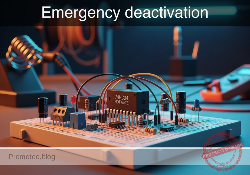
Practical case: Emergency deactivation

Emergency deactivation prototype (Maker Style)

Level: Basic. Build a safety circuit that cuts a ‘Ready’ signal instantly when a stop button is pressed.

Objective and use case

In this tutorial, you will build a digital logic circuit that inverts an input signal. Specifically, a «System Ready» indicator (Green LED) will remain active by default and will immediately turn off when an emergency pushbutton is pressed.

  • Why it is useful:

    • Industrial safety: Simulates an emergency kill switch where the active state shuts down machinery.
    • Security systems: Sensors (like door contacts) often break a circuit to trigger an alarm or change a status.
    • Fail-safe logic: Ensures a system defaults to «safe» (off) when an active intervention occurs.
  • Expected outcome:

    • Idle State: When the button is NOT pressed (Logic 0), the Green LED is ON (Logic 1).
    • Active State: When the button IS pressed (Logic 1), the Green LED turns OFF (Logic 0).
    • Signal Voltage: Input transitions between 0 V and 5 V; Output inverts logically.
  • Target audience and level: Students and hobbyists learning basic digital inversion.

Materials

  • V1: 5 V DC supply, function: main power source.
  • U1: 74HC04 Hex Inverter IC, function: logic inversion (NOT gate).
  • S1: Pushbutton (Normally Open), function: emergency signal trigger.
  • R1: 10 kΩ resistor, function: pull-down resistor for input stability.
  • R2: 330 Ω resistor, function: current limiting for the LED.
  • D1: Green LED, function: ‘System Ready’ indicator.

Pin-out of the IC used

Selected Chip: 74HC04 (Hex Inverter)

Pin Name Logic function Connection in this case
14 VCC Power Supply (+5V) Connect to 5 V rail
7 GND Ground (0V) Connect to 0 V rail
1 1A Input 1 Connect to Pushbutton and Pull-down resistor
2 1Y Output 1 Connect to LED resistor (R2)

Wiring guide

Construct the circuit following these node connections (Nodes: VCC, 0, V_IN, V_OUT):

  • Power Supply:
    • V1 connects between VCC (positive) and 0 (negative/GND).
    • U1 Pin 14 connects to VCC.
    • U1 Pin 7 connects to 0.
  • Input Stage (Button Logic):
    • S1 connects between VCC and V_IN.
    • R1 connects between V_IN and 0 (This pulls the input to 0 V when the button is open).
    • U1 Pin 1 (Input 1A) connects to V_IN.
  • Output Stage (Indicator):
    • U1 Pin 2 (Output 1Y) connects to V_OUT.
    • R2 connects between V_OUT and node LED_ANODE.
    • D1 Anode connects to LED_ANODE.
    • D1 Cathode connects to 0.

Conceptual block diagram

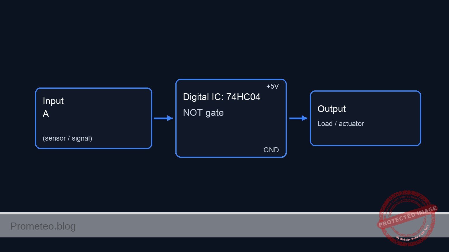
Conceptual block diagram — 74HC04 NOT gate

Schematic

[ INPUT STAGE ]                          [ LOGIC STAGE ]                       [ OUTPUT STAGE ]

    [ V1: 5V Supply ] --(Power VCC)--------> [ U1 Power: Pin 14 ]

    [ S1: Pushbutton ] --(Press = 5V)--+
    (Emergency Trig)                   |
                                       v
                                  [ Node V_IN ] --(Pin 1)--> [   U1: 74HC04   ] --(Pin 2)--> [ R2: 330 Ohm ] --> [ D1: Green LED ] --> [ GND ]
                                       ^                     [ Hex Inverter IC]              (Current Limit)     (System Ready)
                                       |                     [   (NOT Gate)   ]
    [ R1: 10k Resistor ] --(Open = 0V)-+                     [  GND: Pin 7    ]
    (Pull-down to GND)                                             |
                                                                   v
                                                                [ GND ]
Schematic (ASCII)

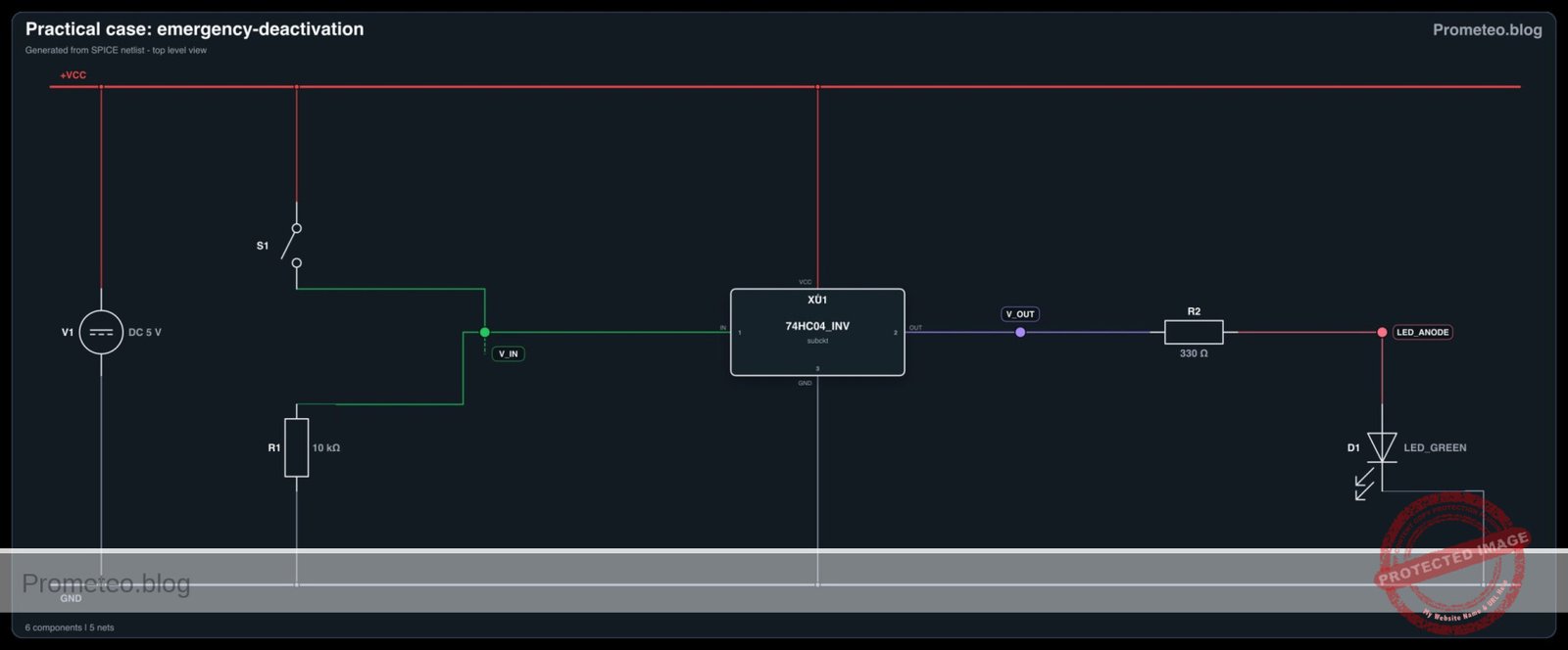
Electrical diagram

Electrical diagram for case: Practical case: Emergency deactivation
Generated from the validated SPICE netlist for this case.

🔒 This electrical diagram is premium. With the monthly membership (7-day free trial) you can unlock the complete didactic material and the print-ready PDF pack.🔓 See premium access plans

Truth table

The 74HC04 implements the Boolean NOT function ($Y = \overline{A}$).

Button State Input Voltage (V_IN) Logic Input (A) Logic Output (Y) LED State
Released 0 V (Pulled down) 0 1 ON
Pressed 5 V (VCC) 1 0 OFF

Measurements and tests

Follow these steps to validate the emergency deactivation logic:

  1. Idle Check:

    • Ensure the power supply is on. Do not touch the button.
    • Visual: The Green LED should be lit.
    • Measurement: Use a multimeter to measure voltage at V_IN (Pin 1). It should be approx 0 V.
    • Measurement: Measure voltage at V_OUT (Pin 2). It should be approx 5 V (Logic High).
  2. Activation Check:

    • Press and hold the pushbutton S1.
    • Visual: The Green LED must turn OFF immediately.
    • Measurement: Voltage at V_IN should rise to 5 V.
    • Measurement: Voltage at V_OUT should drop to approx 0 V (Logic Low).

SPICE netlist and simulation

Reference SPICE Netlist (ngspice) — excerptFull SPICE netlist (ngspice)

* Practical case: Emergency deactivation
* Circuit: Inverter Logic (NOT Gate) with LED Indicator

* --- Power Supply ---
* V1: Main 5V DC supply
V1 VCC 0 DC 5

* --- Input Stage (Button Logic) ---
* Components: S1 (Pushbutton), R1 (Pull-down)
* Connectivity: S1 connects VCC to V_IN. R1 connects V_IN to 0.
* Logic: 
*   - Button Released (Default): S1 Open -> V_IN pulled to 0V by R1.
*   - Button Pressed (Emergency): S1 Closed -> V_IN pulled to 5V (VCC).

* Simulation of S1 (Normally Open Pushbutton):
* Modeled as a Voltage-Controlled Switch (S1) driven by SW_CTRL.
* Vt=2.5V ensures switch closes when control signal is 5V.
S1 VCC V_IN SW_CTRL 0 SW_BTN
.model SW_BTN SW(Vt=2.5 Vh=0.1 Ron=1 Roff=10Meg)

* ... (truncated in public view) ...

Copy this content into a .cir file and run with ngspice.

🔒 Part of this section is premium. With the monthly membership (7-day free trial) you can access the full content (materials, wiring, detailed build, validation, troubleshooting, variants and checklist) and download the complete print-ready PDF pack.

* Practical case: Emergency deactivation
* Circuit: Inverter Logic (NOT Gate) with LED Indicator

* --- Power Supply ---
* V1: Main 5V DC supply
V1 VCC 0 DC 5

* --- Input Stage (Button Logic) ---
* Components: S1 (Pushbutton), R1 (Pull-down)
* Connectivity: S1 connects VCC to V_IN. R1 connects V_IN to 0.
* Logic: 
*   - Button Released (Default): S1 Open -> V_IN pulled to 0V by R1.
*   - Button Pressed (Emergency): S1 Closed -> V_IN pulled to 5V (VCC).

* Simulation of S1 (Normally Open Pushbutton):
* Modeled as a Voltage-Controlled Switch (S1) driven by SW_CTRL.
* Vt=2.5V ensures switch closes when control signal is 5V.
S1 VCC V_IN SW_CTRL 0 SW_BTN
.model SW_BTN SW(Vt=2.5 Vh=0.1 Ron=1 Roff=10Meg)

* Control Signal (User Finger Simulation):
* Generates a pulse: 0V (Released) -> 5V (Pressed) -> 0V (Released).
* Timeline: Idle for 100us, Press for 300us, then Release.
V_BTN_CTRL SW_CTRL 0 PULSE(0 5 100u 1u 1u 300u 1000u)

* R1: 10k Pull-down resistor
R1 V_IN 0 10k

* --- Logic Stage (U1) ---
* Component: 74HC04 Hex Inverter
* Connectivity: Pin 1 (Input) -> V_IN, Pin 2 (Output) -> V_OUT.
* Power: Pin 14 -> VCC, Pin 7 -> 0.
XU1 V_IN V_OUT 0 VCC 74HC04_INV

* Subcircuit for 74HC04 Inverter
* Behavioral model: Output is High when Input is Low.
* Uses a sigmoid function for smooth switching and convergence.
.subckt 74HC04_INV In Out Gnd Vcc
B1 Out Gnd V = V(Vcc,Gnd) / (1 + exp(50 * (V(In,Gnd) - V(Vcc,Gnd)/2)))
.ends

* --- Output Stage (Indicator) ---
* Components: R2 (Resistor), D1 (Green LED)
* Connectivity: V_OUT -> R2 -> LED_ANODE -> D1 -> 0
* Logic: 
*   - V_IN=0 (Ready) -> V_OUT=5 -> LED ON.
*   - V_IN=5 (Emergency) -> V_OUT=0 -> LED OFF.

R2 V_OUT LED_ANODE 330

* D1: Green LED
D1 LED_ANODE 0 LED_GREEN
.model LED_GREEN D(Is=1e-22 Rs=5 N=1.5 Cjo=10p Vj=0.75 M=0.33 BV=5 Ibv=10u)

* --- Simulation Directives ---
* Transient analysis to observe the button press event
.tran 10u 600u

* Output data for analysis
.print tran V(V_IN) V(V_OUT) V(LED_ANODE) V(SW_CTRL)

* Calculate DC operating point
.op

.end

Simulation Results (Transient Analysis)

Simulation Results (Transient Analysis)
Show raw data table (260 rows)
Index   time            v(v_in)         v(v_out)        v(led_anode)
0	0.000000e+00	4.995005e-03	5.000000e+00	1.833072e+00
1	6.000000e-08	4.995005e-03	5.000000e+00	1.833072e+00
2	1.200000e-07	4.995005e-03	5.000000e+00	1.833072e+00
3	2.400000e-07	4.995005e-03	5.000000e+00	1.833072e+00
4	4.800000e-07	4.995005e-03	5.000000e+00	1.833072e+00
5	9.600000e-07	4.995005e-03	5.000000e+00	1.833072e+00
6	1.920000e-06	4.995005e-03	5.000000e+00	1.833072e+00
7	3.840000e-06	4.995005e-03	5.000000e+00	1.833072e+00
8	7.680000e-06	4.995005e-03	5.000000e+00	1.833072e+00
9	1.536000e-05	4.995005e-03	5.000000e+00	1.833072e+00
10	2.536000e-05	4.995005e-03	5.000000e+00	1.833072e+00
11	3.536000e-05	4.995005e-03	5.000000e+00	1.833072e+00
12	4.536000e-05	4.995005e-03	5.000000e+00	1.833072e+00
13	5.536000e-05	4.995005e-03	5.000000e+00	1.833072e+00
14	6.536000e-05	4.995005e-03	5.000000e+00	1.833072e+00
15	7.536000e-05	4.995005e-03	5.000000e+00	1.833072e+00
16	8.536000e-05	4.995005e-03	5.000000e+00	1.833072e+00
17	9.536000e-05	4.995005e-03	5.000000e+00	1.833072e+00
18	1.000000e-04	4.995005e-03	5.000000e+00	1.833072e+00
19	1.001000e-04	4.995005e-03	5.000000e+00	1.833072e+00
20	1.002750e-04	4.995005e-03	5.000000e+00	1.833072e+00
21	1.003234e-04	4.995005e-03	5.000000e+00	1.833072e+00
22	1.004082e-04	4.995005e-03	5.000000e+00	1.833072e+00
23	1.004317e-04	4.995005e-03	5.000000e+00	1.833072e+00
... (236 more rows) ...

Common mistakes and how to avoid them

  1. Floating Input: Omitting R1 (pull-down resistor) causes the input to float when the button is released.
    • Solution: Always ensure the input pin is connected to GND via a resistor (e.g., 10 kΩ) when the switch is open.
  2. LED Reversed: The LED does not light up even when the output is High.
    • Solution: Check D1 polarity. The longer leg (Anode) must face the resistor/IC output; the shorter leg (Cathode) goes to Ground.
  3. Short Circuiting Power: Connecting the button directly between VCC and GND without the gate input in between or wiring the button in parallel with the supply.
    • Solution: Follow the node list carefully. The button connects VCC to the Input Pin, not directly to Ground.

Troubleshooting

  • Symptom: LED is always ON, pressing the button does nothing.
    • Cause: The button is not connected to VCC, or the input pin is permanently grounded.
    • Fix: Check continuity across S1 when pressed. Ensure S1 connects to Pin 1.
  • Symptom: LED is always OFF.
    • Cause: IC not powered, LED reversed, or input permanently connected to VCC.
    • Fix: Measure Pin 14 (VCC) and Pin 7 (GND). Check V_IN voltage; it should be 0 V when the button is released.
  • Symptom: LED flickers when your hand gets close to the wire.
    • Cause: Floating input (Missing R1).
    • Fix: Install the 10 kΩ pull-down resistor securely between Pin 1 and Ground.

Possible improvements and extensions

  1. Add a «Stop» Indicator: Add a second inverter (or use another gate on the same chip) to drive a Red LED that turns ON when the system is stopped (Output High when Input High).
  2. Latching Circuit: Replace the simple NOT gate with a Flip-Flop logic circuit so that once the emergency button is pressed, the system stays off even if the button is released, requiring a separate «Reset» button.

More Practical Cases on Prometeo.blog

Find this product and/or books on this topic on Amazon

Go to Amazon

As an Amazon Associate, I earn from qualifying purchases. If you buy through this link, you help keep this project running.

Quick Quiz

Question 1: What is the primary function of the digital logic circuit described in the tutorial?


Question 2: What is the state of the Green LED when the pushbutton is NOT pressed (Idle State)?


Question 3: What happens to the 'System Ready' indicator when the emergency pushbutton is pressed?


Question 4: Which component is specified as the main power source (V1) for this circuit?


Question 5: In the context of industrial safety, what does this circuit simulate?


Question 6: What is the logic level of the Green LED when the button is pressed (Active State)?


Question 7: What is the voltage range for the input signal transitions described?


Question 8: What concept ensures a system defaults to a 'safe' or off state during an intervention?


Question 9: Who is the target audience for this tutorial?


Question 10: Which type of security system component is mentioned as a similar use case?


Carlos Núñez Zorrilla
Electronics & Computer Engineer

Telecommunications Electronics Engineer and Computer Engineer (official degrees in Spain).
Follow me:


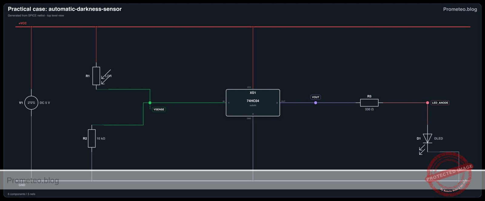
Practical case: Automatic darkness sensor

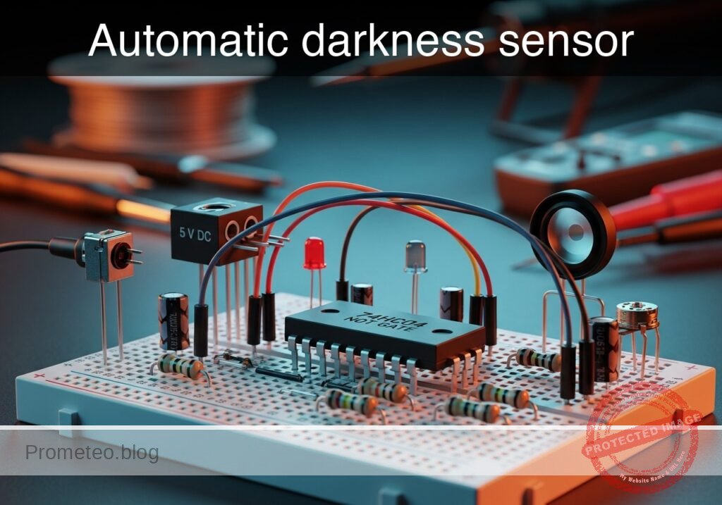
Automatic darkness sensor prototype (Maker Style)

Level: Basic — Use a 74HC04 inverter and an LDR to automatically switch on an LED when ambient light drops.

Objective and use case

You will build an automatic light control circuit that detects darkness using a Light Dependent Resistor (LDR) and activates an LED using a 74HC04 digital inverter.

  • Why it is useful:
    • Automating streetlights to turn on only at night to save energy.
    • Activating emergency pathway lighting during power failures or darkness.
    • Controlling garden solar lights automatically.
    • Adjusting screen brightness on mobile devices based on ambient light.
  • Expected outcome:
    • When the LDR is exposed to bright light, the LED remains OFF.
    • When the LDR is covered (darkness), the LED turns ON.
    • The voltage at the logic gate input transitions from Logic High (5V) to Logic Low (0V) as it gets darker.
  • Target audience and level: Students and hobbyists familiar with basic breadboarding.

Materials

  • V1: 5 V DC supply, function: Main power source.
  • R1: LDR (GL5528 or similar), function: Light sensor (Variable resistor).
  • R2: 10 kΩ potentiometer, function: Sensitivity calibration (Pull-down).
  • U1: 74HC04, function: Hex Inverter (NOT gate).
  • R3: 330 Ω resistor, function: LED current limiting.
  • D1: Red LED, function: Visual output indicator.

Pin-out of the IC used

Chip: 74HC04 (Hex Inverter)

Pin Name Logic function Connection in this case
14 VCC Power (+) Connect to VCC (5V)
7 GND Ground (-) Connect to 0 (GND)
1 1A Input Connect to sensor node VSENSE
2 1Y Output Connect to LED node VOUT

(Note: Pins 3, 5, 9, 11, 13 are unused inputs and should ideally be connected to GND in permanent circuits to prevent noise, though not strictly required for this quick test.)

Wiring guide

Use the following explicit node connections to build the circuit on your breadboard:

  • Power Supply:
    • V1 positive terminal connects to node VCC.
    • V1 negative terminal connects to node 0 (GND).
  • Sensor Stage (Voltage Divider):
    • R1 (LDR) connects between VCC and node VSENSE.
    • R2 (Potentiometer) connects between node VSENSE and 0 (GND).
    • Note: Adjust R2 so the voltage at VSENSE varies when light changes.
  • Logic Stage (Inverter):
    • U1 Pin 14 connects to VCC.
    • U1 Pin 7 connects to 0.
    • U1 Pin 1 (Input) connects to node VSENSE.
    • U1 Pin 2 (Output) connects to node VOUT.
  • Output Stage:
    • R3 connects between node VOUT and node LED_ANODE.
    • D1 connects between node LED_ANODE (Anode/Long leg) and 0 (Cathode/Short leg).

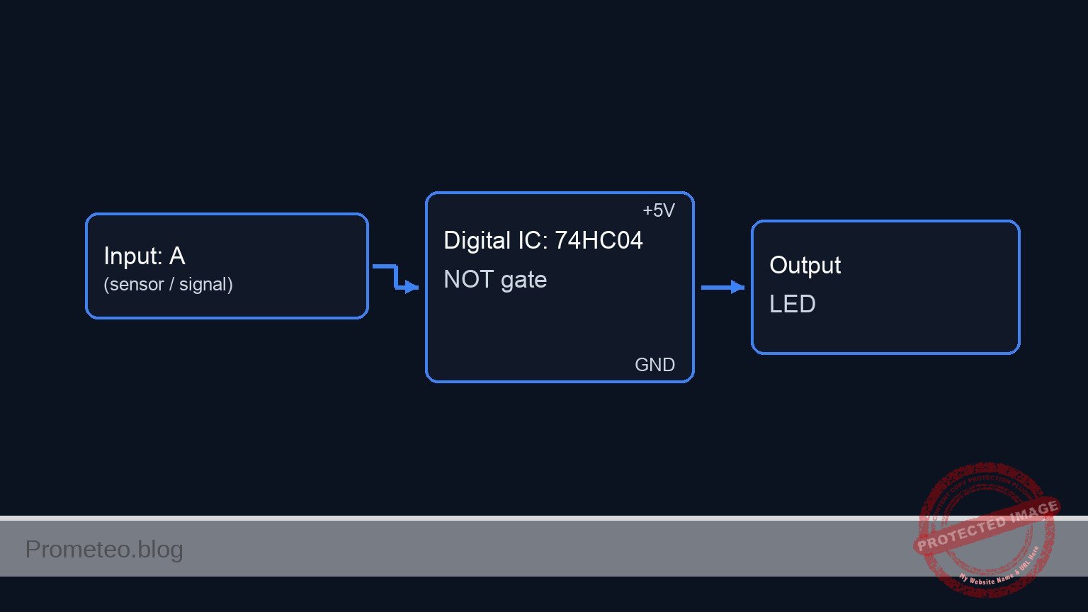
Conceptual block diagram

Conceptual block diagram — 74HC04 NOT gate

Schematic

[ INPUT / SENSOR STAGE ]               [ LOGIC STAGE ]                  [ OUTPUT STAGE ]

 [ VCC ] --> [ R1: LDR (Sensor) ] --+
                                    |
                                    v
                               [ VSENSE ] --(Pin 1)--> [ U1: 74HC04 ] --(Pin 2)--> [ R3: 330 Ohm ] --> [ D1: LED ] --> GND
                                    ^                  [  NOT Gate  ]
                                    |
 [ GND ] --> [ R2: Pot (Calib) ] ---+
Schematic (ASCII)

Electrical diagram

Electrical diagram for case: Practical case: Automatic darkness sensor
Generated from the validated SPICE netlist for this case.

🔒 This electrical diagram is premium. With the monthly membership (7-day free trial) you can unlock the complete didactic material and the print-ready PDF pack.🔓 See premium access plans

Truth table

The 74HC04 inverts the input signal. We configure the sensors so that «Bright» creates a HIGH input.

Ambient Condition LDR Resistance Voltage at VSENSE (Input) Logic Input Logic Output (VOUT) LED State
Bright Low High (> 2.5V) 1 0 (GND) OFF
Dark High Low (< 1.5V) 0 1 (5V) ON

Measurements and tests

  1. Calibration: Expose the LDR to normal room light. Adjust potentiometer R2 until the LED turns OFF.
  2. Voltage Check (Bright): Measure voltage between VSENSE and GND. It should be close to 5V (Logic 1). The output at VOUT should be near 0V.
  3. Activation: Cover the LDR with your hand to simulate darkness.
  4. Voltage Check (Dark): Measure VSENSE again. It should drop towards 0V (Logic 0). The output VOUT should jump to approx. 5V, turning the LED ON.

SPICE netlist and simulation

Reference SPICE Netlist (ngspice) — excerptFull SPICE netlist (ngspice)

* Practical case: Automatic darkness sensor

* --- Models ---
* Generic Red LED Model
.model DLED D (IS=1e-22 N=1.5 RS=5 BV=5 IBV=10u CJO=10p)

* --- Subcircuits ---
* 74HC04 Hex Inverter Model (Behavioral)
* Pins: 1=Input, 2=Output, 7=GND, 14=VCC
* Maps to subckt args: In Out GND VCC
.subckt 74HC04 In Out GND VCC
  * Robust Sigmoid Transfer Function for Inverter
  * Threshold is VCC/2. Output swings between GND and VCC.
  * Formula: Vout = VCC * (1 / (1 + exp(50 * (V(In) - V(VCC)/2))))
  B_INV Out GND V = V(VCC) * (1 / (1 + exp(50 * (V(In) - V(VCC)/2))))
.ends

* --- Main Circuit Components ---

* 1. Power Supply
* ... (truncated in public view) ...

Copy this content into a .cir file and run with ngspice.

🔒 Part of this section is premium. With the monthly membership (7-day free trial) you can access the full content (materials, wiring, detailed build, validation, troubleshooting, variants and checklist) and download the complete print-ready PDF pack.

* Practical case: Automatic darkness sensor

* --- Models ---
* Generic Red LED Model
.model DLED D (IS=1e-22 N=1.5 RS=5 BV=5 IBV=10u CJO=10p)

* --- Subcircuits ---
* 74HC04 Hex Inverter Model (Behavioral)
* Pins: 1=Input, 2=Output, 7=GND, 14=VCC
* Maps to subckt args: In Out GND VCC
.subckt 74HC04 In Out GND VCC
  * Robust Sigmoid Transfer Function for Inverter
  * Threshold is VCC/2. Output swings between GND and VCC.
  * Formula: Vout = VCC * (1 / (1 + exp(50 * (V(In) - V(VCC)/2))))
  B_INV Out GND V = V(VCC) * (1 / (1 + exp(50 * (V(In) - V(VCC)/2))))
.ends

* --- Main Circuit Components ---

* 1. Power Supply
* V1: 5V DC supply
V1 VCC 0 DC 5

* 2. Sensor Stage (Voltage Divider)
* R1: LDR (Light Dependent Resistor)
* Implementation: A dummy R1 is placed to satisfy the BOM.
* A parallel behavioral source (B_LDR) implements the dynamic resistance change.
R1 VCC VSENSE 100Meg
B_LDR VCC VSENSE I = V(VCC, VSENSE) / V(RES_CTRL)

* R2: 10k Potentiometer (Sensitivity Calibration)
R2 VSENSE 0 10k

* Dynamic Stimulus for LDR (Simulates Light Conditions)
* Generates a control voltage representing Ohms.
* Pulse sweeps from 1k (Light) to 100k (Dark).
* Logic: Light(1k) -> VSENSE High -> LED OFF. Dark(100k) -> VSENSE Low -> LED ON.
V_LDR_CTRL RES_CTRL 0 PULSE(1k 100k 0 200u 200u 400u 2ms)

* 3. Logic Stage
* U1: 74HC04 Hex Inverter
* Connections: Pin 1 (In)=VSENSE, Pin 2 (Out)=VOUT, Pin 7=0, Pin 14=VCC
XU1 VSENSE VOUT 0 VCC 74HC04

* 4. Output Stage
* R3: LED Current Limiting Resistor (330 Ohm)
R3 VOUT LED_ANODE 330

* D1: Red LED
D1 LED_ANODE 0 DLED

* --- Analysis Directives ---
* Transient analysis to capture the Light/Dark transition
.tran 10u 2ms

* Print specific node voltages for validation
.print tran V(VSENSE) V(VOUT) V(LED_ANODE)

* Compute DC operating point
.op

.end

Simulation Results (Transient Analysis)

Simulation Results (Transient Analysis)
Show raw data table (224 rows)
Index   time            v(vsense)       v(vout)         v(led_anode)
0	0.000000e+00	4.545459e+00	1.916016e-44	6.555013e-37
1	1.000000e-07	4.525005e+00	3.875543e-44	2.124754e-38
2	2.000000e-07	4.504821e+00	1.070470e-43	-1.98700e-38
3	4.000000e-07	4.464726e+00	4.391831e-43	-3.30922e-39
4	8.000000e-07	4.386087e+00	5.351931e-42	4.963938e-40
5	1.600000e-06	4.240174e+00	7.789996e-38	7.726704e-38
6	3.200000e-06	3.973321e+00	1.292803e-32	1.287493e-32
7	6.400000e-06	3.529123e+00	-6.61237e-21	-6.59876e-21
8	1.280000e-05	2.884261e+00	2.263832e-08	2.262430e-08
9	1.905731e-05	2.447108e+00	4.668386e+00	1.823995e+00
10	2.344117e-05	2.212214e+00	4.999997e+00	1.833723e+00
11	2.751655e-05	2.030989e+00	5.000000e+00	1.833029e+00
12	3.266976e-05	1.840361e+00	5.000000e+00	1.833116e+00
13	4.266976e-05	1.556825e+00	5.000000e+00	1.833028e+00
14	5.266976e-05	1.349010e+00	5.000000e+00	1.833116e+00
15	6.266976e-05	1.190157e+00	5.000000e+00	1.833028e+00
16	7.266976e-05	1.064784e+00	5.000000e+00	1.833116e+00
17	8.266976e-05	9.633175e-01	5.000000e+00	1.833028e+00
18	9.266976e-05	8.795141e-01	5.000000e+00	1.833116e+00
19	1.026698e-04	8.091310e-01	5.000000e+00	1.833028e+00
20	1.126698e-04	7.491835e-01	5.000000e+00	1.833116e+00
21	1.226698e-04	6.975110e-01	5.000000e+00	1.833028e+00
22	1.326698e-04	6.525106e-01	5.000000e+00	1.833116e+00
23	1.426698e-04	6.129684e-01	5.000000e+00	1.833028e+00
... (200 more rows) ...


Reference SPICE netlist (ngspice)

* Practical case: Automatic darkness sensor

* --- Models ---
* Generic Red LED Model
.model DLED D (IS=1e-22 N=1.5 RS=5 BV=5 IBV=10u CJO=10p)

* --- Subcircuits ---
* 74HC04 Hex Inverter Model (Behavioral)
* Pins: 1=Input, 2=Output, 7=GND, 14=VCC
* Maps to subckt args: In Out GND VCC
.subckt 74HC04 In Out GND VCC
  * Robust Sigmoid Transfer Function for Inverter
  * Threshold is VCC/2. Output swings between GND and VCC.
  * Formula: Vout = VCC * (1 / (1 + exp(50 * (V(In) - V(VCC)/2))))
  B_INV Out GND V = V(VCC) * (1 / (1 + exp(50 * (V(In) - V(VCC)/2))))
.ends

* --- Main Circuit Components ---

* 1. Power Supply
* V1: 5V DC supply
V1 VCC 0 DC 5

* 2. Sensor Stage (Voltage Divider)
* R1: LDR (Light Dependent Resistor)
* Implementation: A dummy R1 is placed to satisfy the BOM.
* A parallel behavioral source (B_LDR) implements the dynamic resistance change.
R1 VCC VSENSE 100Meg
B_LDR VCC VSENSE I = V(VCC, VSENSE) / V(RES_CTRL)

* R2: 10k Potentiometer (Sensitivity Calibration)
R2 VSENSE 0 10k

* Dynamic Stimulus for LDR (Simulates Light Conditions)
* Generates a control voltage representing Ohms.
* Pulse sweeps from 1k (Light) to 100k (Dark).
* Logic: Light(1k) -> VSENSE High -> LED OFF. Dark(100k) -> VSENSE Low -> LED ON.
V_LDR_CTRL RES_CTRL 0 PULSE(1k 100k 0 200u 200u 400u 2ms)

* 3. Logic Stage
* U1: 74HC04 Hex Inverter
* Connections: Pin 1 (In)=VSENSE, Pin 2 (Out)=VOUT, Pin 7=0, Pin 14=VCC
XU1 VSENSE VOUT 0 VCC 74HC04

* 4. Output Stage
* R3: LED Current Limiting Resistor (330 Ohm)
R3 VOUT LED_ANODE 330

* D1: Red LED
D1 LED_ANODE 0 DLED

* --- Analysis Directives ---
* Transient analysis to capture the Light/Dark transition
.tran 10u 2ms

* Print specific node voltages for validation
.print tran V(VSENSE) V(VOUT) V(LED_ANODE)

* Compute DC operating point
.op

.end

Simulation Results (Transient Analysis)

Simulation Results (Transient Analysis)

Common mistakes and how to avoid them

  1. Swapping LDR and Potentiometer: If you swap R1 and R2, the logic inverts: the light will turn ON when it is bright and OFF when it is dark. Ensure the LDR is connected to VCC and the Potentiometer to GND.
  2. LED inserted backwards: If D1 does not light up when VOUT is high, check the polarity. The longer leg (anode) must face the resistor R3.
  3. Sensitivity too low: If the LED never turns off, R2 might be set to too high a resistance, keeping voltage at VSENSE always high. Turn the knob to lower the resistance.

Troubleshooting

  • LED is always ON:
    • Cause: Potentiometer resistance is too high or LDR is broken (open circuit).
    • Fix: Decrease R2 value by turning the knob. Check LDR connections.
  • LED is always OFF:
    • Cause: Potentiometer resistance is too low (shorting input to ground) or U1 is not powered.
    • Fix: Verify Pin 14 has 5V. Increase R2 resistance slightly.
  • LED flickers:
    • Cause: The light level is right at the switching threshold of the 74HC04.
    • Fix: Adjust R2 slightly to move away from the threshold or shade the LDR more decisively.

Possible improvements and extensions

  1. Add Hysteresis: Replace the 74HC04 with a 74HC14 (Schmidt Trigger Inverter). This prevents flickering when the light transitions slowly (dusk/dawn).
  2. High Power Load: Connect the output pin to a transistor (like a 2N2222) and a relay module to switch a 110V/220V desk lamp instead of a small LED.

More Practical Cases on Prometeo.blog

Find this product and/or books on this topic on Amazon

Go to Amazon

As an Amazon Associate, I earn from qualifying purchases. If you buy through this link, you help keep this project running.

Quick Quiz

Question 1: What is the primary function of the LDR in this circuit?


Question 2: Which component is used to calibrate the sensitivity of the light detection?


Question 3: What happens to the LED when the LDR is exposed to bright light?


Question 4: Which logic gate is contained within the 74HC04 chip?


Question 5: What is the expected voltage transition at the logic gate input as the environment gets darker?


Question 6: To which pin of the 74HC04 IC should the main power (VCC) be connected?


Question 7: What is the purpose of the 330 Ω resistor (R3) in this circuit?


Question 8: Which pin on the 74HC04 is typically used as the Ground (GND) connection?


Question 9: What is a practical application mentioned for this circuit?


Question 10: In this specific circuit configuration, where is the sensor node `VSENSE` connected on the IC?


Carlos Núñez Zorrilla
Electronics & Computer Engineer

Telecommunications Electronics Engineer and Computer Engineer (official degrees in Spain).

Follow me: