Level: Advanced — Implement a 4-zone security system using cascaded OR logic to trigger a centralized alarm.
Objective and use case
In this project, you will build a centralized security monitoring system that supervises four distinct access points (windows or doors). The system uses magnetic reed switches and a 74HC32 Quad 2-input OR gate IC to consolidate multiple sensor signals into a single alarm trigger.
Why it is useful:
* Home Security: Monitors multiple entry points (front door, back door, garage, window) simultaneously.
* Server Rooms: Ensures all rack doors are closed; alerts if any single cabinet is breached.
* Industrial Safety: Prevents machine operation if any safety guard perimeter is open.
Expected outcome:
* Secure State: When all doors/windows are closed, the relay remains off (0 V at coil).
* Alarm State: If any single zone (or multiple zones) is breached, the relay activates.
* Voltage Levels: Logic Low (≈ 0 V) represents a secure zone; Logic High (≈ 5 V) represents a breach.
* Indication: A relay clicks and activates a connected load (simulated by a high-power LED or siren).
Target audience: Advanced electronics students and security system prototypers.
Materials
- V1: 5 V DC voltage source, function: Main power supply
- U1: 74HC32, function: Quad 2-input OR gate Logic IC
- S1: SPST Switch (Reed Switch), function: Zone 1 sensor (Normally Open, closed by magnet)
- S2: SPST Switch (Reed Switch), function: Zone 2 sensor
- S3: SPST Switch (Reed Switch), function: Zone 3 sensor
- S4: SPST Switch (Reed Switch), function: Zone 4 sensor
- R1: 10 kΩ resistor, function: Pull-up for Zone 1
- R2: 10 kΩ resistor, function: Pull-up for Zone 2
- R3: 10 kΩ resistor, function: Pull-up for Zone 3
- R4: 10 kΩ resistor, function: Pull-up for Zone 4
- R5: 1 kΩ resistor, function: Transistor base current limiting
- Q1: 2N2222 NPN Transistor, function: Relay driver
- D1: 1N4007 Diode, function: Flyback protection for relay coil
- RL1: 5 V Relay (SPDT), function: High-power switching interface
- C1: 100 nF capacitor, function: Decoupling for U1
Pin-out of the IC used
Chip: 74HC32 (Quad 2-Input OR Gate)
| Pin | Name | Logic Function | Connection in this case |
|---|---|---|---|
| 1 | 1A | Input OR Gate 1 | Connect to Node ZONE1 |
| 2 | 1B | Input OR Gate 1 | Connect to Node ZONE2 |
| 3 | 1Y | Output OR Gate 1 | Connect to Node INT_A (Input to Gate 3) |
| 4 | 2A | Input OR Gate 2 | Connect to Node ZONE3 |
| 5 | 2B | Input OR Gate 2 | Connect to Node ZONE4 |
| 6 | 2Y | Output OR Gate 2 | Connect to Node INT_B (Input to Gate 3) |
| 7 | GND | Ground | Connect to Node 0 |
| 9 | 3A | Input OR Gate 3 | Connect to Node INT_A |
| 10 | 3B | Input OR Gate 3 | Connect to Node INT_B |
| 8 | 3Y | Output OR Gate 3 | Connect to Node LOGIC_OUT |
| 14 | VCC | Power Supply | Connect to Node VCC |
Note: Pins 11, 12, and 13 (Gate 4) are unused and should be grounded if strictly following best CMOS practices, though often left floating in simple prototypes.
Wiring guide
This circuit uses «Active High» logic for alarms. The sensors are wired as Pull-ups. When a door is closed (magnet present), the switch closes to ground (Logic 0). When a door opens, the resistor pulls the line to VCC (Logic 1).
- Power Supply
- V1 positive terminal connects to node
VCC. - V1 negative terminal connects to node
0(GND). -
C1 connects between
VCCand0(near U1). -
Zone Sensors (Inputs)
- R1 connects between
VCCandZONE1. - S1 connects between
ZONE1and0. - R2 connects between
VCCandZONE2. - S2 connects between
ZONE2and0. - R3 connects between
VCCandZONE3. - S3 connects between
ZONE3and0. - R4 connects between
VCCandZONE4. -
S4 connects between
ZONE4and0. -
Logic Processing (Cascading)
- U1 Pin 1 (1A) connects to
ZONE1. - U1 Pin 2 (1B) connects to
ZONE2. - U1 Pin 3 (1Y) connects to
INT_A. - U1 Pin 4 (2A) connects to
ZONE3. - U1 Pin 5 (2B) connects to
ZONE4. - U1 Pin 6 (2Y) connects to
INT_B. - U1 Pin 9 (3A) connects to
INT_A. - U1 Pin 10 (3B) connects to
INT_B. -
U1 Pin 8 (3Y) connects to
LOGIC_OUT. -
Output Driver Stage
- R5 connects between
LOGIC_OUTand nodeBASE. - Q1 Base connects to
BASE. - Q1 Emitter connects to
0. - Q1 Collector connects to node
RELAY_COIL_NEG. - RL1 Coil positive connects to
VCC. - RL1 Coil negative connects to
RELAY_COIL_NEG. - D1 Anode connects to
RELAY_COIL_NEG. - D1 Cathode connects to
VCC(Parallel to coil, reverse biased).
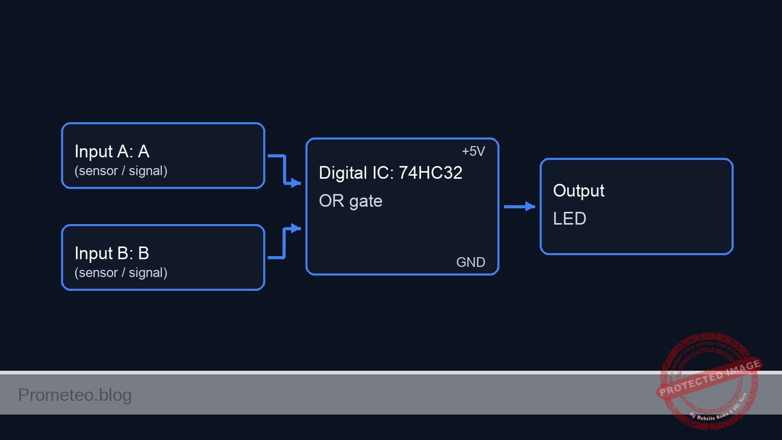
Conceptual block diagram

Schematic
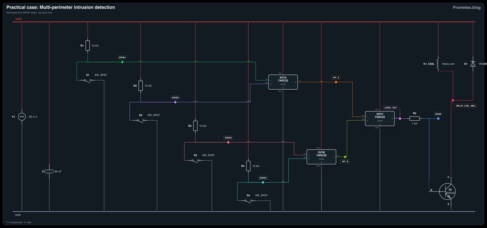
Title: Practical case: Multi-perimeter intrusion detection

      [ INPUT STAGE ]                  [ LOGIC STAGE (U1: 74HC32) ]                 [ OUTPUT STAGE ]

   (VCC)                                                                               (VCC)
     |                                                                                   |
   [ R1 ]                                                                            +---+---+
     +----(Zone 1)-------->+-------------+                                           |       |
     |                     |  OR GATE 1  |                                         [D1]    [RL1]
   [ S1 ]                  | (Pins 1,2)  |--(Int A)------>+                        (Diode) (Coil)
     |                     +-------------+                |                          |       |
   (GND)                   ^                              |                          +---+---+
                           |                              |                              |
   (VCC)                   |                              v                              |
     |                     |                       +-------------+                       |
   [ R2 ]                  |                       |  OR GATE 3  |                       |
     +----(Zone 2)---------+                       | (Pins 9,10) |                       |
     |                                             +-------------+                       |
   [ S2 ]                                                 |                              |
     |                                                    +----(Logic Out)--> [ R5 ] --> +
   (GND)                                                  ^                              |
                                                          |                         [ Q1 Base ]
   (VCC)                                                  |                              |
     |                                                    |                        [ Q1 (NPN) ]
   [ R3 ]                                                 |                              |
     +----(Zone 3)-------->+-------------+                |                         (Emitter)
     |                     |  OR GATE 2  |                |                              |
   [ S3 ]                  | (Pins 4,5)  |--(Int B)-------+                            (GND)
     |                     +-------------+
   (GND)                   ^
                           |
   (VCC)                   |
     |                     |
   [ R4 ]                  |
     +----(Zone 4)---------+
     |
   [ S4 ]
     |
   (GND)
Electrical diagram
Truth table
The logic is cascaded. Gates 1 and 2 handle the zones; Gate 3 combines their results.
Logic 0 = Secure (Door Closed). Logic 1 = Breach (Door Open).
| Zone 1 | Zone 2 | Zone 3 | Zone 4 | Int A (Z1+Z2) | Int B (Z3+Z4) | Final Output | System State |
|---|---|---|---|---|---|---|---|
| 0 | 0 | 0 | 0 | 0 | 0 | 0 | Secure |
| 1 | 0 | 0 | 0 | 1 | 0 | 1 | ALARM |
| 0 | 1 | 0 | 0 | 1 | 0 | 1 | ALARM |
| 0 | 0 | 1 | 0 | 0 | 1 | 1 | ALARM |
| 0 | 0 | 0 | 1 | 0 | 1 | 1 | ALARM |
| 1 | 1 | 1 | 1 | 1 | 1 | 1 | ALARM |
Note: Any combination containing at least one «1» results in a Final Output of «1».
Measurements and tests
- Static Logic Check:
- Ensure all switches are closed (magnets present). Measure voltage at
LOGIC_OUT. It should be < 0.1 V. - Open switch S1 only. Measure voltage at
ZONE1(should be ≈ 5 V) andLOGIC_OUT(should be ≈ 5 V). - Verify the Relay clicks ON.
- Ensure all switches are closed (magnets present). Measure voltage at
- Threshold Verification:
- With S1 open, measure the voltage at node
BASE(Q1 Base). It should be approx 0.7 V (Vbe of the transistor).
- With S1 open, measure the voltage at node
- Cascading Check:
- Close S1 (Secure). Open S3.
- Verify
INT_Ais Low (0 V) andINT_Bis High (5 V). - Verify
LOGIC_OUTremains High.
SPICE netlist and simulation
Reference SPICE Netlist (ngspice) — excerptFull SPICE netlist (ngspice)
* Multi-perimeter intrusion detection
* NGSPICE Netlist
* Created based on Bill of Materials and Wiring Guide

* =============================================================================
* COMPONENT MODELS
* =============================================================================

* NPN Transistor Model (2N2222)
.model 2N2222 NPN(Is=14.34f Xti=3 Eg=1.11 Vaf=74.03 Bf=255.9 Ne=1.307 Ise=14.34f
+ Ikf=.2847 Xtb=1.5 Br=6.092 Nc=2 Isc=0 Ikr=0 Rc=1 Cjc=7.306p Mjc=.3416 Vjc=.75
+ Fc=.5 Cje=22.01p Mje=.377 Vje=.75 Tr=46.91n Tf=411.1p Itf=.6 Vtf=1.7 Xtf=3 Rb=10)

* Diode Model (1N4007)
.model 1N4007 D(IS=7.027n RS=0.034 N=1.26 TT=4.32u CJO=4p)

* Voltage Controlled Switch Model (for Reed Switches)
* Vt=2.5V: Control > 2.5V is CLOSED (Low R), Control < 2.5V is OPEN (High R)
.model SW_REED SW(Vt=2.5 Ron=0.1 Roff=10Meg)

* ... (truncated in public view) ...
Copy this content into a .cir file and run with ngspice.
* Multi-perimeter intrusion detection
* NGSPICE Netlist
* Created based on Bill of Materials and Wiring Guide

* =============================================================================
* COMPONENT MODELS
* =============================================================================

* NPN Transistor Model (2N2222)
.model 2N2222 NPN(Is=14.34f Xti=3 Eg=1.11 Vaf=74.03 Bf=255.9 Ne=1.307 Ise=14.34f
+ Ikf=.2847 Xtb=1.5 Br=6.092 Nc=2 Isc=0 Ikr=0 Rc=1 Cjc=7.306p Mjc=.3416 Vjc=.75
+ Fc=.5 Cje=22.01p Mje=.377 Vje=.75 Tr=46.91n Tf=411.1p Itf=.6 Vtf=1.7 Xtf=3 Rb=10)

* Diode Model (1N4007)
.model 1N4007 D(IS=7.027n RS=0.034 N=1.26 TT=4.32u CJO=4p)

* Voltage Controlled Switch Model (for Reed Switches)
* Vt=2.5V: Control > 2.5V is CLOSED (Low R), Control < 2.5V is OPEN (High R)
.model SW_REED SW(Vt=2.5 Ron=0.1 Roff=10Meg)

* =============================================================================
* POWER SUPPLY
* =============================================================================
V1 VCC 0 DC 5

* =============================================================================
* SENSORS (ZONES 1-4)
* Logic: Door Closed (Magnet Present) -> Switch Closed to GND -> Zone Low (Safe)
*        Door Open (Magnet Removed) -> Switch Open -> Zone Pulled High (Alarm)
* Simulation: Control Voltage 5V = Door Closed. Control Voltage 0V = Door Open.
* =============================================================================

* --- ZONE 1 ---
R1 VCC ZONE1 10k
S1 ZONE1 0 CTRL1 0 SW_REED
* Stimulus: Door 1 opens briefly at 100us
V_S1_CTRL CTRL1 0 PULSE(5 0 100u 1u 1u 50u 10m)

* --- ZONE 2 ---
R2 VCC ZONE2 10k
S2 ZONE2 0 CTRL2 0 SW_REED
* Stimulus: Door 2 opens briefly at 300us
V_S2_CTRL CTRL2 0 PULSE(5 0 300u 1u 1u 50u 10m)

* --- ZONE 3 ---
R3 VCC ZONE3 10k
S3 ZONE3 0 CTRL3 0 SW_REED
* Stimulus: Door 3 opens briefly at 500us
V_S3_CTRL CTRL3 0 PULSE(5 0 500u 1u 1u 50u 10m)

* --- ZONE 4 ---
R4 VCC ZONE4 10k
S4 ZONE4 0 CTRL4 0 SW_REED
* Stimulus: Door 4 opens briefly at 700us
V_S4_CTRL CTRL4 0 PULSE(5 0 700u 1u 1u 50u 10m)

* =============================================================================
* LOGIC PROCESSING (U1: 74HC32 Quad OR Gate)
* =============================================================================

* Subcircuit for 74HC32 using robust behavioral sources (tanh)
* Pinout: 1=1A, 2=1B, 3=1Y, 4=2A, 5=2B, 6=2Y, 7=GND, 8=3Y, 9=3A, 10=3B, 11=4Y, 12=4A, 13=4B, 14=VCC
.subckt 74HC32 1A 1B 1Y 2A 2B 2Y GND 3Y 3A 3B 4Y 4A 4B VCC
    * Gate 1 (1A, 1B -> 1Y)
    B1 1Y GND V = 2.5 * (1 + tanh(10 * (V(1A) + V(1B) - 2.5)))
    * Gate 2 (2A, 2B -> 2Y)
    B2 2Y GND V = 2.5 * (1 + tanh(10 * (V(2A) + V(2B) - 2.5)))
    * Gate 3 (3A, 3B -> 3Y)
    B3 3Y GND V = 2.5 * (1 + tanh(10 * (V(3A) + V(3B) - 2.5)))
    * Gate 4 (4A, 4B -> 4Y) - Unused but modeled
    B4 4Y GND V = 2.5 * (1 + tanh(10 * (V(4A) + V(4B) - 2.5)))
.ends

* Decoupling Capacitor for U1
C1 VCC 0 100n

* Instantiate U1
* Connections based on Wiring Guide:
* 1->ZONE1, 2->ZONE2, 3->INT_A
* 4->ZONE3, 5->ZONE4, 6->INT_B
* 9->INT_A, 10->INT_B, 8->LOGIC_OUT
* 14->VCC, 7->0
* Unused inputs (12, 13) grounded to avoid floating nodes
XU1 ZONE1 ZONE2 INT_A ZONE3 ZONE4 INT_B 0 LOGIC_OUT INT_A INT_B NC_4Y 0 0 VCC 74HC32

* =============================================================================
* OUTPUT DRIVER STAGE
* =============================================================================

* Base Resistor
R5 LOGIC_OUT BASE 1k

* Driver Transistor Q1
Q1 RELAY_COIL_NEG BASE 0 2N2222

* Relay RL1 (Modeled as Coil Inductance + Resistance)
* Coil Positive -> VCC, Negative -> Collector
L_RL1 VCC RELAY_NODE_INT 100m
R_RL1 RELAY_NODE_INT RELAY_COIL_NEG 70

* Flyback Diode D1 (Parallel to coil, Reverse Biased)
* Anode -> Collector (Low side), Cathode -> VCC
D1 RELAY_COIL_NEG VCC 1N4007

* =============================================================================
* SIMULATION COMMANDS
* =============================================================================

.tran 10u 1000u

* Print required signals for validation
.print tran V(ZONE1) V(ZONE2) V(INT_A) V(INT_B) V(LOGIC_OUT) V(RELAY_COIL_NEG)

.op
.end
Simulation Results (Transient Analysis)

Show raw data table (742 rows)
Index   time            v(zone1)        v(zone2)        v(int_a)
0	0.000000e+00	4.999950e-05	4.999950e-05	0.000000e+00
1	1.000000e-07	4.999950e-05	4.999950e-05	0.000000e+00
2	2.000000e-07	4.999950e-05	4.999950e-05	0.000000e+00
3	4.000000e-07	4.999950e-05	4.999950e-05	0.000000e+00
4	8.000000e-07	4.999950e-05	4.999950e-05	0.000000e+00
5	1.600000e-06	4.999950e-05	4.999950e-05	0.000000e+00
6	3.200000e-06	4.999950e-05	4.999950e-05	0.000000e+00
7	6.400000e-06	4.999950e-05	4.999950e-05	0.000000e+00
8	1.280000e-05	4.999950e-05	4.999950e-05	0.000000e+00
9	2.280000e-05	4.999950e-05	4.999950e-05	0.000000e+00
10	3.280000e-05	4.999950e-05	4.999950e-05	0.000000e+00
11	4.280000e-05	4.999950e-05	4.999950e-05	0.000000e+00
12	5.280000e-05	4.999950e-05	4.999950e-05	0.000000e+00
13	6.280000e-05	4.999950e-05	4.999950e-05	0.000000e+00
14	7.280000e-05	4.999950e-05	4.999950e-05	0.000000e+00
15	8.280000e-05	4.999950e-05	4.999950e-05	0.000000e+00
16	9.280000e-05	4.999950e-05	4.999950e-05	0.000000e+00
17	1.000000e-04	4.999950e-05	4.999950e-05	0.000000e+00
18	1.001000e-04	4.999950e-05	4.999950e-05	0.000000e+00
19	1.002600e-04	4.999950e-05	4.999950e-05	0.000000e+00
20	1.003075e-04	4.999950e-05	4.999950e-05	0.000000e+00
21	1.003906e-04	4.999950e-05	4.999950e-05	0.000000e+00
22	1.004136e-04	4.999950e-05	4.999950e-05	0.000000e+00
23	1.004539e-04	4.999950e-05	4.999950e-05	0.000000e+00
... (718 more rows) ...
Common mistakes and how to avoid them
- Directly driving the relay with the IC:
- Error: Connecting the relay coil directly to the 74HC32 output pin. The chip cannot supply enough current (usually max 25mA, while relays need 70mA+).
- Solution: Always use a transistor (Q1) as a driver stage.
- Omitting the Flyback Diode (D1):
- Error: Leaving out D1 across the relay coil.
- Consequence: The high-voltage spike generated when the relay turns off can destroy the transistor Q1.
- Floating Inputs:
- Error: Forgetting the pull-up resistors (R1-R4) or the ground connection on the switches.
- Consequence: The CMOS inputs will float, causing erratic alarms or random switching due to electromagnetic noise.
Troubleshooting
- Symptom: Relay chatters (rapid clicking) or activates randomly.
- Cause: Noisy power supply or floating input pin.
- Fix: Check C1 is installed. Verify all unused inputs (if any) are tied to GND. Ensure pull-up resistors R1-R4 are securely connected.
- Symptom: Alarm does not trigger when Door 1 opens.
- Cause: Switch is stuck «Closed» or wiring error at U1 pin 1/2.
- Fix: Measure voltage at
ZONE1. If it stays 0 V when the door opens, the pull-up R1 is missing or shorted to ground.
- Symptom: Transistor Q1 gets hot or fails instantly.
- Cause: Missing base resistor R5.
- Fix: Ensure R5 (1 kΩ) is in series with the base to limit current.
Possible improvements and extensions
- Latching Alarm: Add a flip-flop or feedback loop (SCR logic) so that once the alarm triggers, it stays on even if the intruder closes the door again. A reset button would be required.
- Zone Indicators: Add an individual LED buffered from nodes
ZONE1throughZONE4. This allows the user to see exactly which specific window or door caused the alarm.
More Practical Cases on Prometeo.blog
Find this product and/or books on this topic on Amazon
As an Amazon Associate, I earn from qualifying purchases. If you buy through this link, you help keep this project running.
Quick Quiz

Telecommunications Electronics Engineer and Computer Engineer (official degrees in Spain).