Level: Medium. Implement a safety system that stops a conveyor belt if either the temperature sensor OR the jam sensor detects an anomaly.
Objective and use case
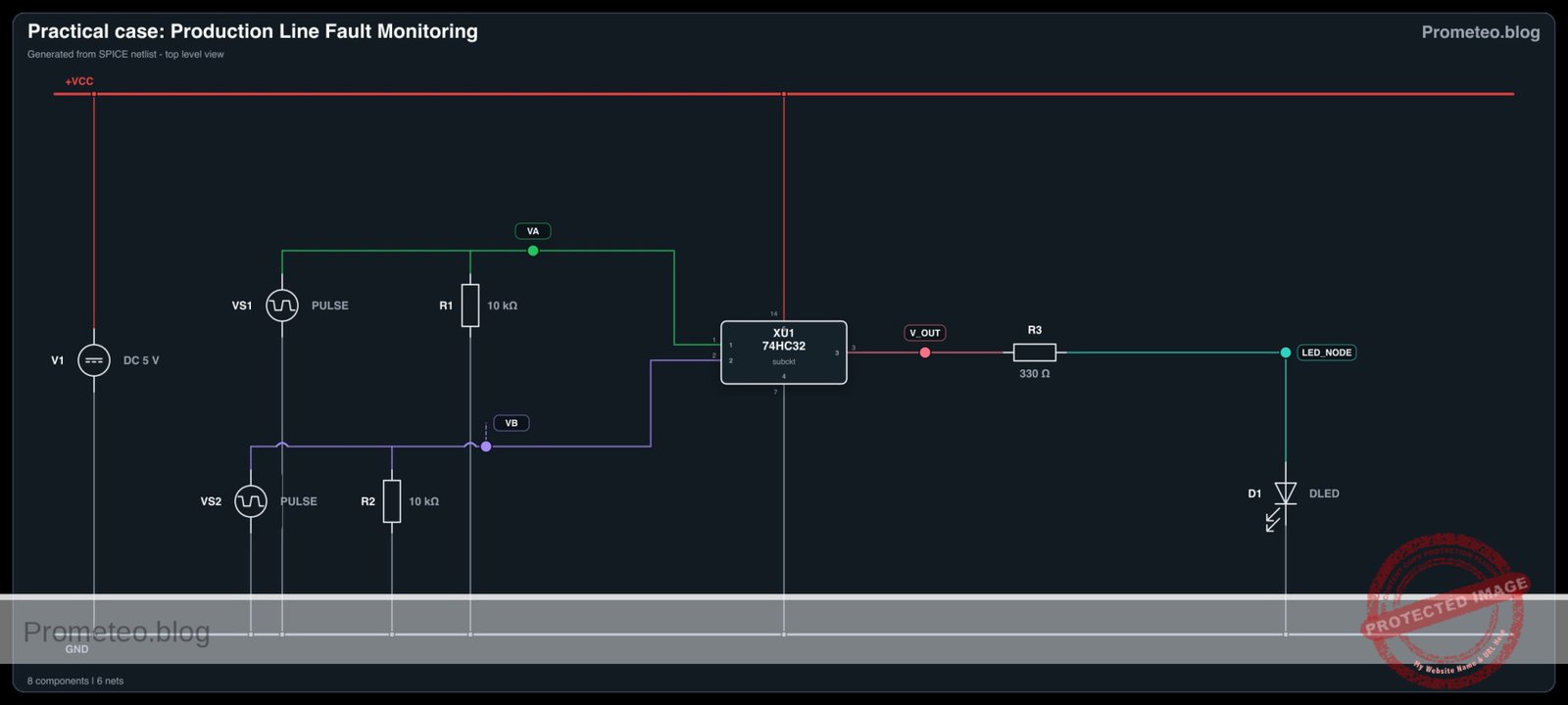
You will build a logic control circuit using an OR gate to combine signals from two distinct safety sensors (Temperature and Optical Jam). When either sensor detects a fault (Logic High), the system will output an active signal to trigger an indicator or stop mechanism.
Why it is useful:
* Industrial Safety: Prevents machinery from operating under dangerous conditions.
* Equipment Protection: Stops motors immediately if they overheat to prevent permanent damage.
* Process Efficiency: Detects physical jams on conveyor belts automatically, reducing waste.
* Redundancy: Allows multiple different error types to trigger the same emergency stop routine.
Expected outcome:
* System Standby: When both sensors are Low (0V), the output LED is OFF.
* Temperature Fault: If the temperature sensor triggers (High/5V), the LED turns ON.
* Jam Fault: If the jam sensor triggers (High/5V), the LED turns ON.
* Critical Failure: If both sensors trigger simultaneously, the LED remains ON.
Target audience and level: Electronics students and hobbyists, Level Medium.
Materials
- V1: 5 V DC power supply, function: Main circuit power.
- U1: 74HC32, function: Quad 2-input OR gate IC.
- S1: SPST Toggle Switch, function: Simulates Temperature Sensor (Open=Normal, Closed=Overheat).
- S2: SPST Toggle Switch, function: Simulates Jam Sensor (Open=Clear, Closed=Jam).
- R1: 10 kΩ resistor, function: Pull-down for Temperature Input.
- R2: 10 kΩ resistor, function: Pull-down for Jam Input.
- R3: 330 Ω resistor, function: Current limiting for indicator LED.
- D1: Red LED, function: Visual Fault Indicator.
Pin-out of the IC used
Selected Chip: 74HC32 (Quad 2-Input OR Gate)
| Pin | Name | Logic function | Connection in this case |
|---|---|---|---|
| 1 | 1A | Input A | Connected to Temperature Sensor (S1) |
| 2 | 1B | Input B | Connected to Jam Sensor (S2) |
| 3 | 1Y | Output | Connected to LED driver (R3 + D1) |
| 7 | GND | Ground | Connected to Power Supply Negative (0V) |
| 14 | VCC | Power (+) | Connected to Power Supply Positive (5V) |
Wiring guide
- VCC: Connect V1 positive terminal to U1 pin 14.
- 0 (GND): Connect V1 negative terminal to U1 pin 7.
- VA (Temp Signal): Connect S1 terminal 2 to U1 pin 1.
- VA (Temp Signal): Connect R1 between U1 pin 1 and 0.
- VCC: Connect S1 terminal 1 to VCC.
- VB (Jam Signal): Connect S2 terminal 2 to U1 pin 2.
- VB (Jam Signal): Connect R2 between U1 pin 2 and 0.
- VCC: Connect S2 terminal 1 to VCC.
- V_OUT: Connect U1 pin 3 to R3 terminal 1.
- LED_NODE: Connect R3 terminal 2 to D1 Anode.
- 0 (GND): Connect D1 Cathode to 0.
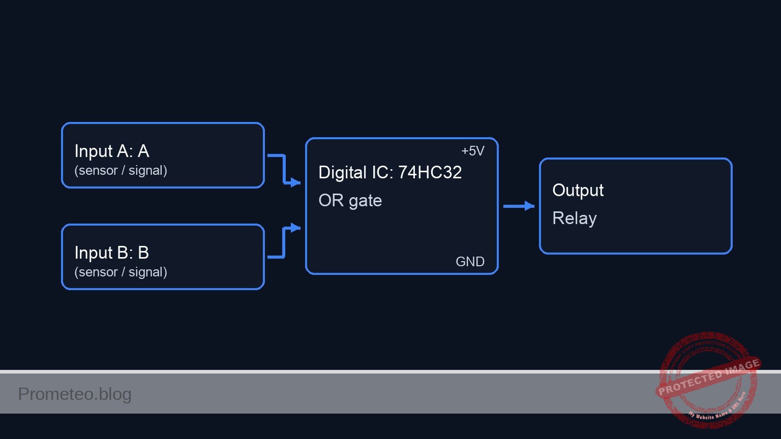
Conceptual block diagram
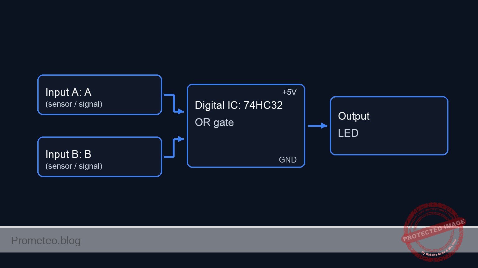
Schematic
Title: Production Line Fault Monitoring (OR Logic)

      [ INPUT SENSORS ]                       [ LOGIC PROCESSING ]                 [ VISUAL OUTPUT ]

                                                 (Pin 14: VCC)
                                                       |
                                                       v
[ VCC ] --> [ S1: Temp Switch ] --+--(Pin 1)-->+---------------+
                                  |            |               |
                             [ R1: 10k ]       |   U1: 74HC32  |
                                  |            |   (OR Gate)   |--(Pin 3)--> [ R3: 330 ] --> [ D1: LED ] --> [ GND ]
                               [ GND ]         |               |
                                               |               |
[ VCC ] --> [ S2: Jam Switch  ] --+--(Pin 2)-->+---------------+
                                  |                    ^
                             [ R2: 10k ]               |
                                  |               (Pin 7: GND)
                               [ GND ]
Electrical diagram
Truth table
This circuit utilizes positive logic (Active High).
| Sensor A (Temp) | Sensor B (Jam) | Output (Fault Indicator) | LED State |
|---|---|---|---|
| Low (0) | Low (0) | Low (0) | OFF |
| Low (0) | High (1) | High (1) | ON |
| High (1) | Low (0) | High (1) | ON |
| High (1) | High (1) | High (1) | ON |
Measurements and tests
- Standby Check: Ensure both switches S1 and S2 are open. Measure voltage at U1 Pin 3 relative to GND. It should be ~0 V. LED should be OFF.
- Temperature Fault Simulation: Close S1 while keeping S2 open. Measure voltage at Pin 1 (Input A). It should be 5 V. The Output Pin 3 should go to High (~5 V) and the LED must light up.
- Jam Fault Simulation: Open S1 and close S2. Measure voltage at Pin 2 (Input B). It should be 5 V. The LED must light up.
- Simultaneous Fault: Close both S1 and S2. The LED must remain ON.
SPICE netlist and simulation
Reference SPICE Netlist (ngspice) — excerptFull SPICE netlist (ngspice)
* Practical case: Production Line Fault Monitoring

* --- Component Models ---
* Generic Red LED Model
.model DLED D (IS=1e-14 N=2 RS=10 BV=5 IBV=10u CJO=10p)

* --- Subcircuits ---
* 74HC32 Quad 2-input OR Gate
* Pinout: 1=InputA, 2=InputB, 3=Output, 7=GND, 14=VCC
* Implemented using a robust behavioral source with continuous functions
.subckt 74HC32 1 2 3 7 14
* Logic: Output = VCC if (A > 2.5V OR B > 2.5V)
* Using sigmoid function for smooth convergence: S(x) = 1/(1+exp(-k*(x-thresh)))
* max(V(1), V(2)) selects the higher voltage to compare against threshold (2.5V)
B_OR 3 7 V = V(14) * (1 / (1 + exp(-20 * (max(V(1), V(2)) - 2.5))))
.ends

* --- Main Power Supply ---
* V1: 5V DC Supply
* Wiring: Positive -> Node 14 (VCC), Negative -> Node 0 (GND)
V1 14 0 DC 5

* --- Input Sensors (Simulated Switches) ---
* S1: Temperature Sensor Switch
* Wiring: Connects VCC to VA (Pin 1). Modeled as Pulse Source to simulate toggling.
* Logic Sequence: High (Overheat) / Low (Normal)
VS1 VA 0 PULSE(0 5 0 1u 1u 200u 400u)

* S2: Jam Sensor Switch
* Wiring: Connects VCC to VB (Pin 2). Modeled as Pulse Source with faster period.
* ... (truncated in public view) ...
Copy this content into a .cir file and run with ngspice.
* Practical case: Production Line Fault Monitoring

* --- Component Models ---
* Generic Red LED Model
.model DLED D (IS=1e-14 N=2 RS=10 BV=5 IBV=10u CJO=10p)

* --- Subcircuits ---
* 74HC32 Quad 2-input OR Gate
* Pinout: 1=InputA, 2=InputB, 3=Output, 7=GND, 14=VCC
* Implemented using a robust behavioral source with continuous functions
.subckt 74HC32 1 2 3 7 14
* Logic: Output = VCC if (A > 2.5V OR B > 2.5V)
* Using sigmoid function for smooth convergence: S(x) = 1/(1+exp(-k*(x-thresh)))
* max(V(1), V(2)) selects the higher voltage to compare against threshold (2.5V)
B_OR 3 7 V = V(14) * (1 / (1 + exp(-20 * (max(V(1), V(2)) - 2.5))))
.ends

* --- Main Power Supply ---
* V1: 5V DC Supply
* Wiring: Positive -> Node 14 (VCC), Negative -> Node 0 (GND)
V1 14 0 DC 5

* --- Input Sensors (Simulated Switches) ---
* S1: Temperature Sensor Switch
* Wiring: Connects VCC to VA (Pin 1). Modeled as Pulse Source to simulate toggling.
* Logic Sequence: High (Overheat) / Low (Normal)
VS1 VA 0 PULSE(0 5 0 1u 1u 200u 400u)

* S2: Jam Sensor Switch
* Wiring: Connects VCC to VB (Pin 2). Modeled as Pulse Source with faster period.
* Logic Sequence: High (Jam) / Low (Clear)
VS2 VB 0 PULSE(0 5 0 1u 1u 100u 200u)

* --- Pull-down Resistors ---
* R1: 10k Pull-down for Temp Input
R1 VA 0 10k
* R2: 10k Pull-down for Jam Input
R2 VB 0 10k

* --- Logic IC U1 ---
* U1: 74HC32 Quad OR Gate
* Connections per wiring guide:
* Pin 1 (A) -> VA
* Pin 2 (B) -> VB
* Pin 3 (Y) -> V_OUT
* Pin 7 (GND) -> 0
* Pin 14 (VCC) -> 14
XU1 VA VB V_OUT 0 14 74HC32

* --- Output Indicator ---
* R3: 330 Ohm Current Limiting Resistor
R3 V_OUT LED_NODE 330

* D1: Red LED Visual Indicator
* Anode -> LED_NODE, Cathode -> GND
D1 LED_NODE 0 DLED

* --- Analysis Directives ---
* Transient analysis to capture truth table states (00, 01, 10, 11)
.tran 1u 400u

* Print required voltages for verification
.print tran V(VA) V(VB) V(V_OUT) V(LED_NODE)

* Calculate DC operating point
.op

.end
Simulation Results (Transient Analysis)

Show raw data table (906 rows)
Index   time            v(va)           v(vb)           v(v_out)
0	0.000000e+00	0.000000e+00	0.000000e+00	9.643749e-22
1	1.000000e-08	5.000000e-02	5.000000e-02	1.928750e-21
2	2.000000e-08	1.000000e-01	1.000000e-01	5.242886e-21
3	4.000000e-08	2.000000e-01	2.000000e-01	2.137746e-20
4	8.000000e-08	4.000000e-01	4.000000e-01	2.632654e-19
5	1.600000e-07	8.000000e-01	8.000000e-01	2.587285e-17
6	3.200000e-07	1.600000e+00	1.600000e+00	7.614990e-08
7	4.700575e-07	2.350288e+00	2.350288e+00	2.384318e-01
8	6.126008e-07	3.063004e+00	3.063004e+00	4.999936e+00
9	7.041960e-07	3.520980e+00	3.520980e+00	5.000000e+00
10	7.932149e-07	3.966074e+00	3.966074e+00	5.000000e+00
11	9.007723e-07	4.503862e+00	4.503862e+00	5.000000e+00
12	1.000000e-06	5.000000e+00	5.000000e+00	5.000000e+00
13	1.021511e-06	5.000000e+00	5.000000e+00	5.000000e+00
14	1.064534e-06	5.000000e+00	5.000000e+00	5.000000e+00
15	1.150580e-06	5.000000e+00	5.000000e+00	5.000000e+00
16	1.322672e-06	5.000000e+00	5.000000e+00	5.000000e+00
17	1.666856e-06	5.000000e+00	5.000000e+00	5.000000e+00
18	2.355224e-06	5.000000e+00	5.000000e+00	5.000000e+00
19	3.355224e-06	5.000000e+00	5.000000e+00	5.000000e+00
20	4.355224e-06	5.000000e+00	5.000000e+00	5.000000e+00
21	5.355224e-06	5.000000e+00	5.000000e+00	5.000000e+00
22	6.355224e-06	5.000000e+00	5.000000e+00	5.000000e+00
23	7.355224e-06	5.000000e+00	5.000000e+00	5.000000e+00
... (882 more rows) ...
Common mistakes and how to avoid them
- Leaving Inputs Floating: Failing to install pull-down resistors (R1, R2) causes the inputs to «float» and pick up noise, causing the LED to flicker or stay ON randomly. Solution: Always use 10kΩ pull-down resistors on CMOS inputs connected to switches.
- Missing Current Limiting Resistor: Connecting the LED directly to the 74HC32 output pin without R3. Solution: Ensure R3 (330Ω) is in series with the LED to prevent burning out the IC or the LED.
- Confusing Pinout: Treating the 74HC32 like a different logic chip (e.g., 74HC02 NOR) due to similar package shape. Solution: Always verify the datasheet pin diagram; Pin 3 is output for the first gate on the 74HC32.
Troubleshooting
- LED is always ON: Check if pull-down resistors R1 and R2 are connected to Ground. If inputs are disconnected, they float High.
- LED is very dim: The resistor R3 might be too high (e.g., 10kΩ instead of 330Ω) or the power supply voltage is below 3V.
- Nothing happens when switches close: Verify that U1 Pin 14 is connected to 5V and Pin 7 is connected to GND. Check switch continuity.
- Logic is inverted (LED OFF when fault occurs): You may have accidentally used a NOR gate or wired the LED active-low (Anode to VCC, Cathode to Output).
Possible improvements and extensions
- Latching Alarm: Add an SR Flip-Flop or a feedback loop so that once a fault is detected, the alarm stays ON until a manual «Reset» button is pressed, even if the sensor returns to normal.
- Audible Alert: Connect a transistor driver and a 5V active buzzer in parallel with the LED to provide an audio warning for noisy factory environments.
More Practical Cases on Prometeo.blog
Find this product and/or books on this topic on Amazon
As an Amazon Associate, I earn from qualifying purchases. If you buy through this link, you help keep this project running.
Quick Quiz

Telecommunications Electronics Engineer and Computer Engineer (official degrees in Spain).