Level: Basic. Design a control system that activates a drainage pump if either of two water level sensors is triggered.
Objective and use case
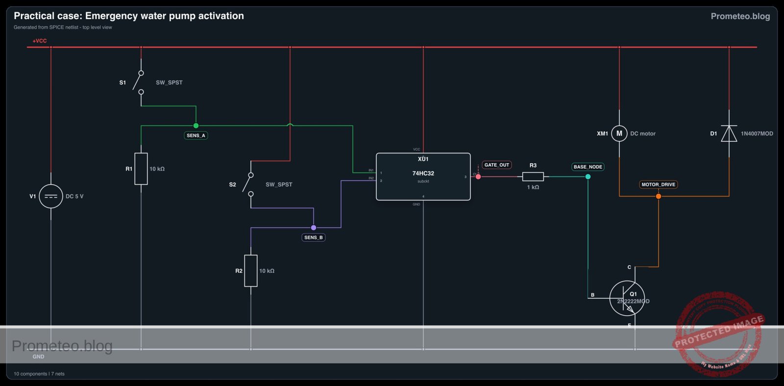
You will build a logic control circuit using a 74HC32 (OR Gate) to drive a DC motor via a transistor driver whenever water is detected by at least one sensor.
Why it is useful:
* Flood Prevention: Automatically activates a sump pump in a basement when water rises to a critical level.
* Industrial Safety: Prevents tank overflows by draining liquid if primary or secondary high-level sensors are triggered.
* Marine Applications: Activates a boat’s bilge pump if water enters the hull from either the port or starboard side.
* Redundancy: Ensures the pump starts even if one sensor fails (provided the other detects the water).
Expected outcome:
* The motor turns ON if Sensor A is HIGH.
* The motor turns ON if Sensor B is HIGH.
* The motor turns ON if both sensors are HIGH.
* The logic output at the gate pin reads ~5 V (Logic 1) when active.
* Target audience: Basic electronics students and hobbyists.
Materials
- V1: 5 V DC supply, function: Main circuit power.
- S1: SPST Switch, function: Simulates Water Level Sensor A.
- S2: SPST Switch, function: Simulates Water Level Sensor B.
- R1: 10 kΩ resistor, function: Pull-down for Sensor A.
- R2: 10 kΩ resistor, function: Pull-down for Sensor B.
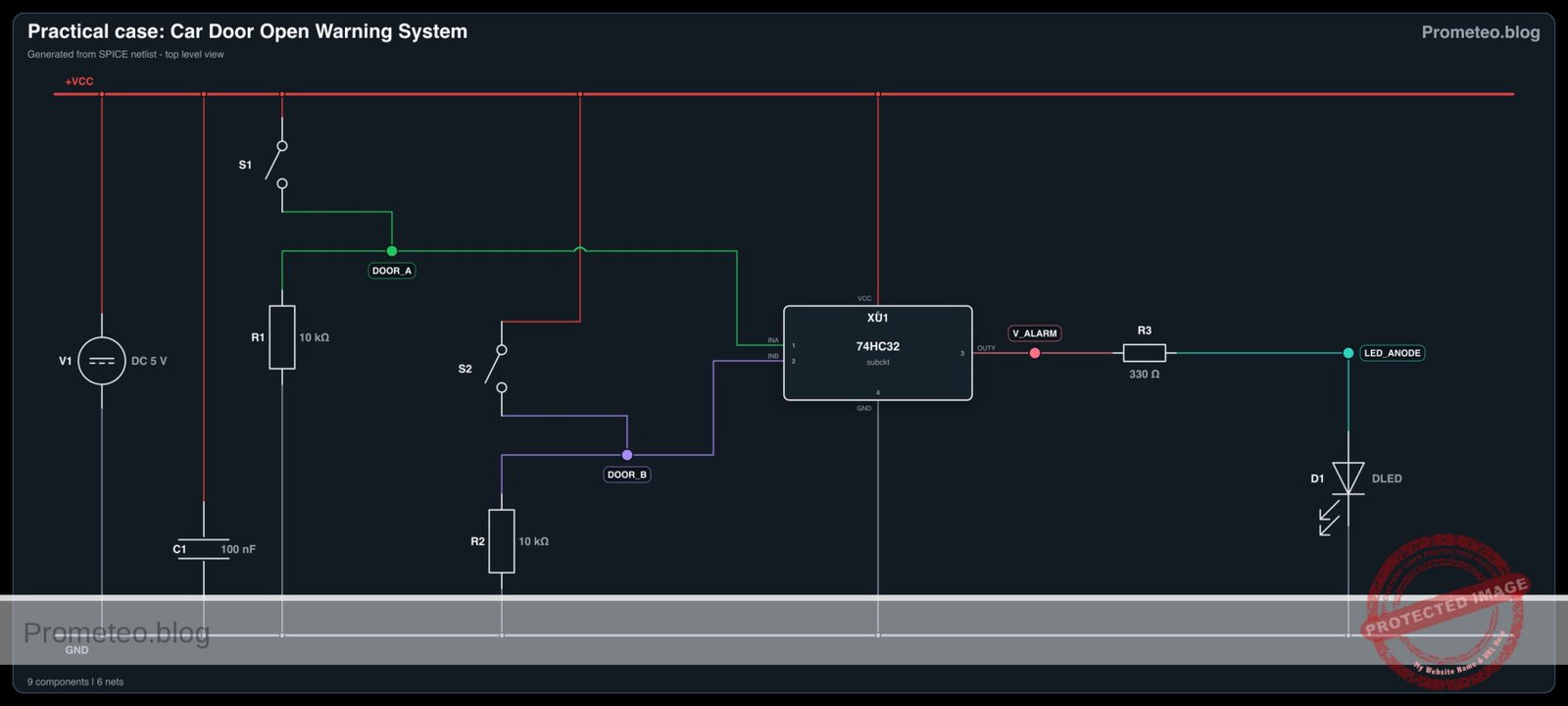
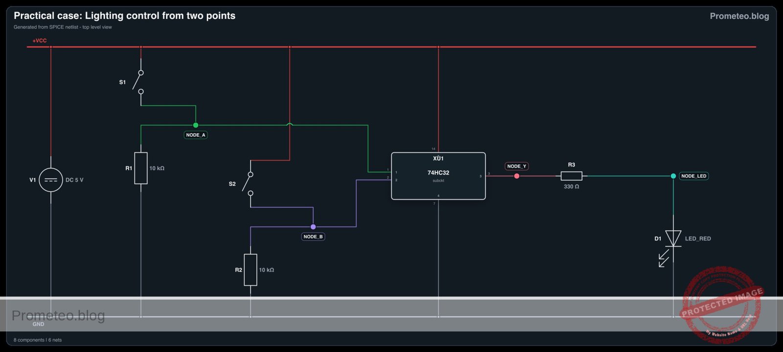
- U1: 74HC32 Quad 2-Input OR Gate.
- R3: 1 kΩ resistor, function: Transistor base current limiting.
- Q1: 2N2222 NPN Transistor, function: Motor driver switch.
- D1: 1N4007 Diode, function: Flyback protection (snubber).
- M1: 5 V DC Motor, function: Drainage pump simulation.
Pin-out of the IC used
Chip: 74HC32 (Quad 2-Input OR Gate)
| Pin | Name | Logic function | Connection in this case |
|---|---|---|---|
| 1 | 1A | Input A | Connected to Node SENS_A |
| 2 | 1B | Input B | Connected to Node SENS_B |
| 3 | 1Y | Output | Connected to Node GATE_OUT |
| 7 | GND | Ground | Connected to Node 0 (GND) |
| 14 | VCC | Power (+5V) | Connected to Node VCC |
Wiring guide
Construct the circuit following these node connections:
- VCC: Connect positive terminal of V1, one side of S1, one side of S2, Pin 14 of U1, and the positive terminal of M1.
- 0 (GND): Connect negative terminal of V1, Pin 7 of U1, Emitter of Q1, bottom of R1, and bottom of R2.
- SENS_A: Connect other side of S1, top of R1, and Pin 1 of U1.
- SENS_B: Connect other side of S2, top of R2, and Pin 2 of U1.
- GATE_OUT: Connect Pin 3 of U1 to one side of R3.
- BASE_NODE: Connect the other side of R3 to the Base of Q1.
- MOTOR_DRIVE: Connect the Collector of Q1, the negative terminal of M1, and the Anode of D1.
- PROTECTION: Connect the Cathode of D1 to VCC (Across the motor).
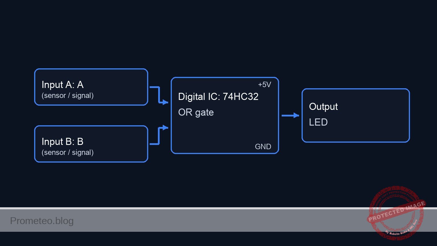
Conceptual block diagram
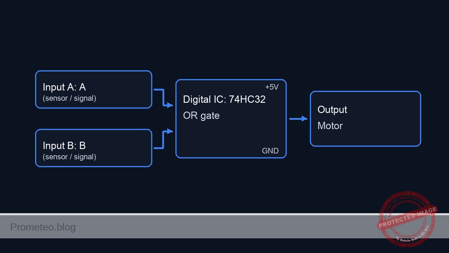
Schematic
[ INPUTS / SENSORS ]                 [ LOGIC CONTROL ]                   [ ACTUATOR / OUTPUT ]

                                          +----------------+
    [ Switch S1 ]                         |                |
    [ + R1 (PD) ] --(SENS_A / Pin 1)----->|   U1: 74HC32   |
                                          |   (OR Gate)    |
                                          |                |--(GATE_OUT / Pin 3)--> [ Resistor R3 ]
                                          |   Logic:       |                            |
    [ Switch S2 ]                         |   If A OR B    |                            |
    [ + R2 (PD) ] --(SENS_B / Pin 2)----->|   Then HIGH    |                            |
                                          |                |                      (BASE_NODE)
                                          +----------------+                            |
                                                                                        v
                                                                               [ Q1 NPN Transistor ]
                                                                               (Electronic Switch)
                                                                                        |
                                                                                        | (Switches GND)
                                                                                        |
                                                                                  (MOTOR_DRIVE)
                                                                                        |
                                                                                        v
                                                                             [ Motor M1 + Diode D1 ]
                                                                             (Connected to VCC)
Electrical diagram
Truth table
This table describes the logic state of the 74HC32 and the resulting physical action of the pump.
| Sensor A (Input 1A) | Sensor B (Input 1B) | Logic Output (Pin 1Y) | Transistor State | Pump Status |
|---|---|---|---|---|
| Low (0) | Low (0) | Low (0) | OFF (Open) | OFF |
| Low (0) | High (1) | High (1) | ON (Saturation) | ON |
| High (1) | Low (0) | High (1) | ON (Saturation) | ON |
| High (1) | High (1) | High (1) | ON (Saturation) | ON |
Measurements and tests
- Power Check: Before connecting the motor, measure the voltage between VCC and GND. It should be stable at 5 V.
- Idle State: Ensure both switches are open. Measure voltage at Pin 3 (GATE_OUT). It should be ~0 V. The motor should be stopped.
- Sensor A Activation: Close S1. Measure voltage at Pin 1 (Input A). It should be 5 V. Pin 3 should go High, and the motor should spin.
- Sensor B Activation: Open S1 and close S2. Verify the motor spins.
- Simultaneous Activation: Close both S1 and S2. The motor should remain spinning.
- Current Draw: Place an ammeter in series with the motor. Note the current consumption (typically 50mA to 200mA for small hobby motors).
SPICE netlist and simulation
Reference SPICE Netlist (ngspice) — excerptFull SPICE netlist (ngspice)
* Emergency water pump activation fixed

* --- Power Supply ---
V1 VCC 0 DC 5

* --- Switches & Sensors ---
* S1: Simulates Water Level Sensor A
V_ACT_A ACT_A 0 PULSE(0 5 0 1u 1u 1m 2m)
S1 VCC SENS_A ACT_A 0 SW_MOD

* R1: Pull-down for Sensor A
R1 SENS_A 0 10k

* S2: Simulates Water Level Sensor B
V_ACT_B ACT_B 0 PULSE(0 5 0 1u 1u 0.5m 1m)
S2 VCC SENS_B ACT_B 0 SW_MOD

* R2: Pull-down for Sensor B
R2 SENS_B 0 10k

* --- Logic Gate U1: 74HC32 (Quad OR) ---
* Pin 1: SENS_A, Pin 2: SENS_B, Pin 3: GATE_OUT, Pin 7: GND, Pin 14: VCC
XU1 SENS_A SENS_B GATE_OUT 0 VCC 74HC32_GATE

* --- Driver Stage ---
* R3: Base resistor
R3 GATE_OUT BASE_NODE 1k

* Q1: NPN Transistor Switch
* Collector: MOTOR_DRIVE, Base: BASE_NODE, Emitter: 0 (GND)
* ... (truncated in public view) ...
Copy this content into a .cir file and run with ngspice.
* Emergency water pump activation fixed

* --- Power Supply ---
V1 VCC 0 DC 5

* --- Switches & Sensors ---
* S1: Simulates Water Level Sensor A
V_ACT_A ACT_A 0 PULSE(0 5 0 1u 1u 1m 2m)
S1 VCC SENS_A ACT_A 0 SW_MOD

* R1: Pull-down for Sensor A
R1 SENS_A 0 10k

* S2: Simulates Water Level Sensor B
V_ACT_B ACT_B 0 PULSE(0 5 0 1u 1u 0.5m 1m)
S2 VCC SENS_B ACT_B 0 SW_MOD

* R2: Pull-down for Sensor B
R2 SENS_B 0 10k

* --- Logic Gate U1: 74HC32 (Quad OR) ---
* Pin 1: SENS_A, Pin 2: SENS_B, Pin 3: GATE_OUT, Pin 7: GND, Pin 14: VCC
XU1 SENS_A SENS_B GATE_OUT 0 VCC 74HC32_GATE

* --- Driver Stage ---
* R3: Base resistor
R3 GATE_OUT BASE_NODE 1k

* Q1: NPN Transistor Switch
* Collector: MOTOR_DRIVE, Base: BASE_NODE, Emitter: 0 (GND)
Q1 MOTOR_DRIVE BASE_NODE 0 2N2222MOD

* --- Output Load (Motor) ---
* M1: 5V DC Motor simulation (Inductive Load)
* Fixed: Subcircuit name changed from DC_MOTOR_MODEL to DC_MOTOR to match definition
XM1 VCC MOTOR_DRIVE DC_MOTOR

* --- Protection ---
* D1: Flyback Diode
D1 MOTOR_DRIVE VCC 1N4007MOD

* --- Models and Subcircuits ---

* Switch Model
.model SW_MOD SW(Vt=2.5 Vh=0.1 Ron=0.1 Roff=10Meg)

* Transistor Model (Generic 2N2222)
.model 2N2222MOD NPN(Is=14.34f Xti=3 Eg=1.11 Vaf=74.03 Bf=255.9 Ne=1.307 Ise=14.34f Ikf=.2847 Xtb=1.5 Br=6.092 Nc=2 Isc=0 Ikr=0 Rc=1 Cjc=7.306p Mjc=.3416 Vjc=.75 Fc=.5 Cje=22.01p Mje=.377 Vje=.75 Tr=46.91n Tf=411.1p Itf=.6 Vtf=1.7 Xtf=3 Rb=10)

* Diode Model (Generic 1N4007)
.model 1N4007MOD D(IS=7.027n RS=0.03415 N=1.267 EG=1.11 XTI=3 BV=1000 IBV=10m CJO=10p VJ=0.7 M=0.5 FC=0.5 TT=100n)

* Motor Model (Simple RL series)
.subckt DC_MOTOR POS NEG
Rcoil POS INT 50
Lcoil INT NEG 5m
.ends

* 74HC32 Logic Gate Model (Behavioral)
* Implements OR logic: OUT = 1 if (IN1=1 OR IN2=1)
.subckt 74HC32_GATE IN1 IN2 OUT GND VCC
B_OR OUT GND V=V(VCC) * ( (1/(1+exp(-20*(V(IN1)-2.5)))) + (1/(1+exp(-20*(V(IN2)-2.5)))) - ( (1/(1+exp(-20*(V(IN1)-2.5)))) * (1/(1+exp(-20*(V(IN2)-2.5)))) ) )
.ends

* --- Simulation Directives ---
.tran 10u 2.5m

* Print required nodes for validation
.print tran V(SENS_A) V(SENS_B) V(GATE_OUT) V(BASE_NODE) V(MOTOR_DRIVE)

.end
Simulation Results (Transient Analysis)

Show raw data table (2750 rows)
Index   time            v(sens_a)       v(sens_b)       v(gate_out)
0	0.000000e+00	4.995005e-03	4.995005e-03	2.131385e-21
1	1.000000e-08	4.995005e-03	4.995005e-03	2.131385e-21
2	2.000000e-08	4.995005e-03	4.995005e-03	2.131385e-21
3	4.000000e-08	4.995005e-03	4.995005e-03	2.131385e-21
4	8.000000e-08	4.995005e-03	4.995005e-03	2.131385e-21
5	1.600000e-07	4.995005e-03	4.995005e-03	2.131385e-21
6	3.200000e-07	4.995005e-03	4.995005e-03	2.131385e-21
7	3.600000e-07	4.995005e-03	4.995005e-03	2.131385e-21
8	4.300000e-07	4.995005e-03	4.995005e-03	2.131385e-21
9	4.493750e-07	4.995005e-03	4.995005e-03	2.131385e-21
10	4.832812e-07	4.995005e-03	4.995005e-03	2.131385e-21
11	5.162979e-07	4.999950e+00	4.999950e+00	5.000000e+00
12	5.395702e-07	4.999950e+00	4.999950e+00	5.000000e+00
13	5.611432e-07	4.999950e+00	4.999950e+00	5.000000e+00
14	5.884211e-07	4.999950e+00	4.999950e+00	5.000000e+00
15	6.429769e-07	4.999950e+00	4.999950e+00	5.000000e+00
16	7.520886e-07	4.999950e+00	4.999950e+00	5.000000e+00
17	9.703119e-07	4.999950e+00	4.999950e+00	5.000000e+00
18	1.000000e-06	4.999950e+00	4.999950e+00	5.000000e+00
19	1.030157e-06	4.999950e+00	4.999950e+00	5.000000e+00
20	1.090472e-06	4.999950e+00	4.999950e+00	5.000000e+00
21	1.211102e-06	4.999950e+00	4.999950e+00	5.000000e+00
22	1.452361e-06	4.999950e+00	4.999950e+00	5.000000e+00
23	1.934879e-06	4.999950e+00	4.999950e+00	5.000000e+00
... (2726 more rows) ...
Common mistakes and how to avoid them
- Floating Inputs: Forgetting the pull-down resistors (R1, R2).
- Solution: Always connect inputs to ground via a resistor (10kΩ) so they default to 0 V when switches are open.
- Missing Flyback Diode: Omitting D1 across the motor.
- Solution: Inductive loads generate voltage spikes when turned off. Always place a diode in reverse bias across the motor to protect the transistor.
- Overloading the Gate: Connecting the motor directly to the 74HC32 output pin.
- Solution: Logic gates can only supply small currents (~20mA). Use a transistor (Q1) to handle the higher current required by the motor.
Troubleshooting
- Symptom: Motor runs continuously even when switches are open.
- Cause: Inputs are floating or the transistor is shorted.
- Fix: Check R1/R2 connections or replace Q1.
- Symptom: IC gets very hot immediately.
- Cause: VCC and GND pins are reversed or shorted.
- Fix: Disconnect power immediately and verify Pin 14 and Pin 7 wiring.
- Symptom: Logic output is High (5V), but motor does not spin.
- Cause: Base resistor (R3) too high or transistor gain too low.
- Fix: Verify R3 is 1kΩ. Ensure the motor power supply is adequate.
Possible improvements and extensions
- Visual Indicators: Add an LED with a current-limiting resistor in parallel with the motor to provide a visual warning when the pump is active.
- Hysteresis/Latching: Replace the OR gate with an SR Latch logic. This would keep the pump running even if the water level drops momentarily, ensuring a full drain cycle until a bottom sensor resets it.
More Practical Cases on Prometeo.blog
Find this product and/or books on this topic on Amazon
As an Amazon Associate, I earn from qualifying purchases. If you buy through this link, you help keep this project running.
Quick Quiz

Telecommunications Electronics Engineer and Computer Engineer (official degrees in Spain).