Level: Basic. Demonstrate how moving a magnet through a coil generates an electromotive force (EMF).
Objective and use case
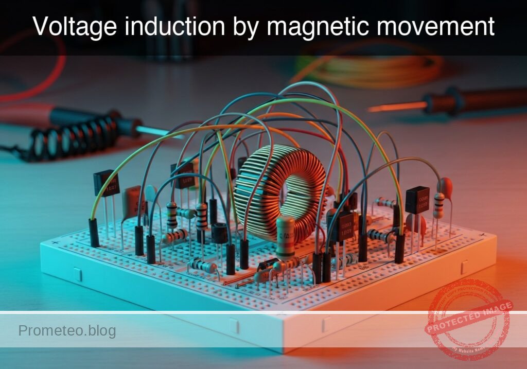
In this practical case, you will construct a fundamental electromagnetic induction demonstrator using a hand-wound copper coil and a high-strength neodymium magnet. You will observe how kinetic energy is converted into electrical energy via Faraday’s Law of Induction.
Why it is useful:
* Power Generation: This mechanism illustrates the core principle behind electric generators, alternators, and wind turbines.
* Audio Technology: This is the operating principle for dynamic microphones and electric guitar pickups (transducers).
* Sensors: Used in automotive ABS speed sensors and industrial position sensors.
* Wireless Charging: Demonstrates the basics of magnetic coupling used in phone chargers.
Expected outcome:
* A measurable voltage spike (positive or negative) on the multimeter when the magnet moves relative to the coil.
* The LED flashes briefly when the magnet is moved rapidly, indicating a voltage peak exceeding the diode’s forward voltage (~1.8 V).
* Reversing the direction of the magnet’s movement reverses the polarity of the induced voltage.
Target audience: Students and hobbyists introducing themselves to Faraday’s Law and passive components.
Materials
- L1: Air core coil (approx. 500–1000 turns of enameled copper wire), function: induction element.
- MAG1: Cylindrical Neodymium magnet (fit to pass inside L1), function: source of magnetic flux.
- D1: Red LED, function: indicator for positive phase induction.
- D2: Green LED, function: indicator for negative phase induction (connected in anti-parallel).
- M1: Multimeter (set to 200 mV or 2 V DC range), function: voltage monitor.
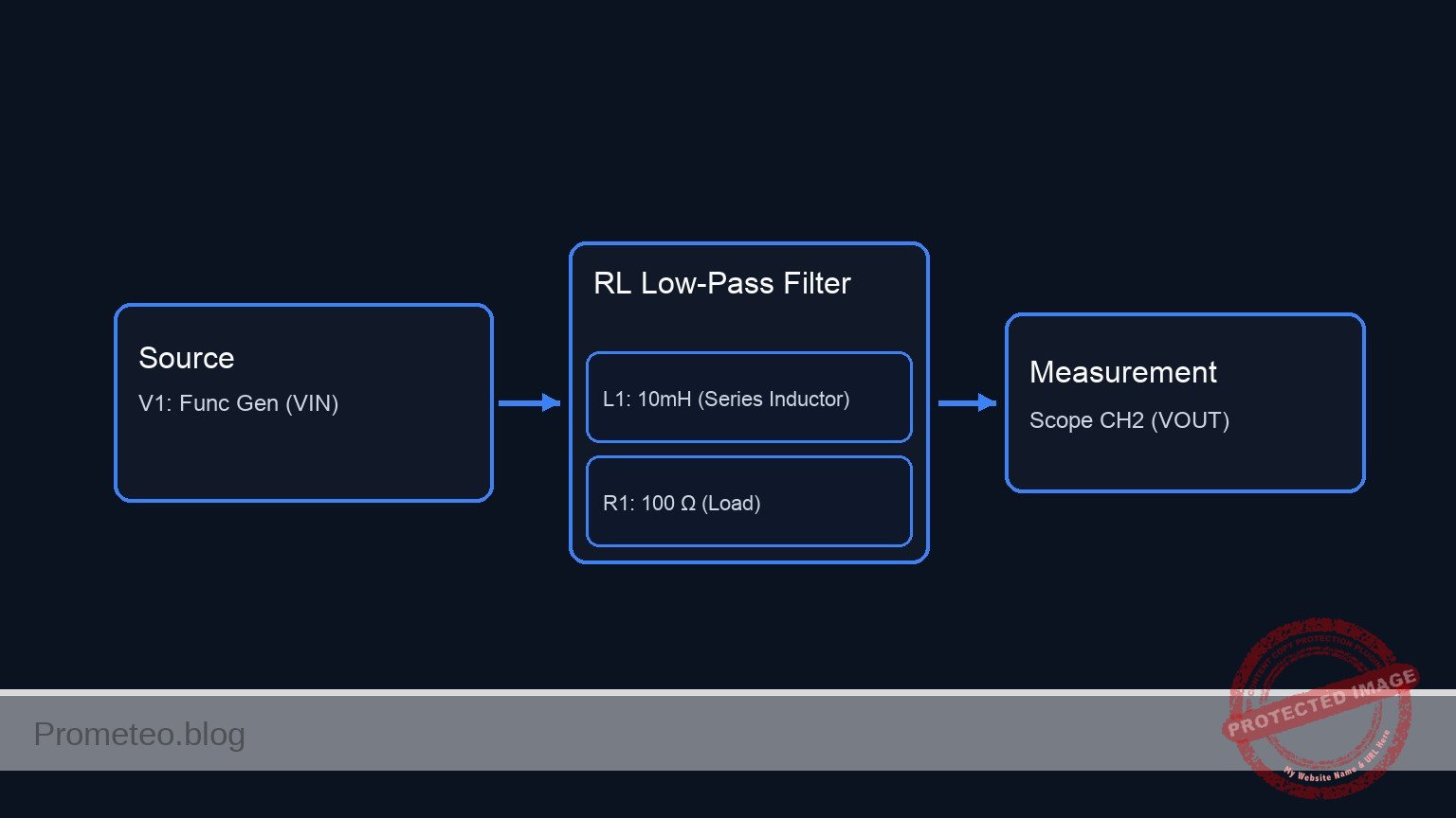
Wiring guide
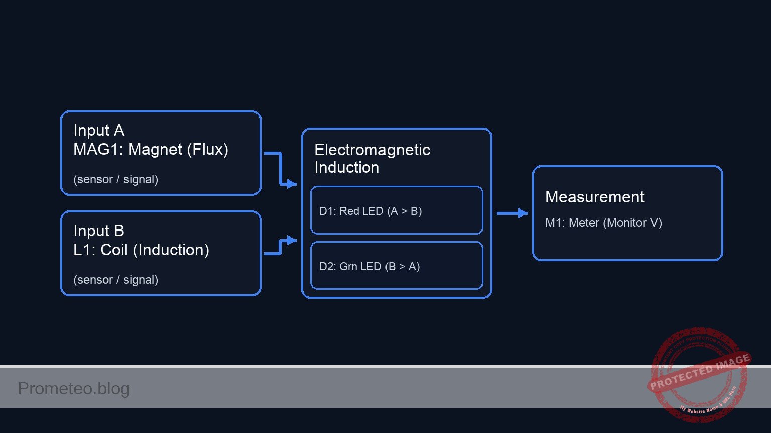
The circuit consists of the coil connected directly to the indicators in parallel. We define the coil terminals as nodes COIL_A and COIL_B.
- L1: Connects between node
COIL_Aand nodeCOIL_B. - D1: Anode connects to
COIL_A; Cathode connects toCOIL_B. - D2: Anode connects to
COIL_B; Cathode connects toCOIL_A(anti-parallel to D1). - M1: Positive probe connects to
COIL_A; Negative probe connects toCOIL_B.
Conceptual block diagram
Schematic
markdown
Title: Practical case: Voltage induction by magnetic movement

[ INPUT / SOURCE ]                       [ DISTRIBUTION RAILS ]                    [ OUTPUT / LOADS ]

                                                 (Node A: Top Rail)
                                    /------------------------------------------------------------------>
                                    |                |                    |                    |
[ MAG1: Magnet ] --(Flux)--> [ L1: Coil ]            | (Anode)            | (Cathode)          | (+)
                                    |                v                    v                    v
                                    |        [ D1: Red LED ]      [ D2: Grn LED ]      [ M1: Meter ]
                                    |        (Lights if A > B)    (Lights if B > A)    (Monitor V)
                                    |                |                    |                    |
                                    |                | (Cathode)          | (Anode)            | (-)
                                    \                v                    v                    v
                                    \------------------------------------------------------------------>
                                                 (Node B: Bottom Rail)
Electrical diagram
Measurements and tests
- Static Test: Place the magnet inside the coil and hold it completely still. The multimeter should read 0 V, and no LEDs should light up. This confirms that a changing magnetic field is required.
- Slow Insertion: Set the multimeter to the lowest DC voltage range (e.g., 200 mV). Slowly push the magnet into the coil. Observe a small voltage reading (e.g., +10 to +50 mV).
- Fast Action: Quickly thrust the magnet into the coil. You should see a significantly higher voltage spike (potentially > 1 V) and D1 (Red) may flash briefly.
- Reverse Motion: Quickly pull the magnet out of the coil. The voltage polarity on the multimeter will flip (negative sign), and D2 (Green) should flash.
- Oscillation: Move the magnet back and forth rapidly inside the coil. The LEDs should flicker alternately, demonstrating the generation of Alternating Current (AC).
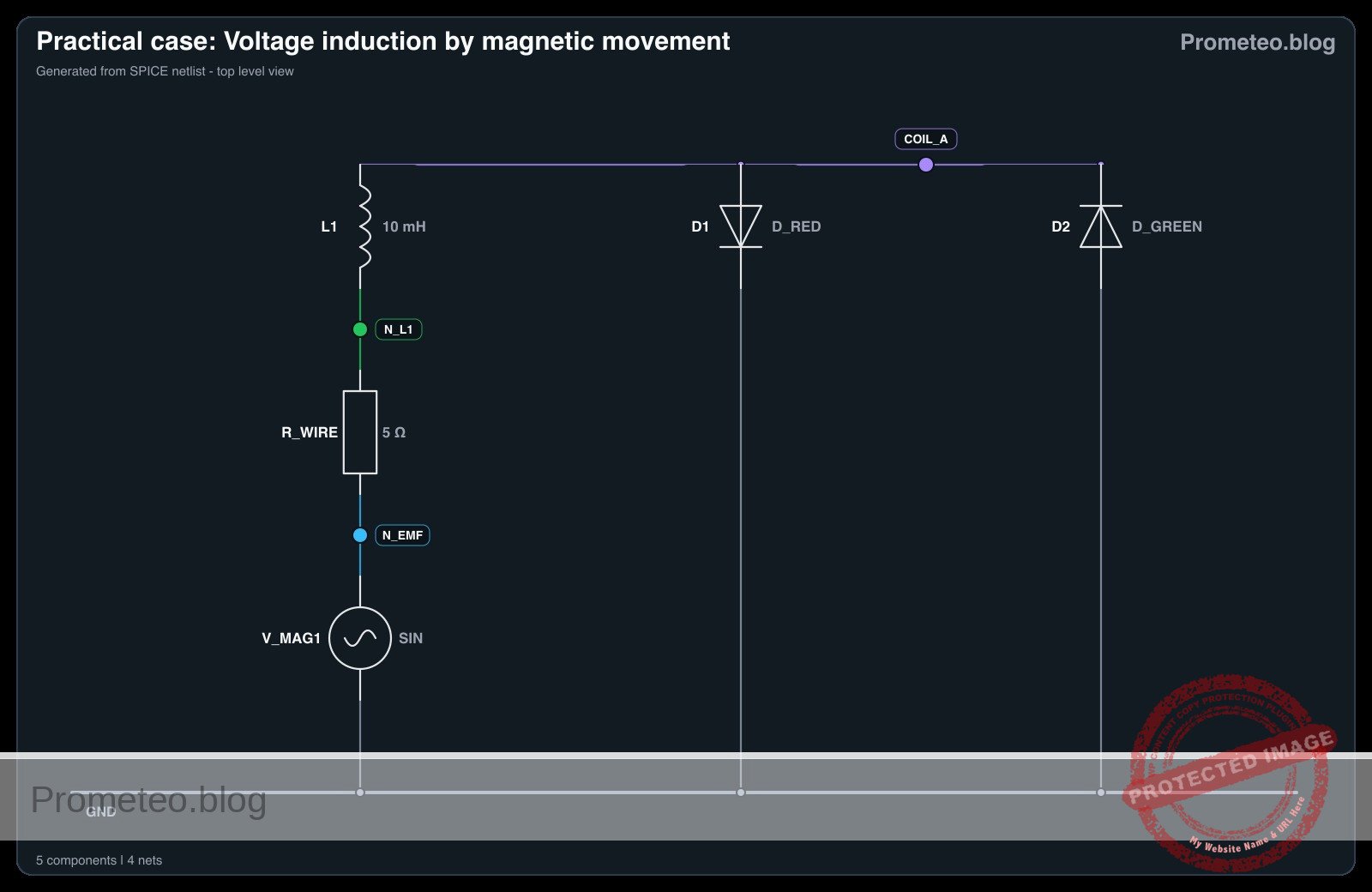
SPICE netlist and simulation
Reference SPICE Netlist (ngspice) — excerptFull SPICE netlist (ngspice)
* Practical case: Voltage induction by magnetic movement
.width out=256
*
* Description:
* Simulation of a magnet moving through a coil, inducing voltage to drive two antiparallel LEDs.
*
* Nodes:
* COIL_A : Hot terminal of the coil (Multimeter +)
* COIL_B : Reference terminal of the coil (Multimeter -, Grounded)
*
* Note: The physical "Coil" is modeled as a series combination of an EMF Voltage Source (V_MAG1),
* a Resistor (R_WIRE), and the Inductor (L1).

* --- Power / Reference ---
* Grounding COIL_B as per Multimeter negative probe convention
V_REF COIL_B 0 0

* --- Magnetic Induction Source (MAG1) ---
* Simulating the changing magnetic flux from MAG1 as an AC voltage source.
* 3V Peak, 5Hz (Simulates shaking the magnet)
* ... (truncated in public view) ...
Copy this content into a .cir file and run with ngspice.
* Practical case: Voltage induction by magnetic movement
.width out=256
*
* Description:
* Simulation of a magnet moving through a coil, inducing voltage to drive two antiparallel LEDs.
*
* Nodes:
* COIL_A : Hot terminal of the coil (Multimeter +)
* COIL_B : Reference terminal of the coil (Multimeter -, Grounded)
*
* Note: The physical "Coil" is modeled as a series combination of an EMF Voltage Source (V_MAG1),
* a Resistor (R_WIRE), and the Inductor (L1).

* --- Power / Reference ---
* Grounding COIL_B as per Multimeter negative probe convention
V_REF COIL_B 0 0

* --- Magnetic Induction Source (MAG1) ---
* Simulating the changing magnetic flux from MAG1 as an AC voltage source.
* 3V Peak, 5Hz (Simulates shaking the magnet)
V_MAG1 N_EMF COIL_B SIN(0 3 5)

* --- Coil Assembly (L1) ---
* Internal wire resistance
R_WIRE N_EMF N_L1 5
* The physical inductance L1
L1 N_L1 COIL_A 10m

* --- Indicators ---
* D1: Red LED (Indicates Positive Phase)
* Anode: COIL_A, Cathode: COIL_B
D1 COIL_A COIL_B D_RED

* D2: Green LED (Indicates Negative Phase)
* Anode: COIL_B, Cathode: COIL_A
D2 COIL_B COIL_A D_GREEN

* --- Multimeter (M1) ---
* Modeled as the voltage difference V(COIL_A) - V(COIL_B)
* (Implicit in the node voltages)

* --- Models ---
* Generic LED Models
.model D_RED D(IS=1e-18 N=2 RS=10 BV=5)
.model D_GREEN D(IS=1e-18 N=2.5 RS=10 BV=5)

* --- Simulation Directives ---
.op
* Transient analysis: 1ms step, 500ms duration (2.5 cycles at 5Hz)
.tran 1m 500m

* --- Output ---
* Monitoring the induced voltage at COIL_A
.print tran V(COIL_A) I(L1)
Simulation Results (Transient Analysis)

Show raw data table (522 rows)
Index   time            v(coil_a)       l1#branch
0	0.000000e+00	4.375392e-35	-8.75078e-36
1	1.000000e-05	9.424778e-04	1.884985e-15
2	2.000000e-05	1.884955e-03	3.769970e-15
3	4.000000e-05	3.769910e-03	7.539938e-15
4	8.000000e-05	7.539814e-03	1.507987e-14
5	1.600000e-04	1.507958e-02	3.015936e-14
6	3.200000e-04	3.015878e-02	6.031856e-14
7	6.400000e-04	6.031451e-02	1.206316e-13
8	1.280000e-03	1.206046e-01	2.412214e-13
9	2.280000e-03	2.147012e-01	4.294658e-13
10	3.280000e-03	3.085859e-01	6.175653e-13
11	4.280000e-03	4.021661e-01	8.067202e-13
12	5.280000e-03	4.953494e-01	1.005111e-12
13	6.280000e-03	5.880438e-01	1.262566e-12
14	7.280000e-03	6.801579e-01	1.873422e-12
15	8.280000e-03	7.716008e-01	4.548512e-12
16	9.280000e-03	8.622822e-01	1.907006e-11
17	1.028000e-02	9.521126e-01	1.003825e-10
18	1.128000e-02	1.041003e+00	5.511221e-10
19	1.228000e-02	1.128867e+00	3.003086e-09
20	1.328000e-02	1.215616e+00	1.605415e-08
21	1.428000e-02	1.301164e+00	8.389370e-08
22	1.528000e-02	1.385424e+00	4.276266e-07
23	1.628000e-02	1.468291e+00	2.121308e-06
... (498 more rows) ...
Reference SPICE netlist (ngspice)
* Practical case: Voltage induction by magnetic movement
.width out=256
*
* Description:
* Simulation of a magnet moving through a coil, inducing voltage to drive two antiparallel LEDs.
*
* Nodes:
* COIL_A : Hot terminal of the coil (Multimeter +)
* COIL_B : Reference terminal of the coil (Multimeter -, Grounded)
*
* Note: The physical "Coil" is modeled as a series combination of an EMF Voltage Source (V_MAG1),
* a Resistor (R_WIRE), and the Inductor (L1).

* --- Power / Reference ---
* Grounding COIL_B as per Multimeter negative probe convention
V_REF COIL_B 0 0

* --- Magnetic Induction Source (MAG1) ---
* Simulating the changing magnetic flux from MAG1 as an AC voltage source.
* 3V Peak, 5Hz (Simulates shaking the magnet)
V_MAG1 N_EMF COIL_B SIN(0 3 5)

* --- Coil Assembly (L1) ---
* Internal wire resistance
R_WIRE N_EMF N_L1 5
* The physical inductance L1
L1 N_L1 COIL_A 10m

* --- Indicators ---
* D1: Red LED (Indicates Positive Phase)
* Anode: COIL_A, Cathode: COIL_B
D1 COIL_A COIL_B D_RED

* D2: Green LED (Indicates Negative Phase)
* Anode: COIL_B, Cathode: COIL_A
D2 COIL_B COIL_A D_GREEN

* --- Multimeter (M1) ---
* Modeled as the voltage difference V(COIL_A) - V(COIL_B)
* (Implicit in the node voltages)

* --- Models ---
* Generic LED Models
.model D_RED D(IS=1e-18 N=2 RS=10 BV=5)
.model D_GREEN D(IS=1e-18 N=2.5 RS=10 BV=5)

* --- Simulation Directives ---
.op
* Transient analysis: 1ms step, 500ms duration (2.5 cycles at 5Hz)
.tran 1m 500m

* --- Output ---
* Monitoring the induced voltage at COIL_A
.print tran V(COIL_A) I(L1)
Simulation Results (Transient Analysis)
Common mistakes and how to avoid them
- Using weak magnets: Standard black ferrite magnets are often too weak to generate visible voltage on an LED. Solution: Use rare-earth Neodymium magnets.
- Moving too slowly: Faraday’s Law (V = – N · d\Phi / dt) depends on the rate of change. Solution: Move the magnet as quickly as possible to maximize the voltage spike.
- Insulation issues: Enameled wire has a clear coating that blocks electricity. Solution: Ensure the ends of the coil wire are sanded or scraped down to bare copper before connecting to the LEDs or multimeter.
Troubleshooting
- Symptom: Multimeter shows voltage, but LEDs never light up.
- Cause: The induced voltage is lower than the LED forward voltage threshold (~1.8 V).
- Fix: Add more turns to the coil (increase $N$) or move the magnet faster.
- Symptom: No reading on the multimeter even with fast movement.
- Cause: Open circuit or poor connection at the coil tips.
- Fix: Check continuity (resistance mode) across the coil terminals; it should read a few Ohms, not infinite.
- Symptom: Voltage reading is erratic or hard to see.
- Cause: Digital multimeters have a slow sample rate.
- Fix: Use the «Max/Min» hold function if available, or use an analog (needle) multimeter which responds better to transient pulses.
Possible improvements and extensions
- Shake Flashlight: Add a bridge rectifier (4 diodes) and a large capacitor (e.g., 1000 µF) to store the energy generated by shaking the magnet, allowing the LED to stay lit for a few seconds after motion stops.
- Core Comparison: Insert an iron bolt inside the coil (making it an iron-core inductor) and move a magnet near the head of the bolt to observe how the ferromagnetic core concentrates the magnetic flux and affects induction.
More Practical Cases on Prometeo.blog
Find this product and/or books on this topic on Amazon
As an Amazon Associate, I earn from qualifying purchases. If you buy through this link, you help keep this project running.
Quick Quiz

Telecommunications Electronics Engineer and Computer Engineer (official degrees in Spain).