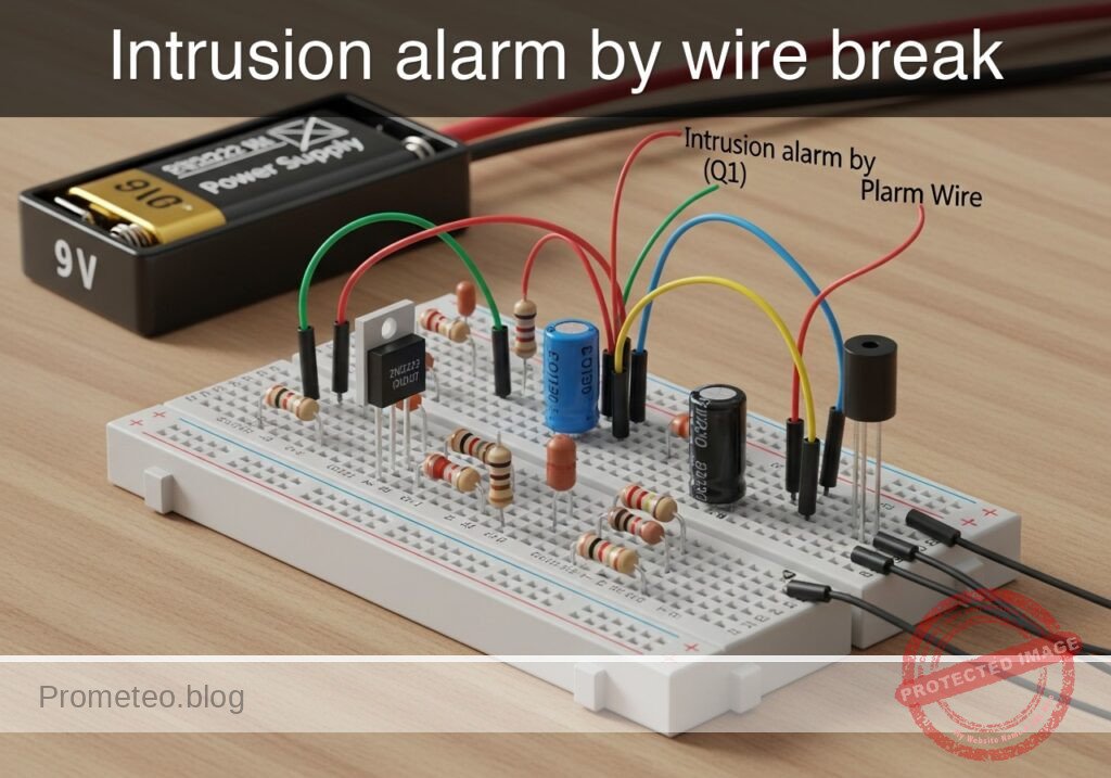
Level: Basic. Design a security circuit where cutting a wire activates an alarm using transistor saturation logic.
Objective and use case
In this project, you will build a closed-loop security system using a BJT transistor. When a specific wire (the «sense loop») is intact, the system remains silent; if the wire is cut or disconnected, an LED lights up immediately.
- Perimeter security: Monitor windows or fences where a conductive strip or wire is installed.
- Anti-tamper mechanisms: Detect if a device case has been opened by breaking a connection.
- Continuity testing: Verify cable integrity in manufacturing harnesses.
Expected outcome:
* Loop Intact (Secure): The LED remains OFF. VBE ≈ 0 V.
* Loop Cut (Alarm): The LED turns ON. VBE ≈ 0.7 V and the transistor enters saturation (VCE < 0.2 V).
Target audience: Students and hobbyists learning basic transistor switching applications.
Materials
- V1: 9 V DC power supply or battery.
- Q1: 2N2222 or BC547 (NPN BJT), function: electronic switch.
- R1: 10 kΩ resistor, function: base pull-up resistor.
- R2: 470 Ω resistor, function: LED current limiting.
- D1: Red LED, function: visual alarm indicator.
- W1: Copper wire or jumper, function: sense loop (the «intruder» wire).
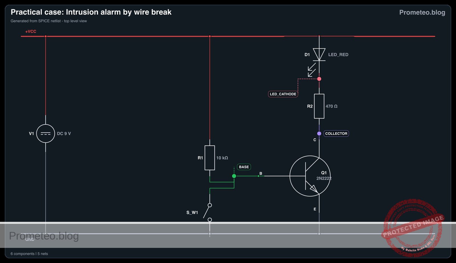
Wiring guide
Construct the circuit ensuring all connections map to the following nodes: VCC, GND (0), BASE, and COLLECTOR.
- V1: Positive terminal to
VCC, Negative terminal toGND. - R1 (Pull-up): Connects between
VCCandBASE. - W1 (Sense Loop): Connects between
BASEandGND. - Q1 (Transistor):
- Base pin to
BASE. - Emitter pin to
GND. - Collector pin to
COLLECTOR.
- Base pin to
- D1 (LED): Anode to
VCC, Cathode to nodeLED_CATHODE. - R2 (Limiting): Connects between
LED_CATHODEandCOLLECTOR.
Conceptual block diagram
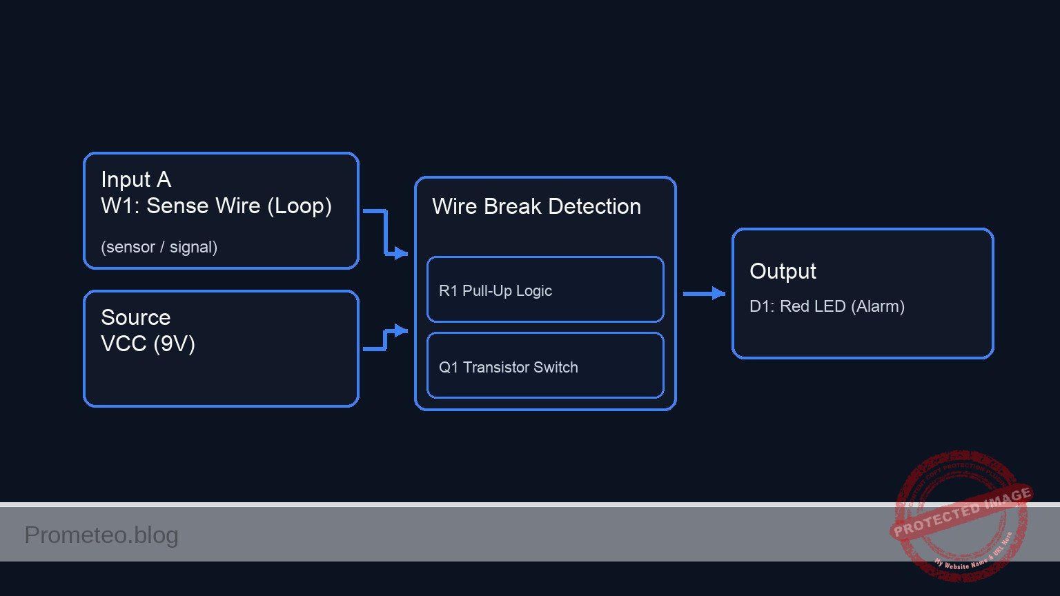
Schematic
Title: Practical case: Intrusion alarm by wire break

[ A. CONTROL / SENSING LOOP ]
(Logic: W1 keeps Base LOW. If W1 breaks, R1 pulls Base HIGH)

VCC (9 V) --> [ R1: 10k Pull-Up ] --(Node: BASE)--> [ Q1: Base ]
                                         |
                                         +-------> [ W1: Sense Wire ] --> GND


[ B. ALARM / POWER LOOP ]
(Logic: Current flows through LED only when Q1 is ON)

VCC (9 V) --> [ D1: Red LED ] --> [ R2: 470R ] --> [ Q1: Collector ]
                                                          |
                                                      (Switch)
                                                          |
                                                          v
                                                   [ Q1: Emitter ] --> GND
Electrical diagram
Measurements and tests
Verify the logic states using a multimeter.
-
State 1: Loop Intact (Secure)
- Ensure the wire W1 connects
BASEtoGND. - Measure Voltage Base-Emitter (VBE): Should be 0 V.
- Measure Voltage Collector-Emitter (VCE): Should be close to 9 V (Cut-off region).
- Result: LED is OFF.
- Ensure the wire W1 connects
-
State 2: Loop Broken (Alarm)
- Disconnect or cut wire W1.
- Measure Voltage Base-Emitter (VBE): Should be approximately 0.7 V.
- Measure Voltage Collector-Emitter (VCE): Should be approximately 0.1 V to 0.2 V (Saturation region).
- Result: LED is ON.
SPICE netlist and simulation
Reference SPICE Netlist (ngspice) — excerptFull SPICE netlist (ngspice)
* Practical case: Intrusion alarm by wire break
.width out=256

* --- Power Supply ---
* V1: 9 V DC power supply
V1 VCC 0 DC 9

* --- Input / Sense Loop ---
* W1: Sense Loop (Copper wire).
* Modeled as a Voltage Controlled Switch (S_W1) to simulate the wire breaking.
* Logic: High Control (5V) = Wire Intact (Closed). Low Control (0V) = Wire Broken (Open).
S_W1 BASE 0 CTRL 0 SW_WIRE
.model SW_WIRE SW(Vt=2.5 Vh=0.1 Ron=0.01 Roff=100Meg)

* Control Signal for W1:
* Starts at 5V (Intact), breaks at 2ms (0V), stays broken for duration.
V_W1_CTRL CTRL 0 PULSE(5 0 2ms 1u 1u 5ms 10ms)

* --- Pull-up Network ---
* R1: Base pull-up resistor
* ... (truncated in public view) ...
Copy this content into a .cir file and run with ngspice.
* Practical case: Intrusion alarm by wire break
.width out=256

* --- Power Supply ---
* V1: 9 V DC power supply
V1 VCC 0 DC 9

* --- Input / Sense Loop ---
* W1: Sense Loop (Copper wire).
* Modeled as a Voltage Controlled Switch (S_W1) to simulate the wire breaking.
* Logic: High Control (5V) = Wire Intact (Closed). Low Control (0V) = Wire Broken (Open).
S_W1 BASE 0 CTRL 0 SW_WIRE
.model SW_WIRE SW(Vt=2.5 Vh=0.1 Ron=0.01 Roff=100Meg)

* Control Signal for W1:
* Starts at 5V (Intact), breaks at 2ms (0V), stays broken for duration.
V_W1_CTRL CTRL 0 PULSE(5 0 2ms 1u 1u 5ms 10ms)

* --- Pull-up Network ---
* R1: Base pull-up resistor
R1 VCC BASE 10k

* --- Switching Element ---
* Q1: NPN Transistor (2N2222)
* Connections: Collector, Base, Emitter(GND)
Q1 COLLECTOR BASE 0 2N2222
.model 2N2222 NPN(IS=1E-14 VAF=100 BF=200 IKF=0.3 XTB=1.5 BR=3 CJC=8E-12 CJE=25E-12 TR=46.91E-9 TF=411.1E-12 ITF=0.6 VTF=1.7 XTF=3 RB=10 RC=0.3 RE=0.2)

* --- Output / Alarm Indicator ---
* D1: Red LED
* Anode to VCC, Cathode to LED_CATHODE
D1 VCC LED_CATHODE LED_RED
.model LED_RED D(IS=93.2P RS=42M N=3.73 BV=4 IBV=10U CJO=2.97P VJ=0.75 M=0.33 TT=4.32U)

* R2: LED current limiting resistor
* Between LED_CATHODE and COLLECTOR
R2 LED_CATHODE COLLECTOR 470

* --- Simulation Commands ---
.op
* Simulate for 5ms to capture the wire break event at 2ms
.tran 10u 5ms

* --- Output Printing ---
* V(BASE): Trigger voltage (Low=Intact, High=Alarm)
* V(COLLECTOR): Output node (Pulled Low when Alarm is Active)
.print tran V(BASE) V(COLLECTOR) V(LED_CATHODE)

.end
Simulation Results (Transient Analysis)

Show raw data table (536 rows)
Index   time            v(base)         v(collector)    v(led_cathode)
0	0.000000e+00	8.999991e-06	8.979590e+00	8.979590e+00
1	1.000000e-07	8.999991e-06	8.979590e+00	8.979590e+00
2	2.000000e-07	8.999991e-06	8.979590e+00	8.979590e+00
3	4.000000e-07	8.999991e-06	8.979590e+00	8.979590e+00
4	8.000000e-07	8.999991e-06	8.979590e+00	8.979590e+00
5	1.600000e-06	8.999991e-06	8.979591e+00	8.979591e+00
6	3.200000e-06	8.999991e-06	8.979592e+00	8.979592e+00
7	6.400000e-06	8.999991e-06	8.979594e+00	8.979594e+00
8	1.280000e-05	8.999991e-06	8.979598e+00	8.979598e+00
9	2.280000e-05	8.999991e-06	8.979604e+00	8.979604e+00
10	3.280000e-05	8.999991e-06	8.979610e+00	8.979610e+00
11	4.280000e-05	8.999991e-06	8.979616e+00	8.979616e+00
12	5.280000e-05	8.999991e-06	8.979622e+00	8.979623e+00
13	6.280000e-05	8.999991e-06	8.979629e+00	8.979629e+00
14	7.280000e-05	8.999991e-06	8.979635e+00	8.979635e+00
15	8.280000e-05	8.999991e-06	8.979641e+00	8.979641e+00
16	9.280000e-05	8.999991e-06	8.979647e+00	8.979647e+00
17	1.028000e-04	8.999991e-06	8.979653e+00	8.979653e+00
18	1.128000e-04	8.999991e-06	8.979659e+00	8.979659e+00
19	1.228000e-04	8.999991e-06	8.979665e+00	8.979665e+00
20	1.328000e-04	8.999991e-06	8.979671e+00	8.979671e+00
21	1.428000e-04	8.999991e-06	8.979677e+00	8.979677e+00
22	1.528000e-04	8.999991e-06	8.979684e+00	8.979684e+00
23	1.628000e-04	8.999991e-06	8.979690e+00	8.979690e+00
... (512 more rows) ...
Reference SPICE netlist (ngspice)
* Practical case: Intrusion alarm by wire break
.width out=256

* --- Power Supply ---
* V1: 9 V DC power supply
V1 VCC 0 DC 9

* --- Input / Sense Loop ---
* W1: Sense Loop (Copper wire).
* Modeled as a Voltage Controlled Switch (S_W1) to simulate the wire breaking.
* Logic: High Control (5V) = Wire Intact (Closed). Low Control (0V) = Wire Broken (Open).
S_W1 BASE 0 CTRL 0 SW_WIRE
.model SW_WIRE SW(Vt=2.5 Vh=0.1 Ron=0.01 Roff=100Meg)

* Control Signal for W1:
* Starts at 5V (Intact), breaks at 2ms (0V), stays broken for duration.
V_W1_CTRL CTRL 0 PULSE(5 0 2ms 1u 1u 5ms 10ms)

* --- Pull-up Network ---
* R1: Base pull-up resistor
R1 VCC BASE 10k

* --- Switching Element ---
* Q1: NPN Transistor (2N2222)
* Connections: Collector, Base, Emitter(GND)
Q1 COLLECTOR BASE 0 2N2222
.model 2N2222 NPN(IS=1E-14 VAF=100 BF=200 IKF=0.3 XTB=1.5 BR=3 CJC=8E-12 CJE=25E-12 TR=46.91E-9 TF=411.1E-12 ITF=0.6 VTF=1.7 XTF=3 RB=10 RC=0.3 RE=0.2)

* --- Output / Alarm Indicator ---
* D1: Red LED
* Anode to VCC, Cathode to LED_CATHODE
D1 VCC LED_CATHODE LED_RED
.model LED_RED D(IS=93.2P RS=42M N=3.73 BV=4 IBV=10U CJO=2.97P VJ=0.75 M=0.33 TT=4.32U)

* R2: LED current limiting resistor
* Between LED_CATHODE and COLLECTOR
R2 LED_CATHODE COLLECTOR 470

* --- Simulation Commands ---
.op
* Simulate for 5ms to capture the wire break event at 2ms
.tran 10u 5ms

* --- Output Printing ---
* V(BASE): Trigger voltage (Low=Intact, High=Alarm)
* V(COLLECTOR): Output node (Pulled Low when Alarm is Active)
.print tran V(BASE) V(COLLECTOR) V(LED_CATHODE)

.end
Simulation Results (Transient Analysis)
Common mistakes and how to avoid them
- Connecting the loop to the Collector: Placing the sense wire on the output side will likely short the power supply or the LED, rather than controlling the transistor. Ensure the loop controls the Base.
- Omitting the Base Resistor (R1): If R1 is missing, the Base floats when the wire is cut, and the transistor may not turn on reliably. R1 provides the necessary turn-on current.
- No current limiting for LED: Forgetting R2 allows unlimited current to flow through the LED and Q1 upon alarm activation, instantly burning out the LED.
Troubleshooting
- LED never turns ON: Check if R1 is connected to
VCC. If the base never receives voltage when the wire is cut, the transistor stays OFF. - LED stays ON (even with loop intact): Check the W1 connection. If the resistance of the sense wire is too high (bad contact), it might not pull the base voltage down enough to turn off the transistor.
- Transistor gets hot: Check if R2 is too low (excessive collector current) or if the LED is shorted.
Possible improvements and extensions
- Audible Alarm: Connect a 9 V active buzzer in parallel with the LED (and its resistor) to provide sound.
- Latching Circuit: Use a Thyristor (SCR) instead of an NPN transistor so that once the wire is cut, the alarm stays ON even if the intruder tries to reconnect the wire.
More Practical Cases on Prometeo.blog
Find this product and/or books on this topic on Amazon
As an Amazon Associate, I earn from qualifying purchases. If you buy through this link, you help keep this project running.
Quick Quiz

Telecommunications Electronics Engineer and Computer Engineer (official degrees in Spain).