Practical case: Alarm Lockout Logic with NAND

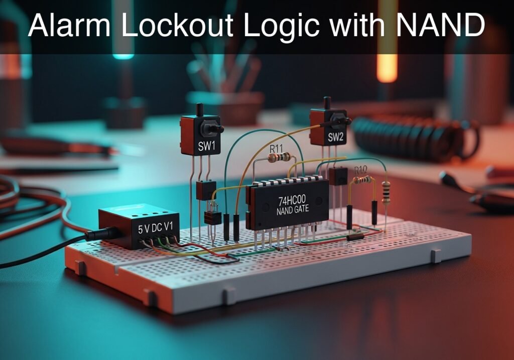
Alarm Lockout Logic with NAND prototype (Maker Style)

Level: Basic – Build an active-high alarm indicator using 74HC00 NAND gates to understand universal logic and signal inversion.

Objective and use case

You will build a digital logic circuit where an alarm sensor and an enable switch must both be triggered to turn on a warning LED, implemented entirely with a single 74HC00 NAND gate chip.

This circuit is highly useful for demonstrating fundamental digital concepts:
* It demonstrates the concept of «universal gates,» showing how a NAND gate can be wired as a NOT gate (inverter) to achieve an AND logic function.
* It illustrates how an «enable» signal works, which is an industry standard method to authorize or safely block system operations.
* It provides hands-on practice with handling CMOS logic levels and configuring pull-down networks for reliable switch operation.

Expected outcome:
* The intermediate signal (the output of the first NAND gate) will output a logic LOW (0 V) only when both inputs are HIGH (5 V).
* The final output will be logic HIGH (5 V) and will light the LED strictly when both the Alarm and Enable inputs are HIGH.
* You will practically verify the combined truth table of a NAND and a NOT gate.

Target audience: Beginners in digital electronics learning how to manipulate logic gates.

Materials

  • V1: 5 V DC supply
  • SW1: SPST switch, function: Alarm trigger
  • SW2: SPST switch, function: Enable signal
  • R1: 10 kΩ resistor, function: pull-down for ALARM node
  • R2: 10 kΩ resistor, function: pull-down for ENABLE node
  • R3: 330 Ω resistor, function: LED current limiting
  • U1: 74HC00 Quad 2-Input NAND Gate, function: logic evaluation and inversion
  • D1: Red LED, function: Alarm indicator

Pin-out of the IC used

74HC00 (Quad 2-Input NAND Gate)

Pin Name Logic function Connection in this case
1 1 A Input 1 of NAND A Node ALARM (from SW1)
2 1B Input 2 of NAND A Node ENABLE (from SW2)
3 1Y Output of NAND A Node INTERMEDIATE
4 2 A Input 1 of NAND B Node INTERMEDIATE
5 2B Input 2 of NAND B Node INTERMEDIATE
6 2Y Output of NAND B Node VOUT
7 GND Ground Node 0
14 VCC Supply Voltage Node VCC

(Note: The 74HC00 contains four independent NAND gates. In this circuit, we use gates A and B. Unused inputs on gates C and D should be tied to ground).

Wiring guide

  • V1: connects between VCC and 0.
  • SW1: connects between VCC and ALARM.
  • R1: connects between ALARM and 0.
  • SW2: connects between VCC and ENABLE.
  • R2: connects between ENABLE and 0.
  • U1 Pin 14 (VCC): connects to VCC.
  • U1 Pin 7 (GND): connects to 0.
  • U1 Pin 1 (1 A): connects to ALARM.
  • U1 Pin 2 (1B): connects to ENABLE.
  • U1 Pin 3 (1Y): connects to INTERMEDIATE.
  • U1 Pin 4 (2 A): connects to INTERMEDIATE.
  • U1 Pin 5 (2B): connects to INTERMEDIATE.
  • U1 Pin 6 (2Y): connects to VOUT.
  • D1: Anode connects to VOUT, Cathode connects to NODE_LED.
  • R3: connects between NODE_LED and 0.
  • Safety connection: Connect pins 9, 10, 12, and 13 of U1 to 0 (GND) to prevent unused gates from floating.

Conceptual block diagram
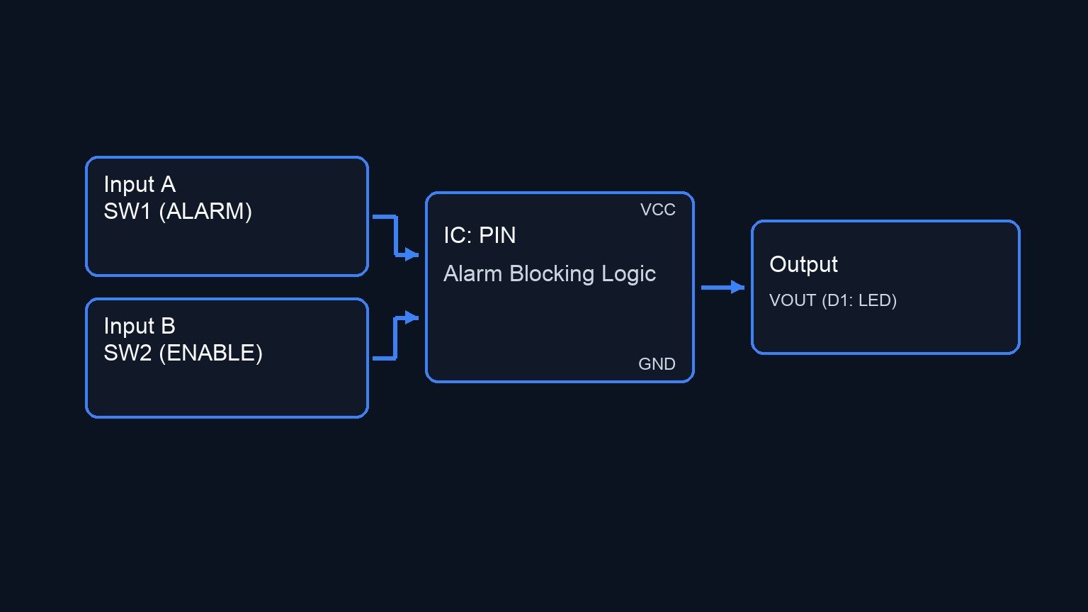
Conceptual block diagram — PIN Alarm Blocking Logic
Quick read: inputs → main block → output (actuator or measurement). This summarizes the ASCII schematic below.

Schematic

VCC --> [ SW1 ] --(ALARM)--> [ U1: Pin 1 (1 A) ]
           |                      |
         [ R1 ]                   |
           |                 [ U1: Gate 1 (NAND) ] --(INTERMEDIATE)--> [ U1: Pins 4,5 (2 A,2B) ]
          GND                     |                                         |
                                  |                                    [ U1: Gate 2 (NAND) ] --(VOUT)--> [ D1: LED ] --(NODE_LED)--> [ R3 ] --> GND
VCC --> [ SW2 ] --(ENABLE)-> [ U1: Pin 2 (1B) ]
           |
         [ R2 ]
           |
          GND

* Power & Safety Connections:
VCC --> [ U1: Pin 14 (VCC) ]
GND <-- [ U1: Pin 7 (GND) ]
GND <-- [ U1: Pins 9, 10, 12, 13 (Unused) ]
Electrical Schematic

Truth table

Alarm (SW1) Enable (SW2) Intermediate Node (1Y) Output Node (2Y) LED State
0 0 1 0 OFF
0 1 1 0 OFF
1 0 1 0 OFF
1 1 0 1 ON

Measurements and tests

  1. Use a multimeter to verify the power supply is exactly 5 V across the VCC and 0 nodes.
  2. Probe the ALARM and ENABLE nodes relative to 0. Verify they read exactly 0 V when their respective switches are open, and 5 V when closed.
  3. Probe the INTERMEDIATE node. It should read ~5 V when either or both switches are open, and drop to ~0 V strictly when both switches are closed.
  4. Probe the VOUT node. It should always display the exact opposite logic level of the INTERMEDIATE node.
  5. Visually confirm that the LED turns on if and only if both switches are toggled to the closed (active) position.

SPICE netlist and simulation

Reference SPICE Netlist (ngspice) — excerptFull SPICE netlist (ngspice)

* Alarm Lockout Logic with NAND

* Main DC Supply
V1 VCC 0 DC 5

* Control signals to simulate user pressing the switches (Testing Truth Table)
V_ctrl1 ctrl1 0 PULSE(0 5 0 1u 1u 50u 100u)
V_ctrl2 ctrl2 0 PULSE(0 5 0 1u 1u 100u 200u)

* SW1: SPST switch (Alarm trigger)
S1 VCC ALARM ctrl1 0 SW_MODEL

* SW2: SPST switch (Enable signal)
S2 VCC ENABLE ctrl2 0 SW_MODEL
.model SW_MODEL SW(VT=2.5 VH=0.5 RON=0.1 ROFF=100MEG)

* Pull-down resistors for logic inputs
R1 ALARM 0 10k
R2 ENABLE 0 10k

* ... (truncated in public view) ...

Copy this content into a .cir file and run with ngspice.

* Alarm Lockout Logic with NAND

* Main DC Supply
V1 VCC 0 DC 5

* Control signals to simulate user pressing the switches (Testing Truth Table)
V_ctrl1 ctrl1 0 PULSE(0 5 0 1u 1u 50u 100u)
V_ctrl2 ctrl2 0 PULSE(0 5 0 1u 1u 100u 200u)

* SW1: SPST switch (Alarm trigger)
S1 VCC ALARM ctrl1 0 SW_MODEL

* SW2: SPST switch (Enable signal)
S2 VCC ENABLE ctrl2 0 SW_MODEL
.model SW_MODEL SW(VT=2.5 VH=0.5 RON=0.1 ROFF=100MEG)

* Pull-down resistors for logic inputs
R1 ALARM 0 10k
R2 ENABLE 0 10k

* U1: 74HC00 Quad 2-Input NAND Gate
* Pinout: 1:1A, 2:1B, 3:1Y, 4:2A, 5:2B, 6:2Y, 7:GND, 8:3Y, 9:3A, 10:3B, 11:4Y, 12:4A, 13:4B, 14:VCC
XU1 ALARM ENABLE INTERMEDIATE INTERMEDIATE INTERMEDIATE VOUT 0 NC8 0 0 NC11 0 0 VCC HC00_DIP14

* D1: Red LED (Alarm indicator)
D1 VOUT NODE_LED DLED
.model DLED D(IS=1e-20 N=2.2 RS=15)

* R3: LED current limiting resistor
R3 NODE_LED 0 330

* Subcircuit for 74HC00 (Quad 2-Input NAND Gate)
.subckt HC00_DIP14 1 2 3 4 5 6 7 8 9 10 11 12 13 14
* Gate 1
B1 3_int 7 V=V(14)*(1-(1/(1+exp(-50*(V(1)-2.5))))*(1/(1+exp(-50*(V(2)-2.5)))))
R1 3_int 3 50
* Gate 2
B2 6_int 7 V=V(14)*(1-(1/(1+exp(-50*(V(4)-2.5))))*(1/(1+exp(-50*(V(5)-2.5)))))
R2 6_int 6 50
* Gate 3
B3 8_int 7 V=V(14)*(1-(1/(1+exp(-50*(V(9)-2.5))))*(1/(1+exp(-50*(V(10)-2.5)))))
R3 8_int 8 50
* Gate 4
B4 11_int 7 V=V(14)*(1-(1/(1+exp(-50*(V(12)-2.5))))*(1/(1+exp(-50*(V(13)-2.5)))))
R4 11_int 11 50
.ends

* Analysis directives
.tran 1u 500u
.print tran V(ALARM) V(ENABLE) V(VOUT) V(NODE_LED)
.op
.end

Simulation Results (Transient Analysis)

Simulation Results (Transient Analysis)
Analysis: The transient simulation shows the output node (VOUT) and LED node (NODE_LED) going high (approx 4.66V and 2.22V respectively) only when both ALARM and ENABLE inputs are high (approx 5V). When either or both inputs are low, the output is near 0V. This matches the intended AND logic behavior created by using two NAND gates in series.
Show raw data table (691 rows)
Index   time            v(alarm)        v(enable)       v(vout)         v(node_led)
0	0.000000e+00	4.999500e-04	4.999500e-04	1.047185e-47	-6.91142e-47
1	1.000000e-08	4.999500e-04	4.999500e-04	7.268458e-64	-4.79767e-63
2	2.000000e-08	4.999500e-04	4.999500e-04	-7.26994e-64	4.797672e-63
3	4.000000e-08	4.999500e-04	4.999500e-04	-7.41841e-68	-2.28156e-77
4	8.000000e-08	4.999500e-04	4.999500e-04	-7.41841e-68	-2.51468e-77
5	1.600000e-07	4.999500e-04	4.999500e-04	-7.41841e-68	-2.44808e-77
6	3.200000e-07	4.999500e-04	4.999500e-04	-7.41841e-68	-2.44808e-77
7	3.750000e-07	4.999500e-04	4.999500e-04	-7.41841e-68	-2.44808e-77
8	4.712500e-07	4.999500e-04	4.999500e-04	-7.41841e-68	-2.44808e-77
9	4.978906e-07	4.999500e-04	4.999500e-04	-7.41841e-68	-2.44808e-77
10	5.445117e-07	4.999500e-04	4.999500e-04	-7.41841e-68	-2.44808e-77
11	5.574158e-07	4.999500e-04	4.999500e-04	-7.41841e-68	-2.44808e-77
12	5.799979e-07	4.999500e-04	4.999500e-04	-7.41841e-68	-2.44808e-77
13	6.049995e-07	4.999950e+00	4.999950e+00	4.662865e+00	2.225088e+00
14	6.550027e-07	4.999950e+00	4.999950e+00	4.662939e+00	2.224602e+00
15	7.550091e-07	4.999950e+00	4.999950e+00	4.662792e+00	2.225571e+00
16	9.550219e-07	4.999950e+00	4.999950e+00	4.662792e+00	2.225574e+00
17	1.000000e-06	4.999950e+00	4.999950e+00	4.662786e+00	2.225611e+00
18	1.040003e-06	4.999950e+00	4.999950e+00	4.662786e+00	2.225611e+00
19	1.120008e-06	4.999950e+00	4.999950e+00	4.662786e+00	2.225611e+00
20	1.280018e-06	4.999950e+00	4.999950e+00	4.662786e+00	2.225611e+00
21	1.600038e-06	4.999950e+00	4.999950e+00	4.662786e+00	2.225611e+00
22	2.240079e-06	4.999950e+00	4.999950e+00	4.662786e+00	2.225611e+00
23	3.240079e-06	4.999950e+00	4.999950e+00	4.662786e+00	2.225611e+00
... (667 more rows) ...


Reference SPICE netlist (ngspice)

* Alarm Lockout Logic with NAND

* Main DC Supply
V1 VCC 0 DC 5

* Control signals to simulate user pressing the switches (Testing Truth Table)
V_ctrl1 ctrl1 0 PULSE(0 5 0 1u 1u 50u 100u)
V_ctrl2 ctrl2 0 PULSE(0 5 0 1u 1u 100u 200u)

* SW1: SPST switch (Alarm trigger)
S1 VCC ALARM ctrl1 0 SW_MODEL

* SW2: SPST switch (Enable signal)
S2 VCC ENABLE ctrl2 0 SW_MODEL
.model SW_MODEL SW(VT=2.5 VH=0.5 RON=0.1 ROFF=100MEG)

* Pull-down resistors for logic inputs
R1 ALARM 0 10k
R2 ENABLE 0 10k

* U1: 74HC00 Quad 2-Input NAND Gate
* Pinout: 1:1A, 2:1B, 3:1Y, 4:2A, 5:2B, 6:2Y, 7:GND, 8:3Y, 9:3A, 10:3B, 11:4Y, 12:4A, 13:4B, 14:VCC
XU1 ALARM ENABLE INTERMEDIATE INTERMEDIATE INTERMEDIATE VOUT 0 NC8 0 0 NC11 0 0 VCC HC00_DIP14

* D1: Red LED (Alarm indicator)
D1 VOUT NODE_LED DLED
.model DLED D(IS=1e-20 N=2.2 RS=15)

* R3: LED current limiting resistor
R3 NODE_LED 0 330

* Subcircuit for 74HC00 (Quad 2-Input NAND Gate)
.subckt HC00_DIP14 1 2 3 4 5 6 7 8 9 10 11 12 13 14
* Gate 1
B1 3_int 7 V=V(14)*(1-(1/(1+exp(-50*(V(1)-2.5))))*(1/(1+exp(-50*(V(2)-2.5)))))
R1 3_int 3 50
* Gate 2
B2 6_int 7 V=V(14)*(1-(1/(1+exp(-50*(V(4)-2.5))))*(1/(1+exp(-50*(V(5)-2.5)))))
R2 6_int 6 50
* Gate 3
B3 8_int 7 V=V(14)*(1-(1/(1+exp(-50*(V(9)-2.5))))*(1/(1+exp(-50*(V(10)-2.5)))))
R3 8_int 8 50
* Gate 4
B4 11_int 7 V=V(14)*(1-(1/(1+exp(-50*(V(12)-2.5))))*(1/(1+exp(-50*(V(13)-2.5)))))
R4 11_int 11 50
.ends

* Analysis directives
.tran 1u 500u
.print tran V(ALARM) V(ENABLE) V(VOUT) V(NODE_LED)
.op
.end

Simulation Results (Transient Analysis)

Simulation Results (Transient Analysis)
Analysis: The transient simulation shows the output node (VOUT) and LED node (NODE_LED) going high (approx 4.66V and 2.22V respectively) only when both ALARM and ENABLE inputs are high (approx 5V). When either or both inputs are low, the output is near 0V. This matches the intended AND logic behavior created by using two NAND gates in series.

Common mistakes and how to avoid them

  1. Leaving unused inputs floating: CMOS chips like the 74HC00 are highly sensitive to static and ambient noise. Unused gate inputs (pins 9, 10, 12, 13) must be explicitly tied to ground (0) or VCC.
  2. Omitting the pull-down resistors: Without R1 and R2, the input pins will float when the switches are open, leading to unpredictable, flickering behavior in the LED. Always ensure the 10 kΩ pull-downs are securely connected to ground.
  3. Connecting the LED without a series resistor: Connecting D1 directly between VOUT and 0 will draw excessive current, potentially destroying the LED and burning out the output stage of the 74HC00 chip. R3 is mandatory.


Troubleshooting

  • Symptom: The LED never turns off, regardless of switch positions.
  • Cause: One of the input pull-down resistors is loose, causing the chip to read a false HIGH, or the intermediate node isn’t wired correctly to both inputs of the second gate.
  • Fix: Verify connections for R1 and R2 to ground. Ensure U1 Pin 3 routes precisely to both Pin 4 and Pin 5.
  • Symptom: The LED brightness flickers when a hand is moved near the circuit.
  • Cause: A floating input is acting as an antenna and picking up environmental noise.
  • Fix: Check that all unused inputs on the IC are tied to ground, and ensure R1 and R2 are seated firmly in the breadboard.
  • Symptom: The IC becomes hot to the touch.
  • Cause: The power supply is connected backwards, or the output node is shorted directly to ground or VCC.
  • Fix: Disconnect power immediately. Verify that U1 Pin 14 goes strictly to +5 V and Pin 7 goes strictly to Ground.

Possible improvements and extensions

  1. Master Override switch: Introduce a third switch and utilize one of the spare NAND gates (e.g., Gate C) to create a «Master Override» that forces the LED off regardless of the Alarm and Enable signals.
  2. Add a delay circuit: Incorporate an RC network (a resistor and a capacitor) between one of the switches and its input pin. This requires the switch to be held closed for a specific duration before the logic gate registers a HIGH signal, preventing false alarms.

More Practical Cases on Prometeo.blog

Find this product and/or books on this topic on Amazon

Go to Amazon

As an Amazon Associate, I earn from qualifying purchases. If you buy through this link, you help keep this project running.

Quick Quiz

Question 1: What is the main objective of the circuit described in the article?


Question 2: Which logic gate chip is used exclusively in this project?


Question 3: How is the AND logic function achieved in this circuit using only NAND gates?


Question 4: What is the purpose of the 'enable' signal in this system?


Question 5: What is the expected voltage of the intermediate signal (output of the first NAND gate) when both inputs are HIGH?


Question 6: Under what condition will the final output light the warning LED?


Question 7: Why are pull-down networks used in this circuit?


Question 8: What logic family's levels does this project provide hands-on practice with?


Question 9: What combined truth table will you practically verify in this project?


Question 10: What is the difficulty level of this project?


Carlos Núñez Zorrilla
Electronics & Computer Engineer

Telecommunications Electronics Engineer and Computer Engineer (official degrees in Spain).
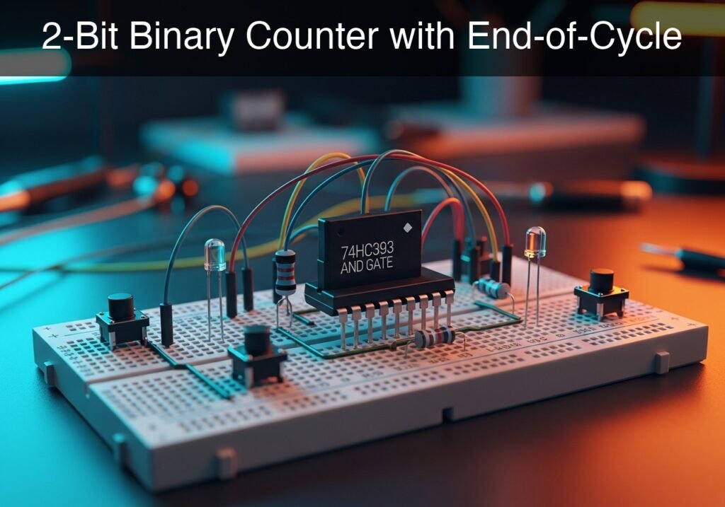
Follow me:


Practical case: 2-Bit Binary Counter with End-of-Cycle

2-Bit Binary Counter with End-of-Cycle prototype (Maker Style)

Level: Basic – Build a 0 to 3 binary counter with manual clock, reset, and a maximum count indicator.

Objective and use case

In this practical case, you will build a 2-bit digital counter using a 74HC393 IC and decode its maximum state (binary 11, decimal 3) using a 74HC08 AND gate. A simulated clock pushbutton increments the count, while a manual reset pushbutton forces the counter back to zero.

Why this is useful:
* Demonstrates how sequential logic (counters) tracks discrete events over time.
* Shows how combinational logic (AND gate) is used to decode specific binary states and trigger events.
* Provides a foundational understanding of clock edge triggering and asynchronous resets.
* Acts as a building block for state machines, timers, and step-sequencers in industrial or hobbyist electronics.

Expected outcome:
* Pressing and releasing the clock button will advance the binary state sequentially: 00 → 01 → 10 → 11.
* Two LEDs will display the current binary count (LSB and MSB).
* A third LED (end-of-cycle indicator) will light up strictly when the count reaches state 3.
* Pressing the reset button will immediately extinguish all LEDs, returning the circuit to state 00 regardless of the current count.
* Target audience: Electronics beginners learning digital logic and basic state tracking.

Materials

  • V1: 5 V DC supply
  • S1: normally open pushbutton, function: clock pulse generator
  • S2: normally open pushbutton, function: manual reset trigger
  • R1: 10 kΩ resistor, function: pull-down for CLK node
  • R2: 10 kΩ resistor, function: pull-down for MR node
  • R3: 330 Ω resistor, function: current limiting for QA LED
  • R4: 330 Ω resistor, function: current limiting for QB LED
  • R5: 330 Ω resistor, function: current limiting for MAX_VAL LED
  • D1: green LED, function: LSB indicator (QA)
  • D2: yellow LED, function: MSB indicator (QB)
  • D3: red LED, function: end-of-cycle indicator
  • U1: 74HC393 dual 4-bit binary counter, function: state counting
  • U2: 74HC08 quad 2-input AND gate, function: state decoding

Pin-out of the IC used

74HC393 (Dual 4-Bit Binary Counter – Only Half Used)

Pin Name Logic function Connection in this case
1 1CP Clock Input (Active Low / Falling Edge) CLK
2 1MR Master Reset (Active High) MR
3 1Q0 Output 0 (LSB) QA
4 1Q1 Output 1 (MSB) QB
7 GND Ground 0
14 VCC Positive Supply VCC

Note: Pins 5, 6, and 8 through 13 belong to the second counter and can be grounded in a real circuit to prevent floating inputs.

74HC08 (Quad 2-Input AND Gate – Only One Gate Used)

Pin Name Logic function Connection in this case
1 1 A Input A of Gate 1 QA
2 1B Input B of Gate 1 QB
3 1Y Output of Gate 1 MAX_VAL
7 GND Ground 0
14 VCC Positive Supply VCC

Wiring guide

  • V1: connects between VCC and 0.
  • S1: connects between VCC and CLK.
  • R1: connects between CLK and 0.
  • S2: connects between VCC and MR.
  • R2: connects between MR and 0.
  • U1: Pin 1 connects to CLK, Pin 2 connects to MR, Pin 3 connects to QA, Pin 4 connects to QB, Pin 7 connects to 0, Pin 14 connects to VCC.
  • U2: Pin 1 connects to QA, Pin 2 connects to QB, Pin 3 connects to MAX_VAL, Pin 7 connects to 0, Pin 14 connects to VCC.
  • R3: connects between QA and N_D1.
  • D1: connects between N_D1 and 0 (anode to N_D1, cathode to 0).
  • R4: connects between QB and N_D2.
  • D2: connects between N_D2 and 0 (anode to N_D2, cathode to 0).
  • R5: connects between MAX_VAL and N_D3.
  • D3: connects between N_D3 and 0 (anode to N_D3, cathode to 0).

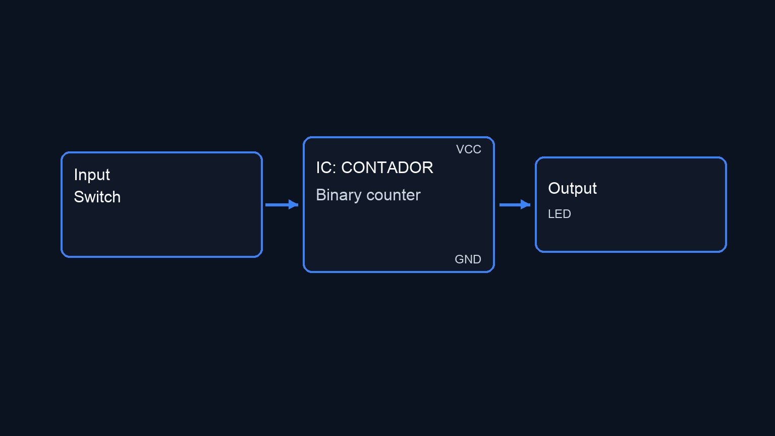
Conceptual block diagram

Conceptual block diagram — CONTADOR Binary counter
Quick read: inputs → main block → output (actuator or measurement). This summarizes the ASCII schematic below.

Schematic

[ S1 (Clock) + R1 ] --(CLK)--> [                       ] --(QA)--> [ R3 (330 Ω) ] --> [ D1 (Green LED) ] ---> GND
                               [                       ]
                               [                       ] --(QA)--> [                       ]
                               [ U1: 74HC393 Counter   ]           [ U2: 74HC08 AND Gate   ] --(MAX_VAL)--> [ R5 (330 Ω) ] --> [ D3 (Red LED) ] ---> GND
                               [                       ] --(QB)--> [                       ]
                               [                       ]
[ S2 (Reset) + R2 ] --(MR)---> [                       ] --(QB)--> [ R4 (330 Ω) ] --> [ D2 (Yellow LED) ] --> GND
Electrical Schematic

Measurements and tests

  1. Initial State Check: Power on the circuit. If any LEDs are lit, press and release S2 (Master Reset). The voltage at the MR node will spike to 5 V, clearing the counter. Measure QA, QB, and MAX_VAL; all should be 0 V. All LEDs must be OFF.
  2. First Clock Pulse (State 1): Press and hold S1. The CLK node goes to 5 V. Release S1. The 74HC393 triggers on the falling edge (high-to-low transition). D1 (QA) should turn on. D2 (QB) and D3 (MAX_VAL) remain off.
  3. Second Clock Pulse (State 2): Press and release S1 again. D1 turns off and D2 turns on. This represents binary 10 (decimal 2).
  4. Third Clock Pulse (State 3): Press and release S1 a third time. Both D1 (QA) and D2 (QB) turn on. Consequently, inputs 1 A and 1B on the 74HC08 are both HIGH. The MAX_VAL node will output 5 V, lighting up the end-of-cycle LED (D3).
  5. Rollover (State 0): Press and release S1 a fourth time. The counter overflows the 2-bit capacity represented by QA and QB. Both counting LEDs and the MAX_VAL LED will turn off.
  6. Asynchronous Reset Verification: Cycle the counter to state 2 or 3. Press the reset button S2. Observe that the counter immediately resets to 00 without waiting for a clock pulse.

SPICE netlist and simulation

Reference SPICE Netlist (ngspice) — excerptFull SPICE netlist (ngspice)

* Practical case: 2-Bit Binary Counter with End-of-Cycle

.width out=256

* --- Power Supply ---
V1 VCC 0 DC 5

* --- User Inputs (Pushbuttons modeled as Voltage-Controlled Switches) ---
* Clock Pushbutton (S1) connects VCC to CLK
S1 VCC CLK S1_ctrl 0 mySW
Vctrl1 S1_ctrl 0 PULSE(0 5 20u 1u 1u 40u 100u)
R1 CLK 0 10k

* Manual Reset Pushbutton (S2) connects VCC to MR
S2 VCC MR S2_ctrl 0 mySW
* Initialize reset at start, then trigger again at 280us to clear the MAX_VAL state
Vctrl2 S2_ctrl 0 PWL(0 5 10u 5 11u 0 280u 0 281u 5 290u 5 291u 0)
R2 MR 0 10k

.model mySW SW(Ron=1 Roff=100Meg Vt=2.5 Vh=0.5)
* ... (truncated in public view) ...

Copy this content into a .cir file and run with ngspice.

* Practical case: 2-Bit Binary Counter with End-of-Cycle

.width out=256

* --- Power Supply ---
V1 VCC 0 DC 5

* --- User Inputs (Pushbuttons modeled as Voltage-Controlled Switches) ---
* Clock Pushbutton (S1) connects VCC to CLK
S1 VCC CLK S1_ctrl 0 mySW
Vctrl1 S1_ctrl 0 PULSE(0 5 20u 1u 1u 40u 100u)
R1 CLK 0 10k

* Manual Reset Pushbutton (S2) connects VCC to MR
S2 VCC MR S2_ctrl 0 mySW
* Initialize reset at start, then trigger again at 280us to clear the MAX_VAL state
Vctrl2 S2_ctrl 0 PWL(0 5 10u 5 11u 0 280u 0 281u 5 290u 5 291u 0)
R2 MR 0 10k

.model mySW SW(Ron=1 Roff=100Meg Vt=2.5 Vh=0.5)
.model logic_sw SW(Ron=1k Roff=100Meg Vt=2.5 Vh=0.1)

* --- Subcircuits for Logic ---

* Falling-edge triggered T-Flip-Flop with active-high asynchronous reset
.subckt TFF_falling CLK CLR Q
B1 CLK_b 0 V=5-V(CLK)
S1 Q_b master CLK 0 logic_sw
C1 master 0 100p
R1 master 0 1G
S2 master slave CLK_b 0 logic_sw
C2 slave 0 100p
R2 slave 0 1G
* Asynchronous Reset Switches
S3 master 0 CLR 0 logic_sw
S4 slave 0 CLR 0 logic_sw
* Output formatting with RC filter to prevent timestep discontinuities
B2 Q_raw 0 V=V(slave)>2.5?5:0
R3 Q_raw Q 1k
C3 Q 0 100p
B4 Q_b 0 V=5-V(Q_raw)
.ends

* U1: 74HC393 Dual 4-bit Binary Counter (Only first 2 bits QA, QB modeled)
.subckt 74HC393 CLK MR QA QB GND VCC
X1 CLK MR QA TFF_falling
X2 QA MR QB TFF_falling
.ends

* U2: 74HC08 Quad 2-input AND Gate
.subckt 74HC08 A B Y GND VCC
B1 Y_raw 0 V=(V(A)>2.5)&&(V(B)>2.5)?5:0
R1 Y_raw Y 1k
C1 Y 0 100p
.ends

* --- Main Circuit ---

* U1: 74HC393 Dual 4-bit Binary Counter
XU1 CLK MR QA QB 0 VCC 74HC393

* U2: 74HC08 Quad 2-input AND gate
XU2 QA QB MAX_VAL 0 VCC 74HC08

* --- Output LEDs ---
R3 QA N_D1 330
D1 N_D1 0 LED_green

R4 QB N_D2 330
D2 N_D2 0 LED_yellow

R5 MAX_VAL N_D3 330
D3 N_D3 0 LED_red

.model LED_green D(IS=1e-19 N=1.8 RS=10)
.model LED_yellow D(IS=1e-19 N=1.7 RS=10)
.model LED_red D(IS=1e-19 N=1.6 RS=10)

* --- Simulation and Output ---
.op
.tran 1u 600u
.print tran V(CLK) V(MR) V(QA) V(QB) V(MAX_VAL)
.end

Simulation Results (Transient Analysis)

Simulation Results (Transient Analysis)
Analysis: The simulation shows the clock signal toggling and the manual reset (MR) signal initializing high then pulsing later. The QA output toggles in response to the clock, but QB and MAX_VAL remain near zero throughout the sampled data, indicating the counter may not be fully reaching the higher states or the clock pulses are insufficient to trigger QB.
Show raw data table (1035 rows)
Index   time            v(clk)          v(mr)           v(qa)           v(qb)           v(max_val)
0	0.000000e+00	4.999500e-04	4.999500e+00	1.094960e-64	1.402927e-64	1.824146e-64
1	1.000000e-08	4.999500e-04	4.999500e+00	9.954179e-65	1.275388e-64	1.658315e-64
2	2.000000e-08	4.999500e-04	4.999500e+00	9.049254e-65	1.159444e-64	1.507559e-64
3	4.000000e-08	4.999500e-04	4.999500e+00	7.403935e-65	9.486357e-65	1.233457e-64
4	8.000000e-08	4.999500e-04	4.999500e+00	4.935957e-65	6.324238e-65	8.223048e-65
5	1.600000e-07	4.999500e-04	4.999500e+00	2.115410e-65	2.710388e-65	3.524164e-65
6	3.200000e-07	4.999500e-04	4.999500e+00	2.350456e-66	3.011542e-66	3.915737e-66
7	6.400000e-07	4.999500e-04	4.999500e+00	-5.42413e-67	-6.94971e-67	-9.03632e-67
8	1.280000e-06	4.999500e-04	4.999500e+00	2.841210e-67	3.640325e-67	4.733309e-67
9	2.280000e-06	4.999500e-04	4.999500e+00	-1.89414e-67	-2.42688e-67	-3.15554e-67
10	3.280000e-06	4.999500e-04	4.999500e+00	1.262760e-67	1.617922e-67	2.103693e-67
11	4.280000e-06	4.999500e-04	4.999500e+00	-8.41840e-68	-1.07861e-67	-1.40246e-67
12	5.280000e-06	4.999500e-04	4.999500e+00	5.612267e-68	7.190766e-68	9.349746e-68
13	6.280000e-06	4.999500e-04	4.999500e+00	-3.74151e-68	-4.79384e-68	-6.23316e-68
14	7.280000e-06	4.999500e-04	4.999500e+00	2.494341e-68	3.195896e-68	4.155443e-68
15	8.280000e-06	4.999500e-04	4.999500e+00	-1.66289e-68	-2.13060e-68	-2.77030e-68
16	9.280000e-06	4.999500e-04	4.999500e+00	1.108596e-68	1.420398e-68	1.846863e-68
17	1.000000e-05	4.999500e-04	4.999500e+00	-6.26598e-69	-8.02834e-69	-1.04388e-68
18	1.010000e-05	4.999500e-04	4.999500e+00	-3.13299e-69	-4.01417e-69	-5.21940e-69
19	1.030000e-05	4.999500e-04	4.999500e+00	1.566513e-78	2.007109e-78	2.609729e-78
20	1.035875e-05	4.999500e-04	4.999500e+00	8.551514e-79	1.095671e-78	1.424639e-78
21	1.046156e-05	4.999500e-04	4.999500e+00	2.744610e-79	3.516558e-79	4.572383e-79
22	1.049002e-05	4.999500e-04	4.999500e+00	2.060863e-79	2.640500e-79	3.433294e-79
23	1.053982e-05	4.999500e-04	4.999500e+00	1.239160e-79	1.587686e-79	2.064379e-79
... (1011 more rows) ...


Reference SPICE netlist (ngspice)

* Practical case: 2-Bit Binary Counter with End-of-Cycle

.width out=256

* --- Power Supply ---
V1 VCC 0 DC 5

* --- User Inputs (Pushbuttons modeled as Voltage-Controlled Switches) ---
* Clock Pushbutton (S1) connects VCC to CLK
S1 VCC CLK S1_ctrl 0 mySW
Vctrl1 S1_ctrl 0 PULSE(0 5 20u 1u 1u 40u 100u)
R1 CLK 0 10k

* Manual Reset Pushbutton (S2) connects VCC to MR
S2 VCC MR S2_ctrl 0 mySW
* Initialize reset at start, then trigger again at 280us to clear the MAX_VAL state
Vctrl2 S2_ctrl 0 PWL(0 5 10u 5 11u 0 280u 0 281u 5 290u 5 291u 0)
R2 MR 0 10k

.model mySW SW(Ron=1 Roff=100Meg Vt=2.5 Vh=0.5)
.model logic_sw SW(Ron=1k Roff=100Meg Vt=2.5 Vh=0.1)

* --- Subcircuits for Logic ---

* Falling-edge triggered T-Flip-Flop with active-high asynchronous reset
.subckt TFF_falling CLK CLR Q
B1 CLK_b 0 V=5-V(CLK)
S1 Q_b master CLK 0 logic_sw
C1 master 0 100p
R1 master 0 1G
S2 master slave CLK_b 0 logic_sw
C2 slave 0 100p
R2 slave 0 1G
* Asynchronous Reset Switches
S3 master 0 CLR 0 logic_sw
S4 slave 0 CLR 0 logic_sw
* Output formatting with RC filter to prevent timestep discontinuities
B2 Q_raw 0 V=V(slave)>2.5?5:0
R3 Q_raw Q 1k
C3 Q 0 100p
B4 Q_b 0 V=5-V(Q_raw)
.ends

* U1: 74HC393 Dual 4-bit Binary Counter (Only first 2 bits QA, QB modeled)
.subckt 74HC393 CLK MR QA QB GND VCC
X1 CLK MR QA TFF_falling
X2 QA MR QB TFF_falling
.ends

* U2: 74HC08 Quad 2-input AND Gate
.subckt 74HC08 A B Y GND VCC
B1 Y_raw 0 V=(V(A)>2.5)&&(V(B)>2.5)?5:0
R1 Y_raw Y 1k
C1 Y 0 100p
.ends

* --- Main Circuit ---

* U1: 74HC393 Dual 4-bit Binary Counter
XU1 CLK MR QA QB 0 VCC 74HC393

* U2: 74HC08 Quad 2-input AND gate
XU2 QA QB MAX_VAL 0 VCC 74HC08

* --- Output LEDs ---
R3 QA N_D1 330
D1 N_D1 0 LED_green

R4 QB N_D2 330
D2 N_D2 0 LED_yellow

R5 MAX_VAL N_D3 330
D3 N_D3 0 LED_red

.model LED_green D(IS=1e-19 N=1.8 RS=10)
.model LED_yellow D(IS=1e-19 N=1.7 RS=10)
.model LED_red D(IS=1e-19 N=1.6 RS=10)

* --- Simulation and Output ---
.op
.tran 1u 600u
.print tran V(CLK) V(MR) V(QA) V(QB) V(MAX_VAL)
.end

Simulation Results (Transient Analysis)

Simulation Results (Transient Analysis)
Analysis: The simulation shows the clock signal toggling and the manual reset (MR) signal initializing high then pulsing later. The QA output toggles in response to the clock, but QB and MAX_VAL remain near zero throughout the sampled data, indicating the counter may not be fully reaching the higher states or the clock pulses are insufficient to trigger QB.

Common mistakes and how to avoid them

  • Ignoring switch bounce: Mechanical pushbuttons exhibit «bounce,» creating multiple rapid voltage transitions on a single press. This causes the counter to skip numbers. Avoid this in critical applications by using a hardware debounce circuit (like an RC filter followed by a Schmitt trigger).
  • Misunderstanding the clock edge: The 74HC393 increments on the falling edge of the clock signal. Beginners often expect the count to increase the moment the button is pressed, but it actually increases the moment the button is released (when the voltage drops from 5 V to 0 V).
  • Leaving unused logic inputs floating: While this basic test circuit focuses on the used gates, leaving the inputs of the unused gates on the 74HC393 and 74HC08 floating can cause internal oscillation and excessive power draw. Always tie unused inputs to GND or VCC.


Troubleshooting

  • Symptom: The counter jumps randomly (e.g., skips from 0 to 2 or 3).
  • Cause: Mechanical switch bounce on S1 is sending multiple clock pulses instantly.
  • Fix: Add a 100 nF capacitor in parallel with R1 to filter out the rapid mechanical bounces, or press the button very deliberately.
  • Symptom: The counter never increments; LEDs remain off.
  • Cause: The master reset pin is stuck HIGH, keeping the counter constantly cleared.
  • Fix: Check R2. Ensure it is firmly connected to GND to pull the MR node LOW when the reset button is not pressed.
  • Symptom: LEDs D1 and D2 count correctly, but D3 never turns on.
  • Cause: The 74HC08 AND gate is not receiving power, or its inputs are incorrectly wired.
  • Fix: Verify that pins 14 (VCC) and 7 (GND) of U2 are connected. Double-check that pin 1 connects to QA and pin 2 connects to QB.
  • Symptom: LEDs are very dim or burn out instantly.
  • Cause: Incorrect or missing current-limiting resistors.
  • Fix: Ensure R3, R4, and R5 (330 Ω) are properly placed in series with the respective LED anodes.

Possible improvements and extensions

  • Hardware Debouncing with a Schmitt Trigger: Replace the simple S1/R1 clock with an RC network fed into a 74HC14 Schmitt trigger inverter to completely eliminate switch bounce and provide perfectly clean clock edges.
  • Auto-Reset for Modulo-3 Counting: Connect the MAX_VAL output (pin 3 of U2) directly to the Master Reset input (MR, pin 2 of U1) instead of using the manual S2 switch. This will automatically clear the counter the instant it hits state 3, turning it into a 0-to-2 recurring cycle counter.

More Practical Cases on Prometeo.blog

Find this product and/or books on this topic on Amazon

Go to Amazon

As an Amazon Associate, I earn from qualifying purchases. If you buy through this link, you help keep this project running.

Quick Quiz

Question 1: What is the main objective of this practical case?


Question 2: Which integrated circuit (IC) is used as the digital counter in this project?


Question 3: What is the specific purpose of the 74HC08 AND gate in this circuit?


Question 4: What happens when the clock pushbutton is pressed and released?


Question 5: What is the maximum decimal state this counter can reach before it wraps around or is reset?


Question 6: What is the function of the third LED in the circuit?


Question 7: What is the immediate effect of pressing the manual reset pushbutton?


Question 8: According to the text, what does sequential logic (counters) track?


Question 9: Which type of logic is demonstrated by using the AND gate to decode specific binary states?


Question 10: What is one of the applications this circuit acts as a building block for?


Carlos Núñez Zorrilla
Electronics & Computer Engineer

Telecommunications Electronics Engineer and Computer Engineer (official degrees in Spain).
Follow me:


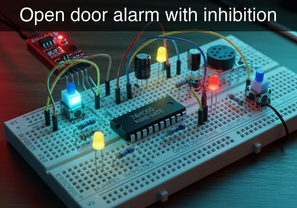
Practical case: Open door alarm with inhibition

Open door alarm with inhibition prototype (Maker Style)

Level: Basic – Design a logic circuit using a 74HC00 NAND gate to trigger an LED alarm only when the door is open and the system is enabled.

Objective and use case

What you will build is a basic security system logic controller using the universal 74HC00 NAND chip. The circuit processes two discrete inputs (a door sensor and an enable switch) to activate a visual alarm strictly when the system is armed and a breach occurs.

Why it is useful:
* It demonstrates how multiple NAND gates can be combined to form an AND logic gate.
* It illustrates the concept of a hardware «enable/inhibit» signal commonly used in industrial and digital electronics.
* It provides practical experience in interfacing mechanical switches with digital CMOS inputs without floating states.

Expected outcome:
* When the door switch is open (Logic 1) AND the enable switch is closed (Logic 1), the LED turns ON.
* If the enable switch is open (Logic 0), the alarm remains inhibited (LED OFF) regardless of the door state.
* Logic High (VCC) and Logic Low (0 V) voltages can be clearly measured at the switch output nodes.
* The intermediate logic signal between the two NAND gates will correctly show the inverted state of the final output.

Target audience and level: Electronics beginners learning digital logic and combinational circuits.

Materials

  • V1: 5 V DC supply, function: main circuit power
  • SW1: SPST switch, function: door sensor (closed = logic 0, open = logic 1)
  • SW2: SPST switch, function: system enable (inhibited = logic 0, armed = logic 1)
  • R1: 10 kΩ resistor, function: pull-down for SW1 at node DOOR
  • R2: 10 kΩ resistor, function: pull-down for SW2 at node EN
  • R3: 330 Ω resistor, function: LED current limiting
  • U1: 74HC00 quad 2-input NAND gate, function: logic processing
  • D1: red LED, function: visual alarm indicator

Pin-out of the IC used

IC used: 74HC00 (Quad 2-Input NAND Gate)

Pin Name Logic function Connection in this case
1 1 A Input A of Gate 1 Node DOOR (from SW1)
2 1B Input B of Gate 1 Node EN (from SW2)
3 1Y Output of Gate 1 Node NAND_OUT
4 2 A Input A of Gate 2 Node NAND_OUT (tied to 2B)
5 2B Input B of Gate 2 Node NAND_OUT (tied to 2 A)
6 2Y Output of Gate 2 Node ALARM
7 GND Ground reference Node 0
14 VCC Positive supply Node VCC

(Note: Unused input pins 9, 10, 12, and 13 should be tied to ground in physical builds to prevent CMOS oscillation.)

Wiring guide

  • V1: connects between VCC (positive) and 0 (GND).
  • SW1: connects between VCC and DOOR.
  • R1: connects between DOOR and 0.
  • SW2: connects between VCC and EN.
  • R2: connects between EN and 0.
  • U1:
  • Pin 1 connects to DOOR.
  • Pin 2 connects to EN.
  • Pin 3 connects to NAND_OUT.
  • Pin 4 connects to NAND_OUT.
  • Pin 5 connects to NAND_OUT.
  • Pin 6 connects to ALARM.
  • Pin 7 connects to 0.
  • Pin 14 connects to VCC.
  • R3: connects between ALARM and LED_IN.
  • D1: anode connects to LED_IN, cathode connects to 0.

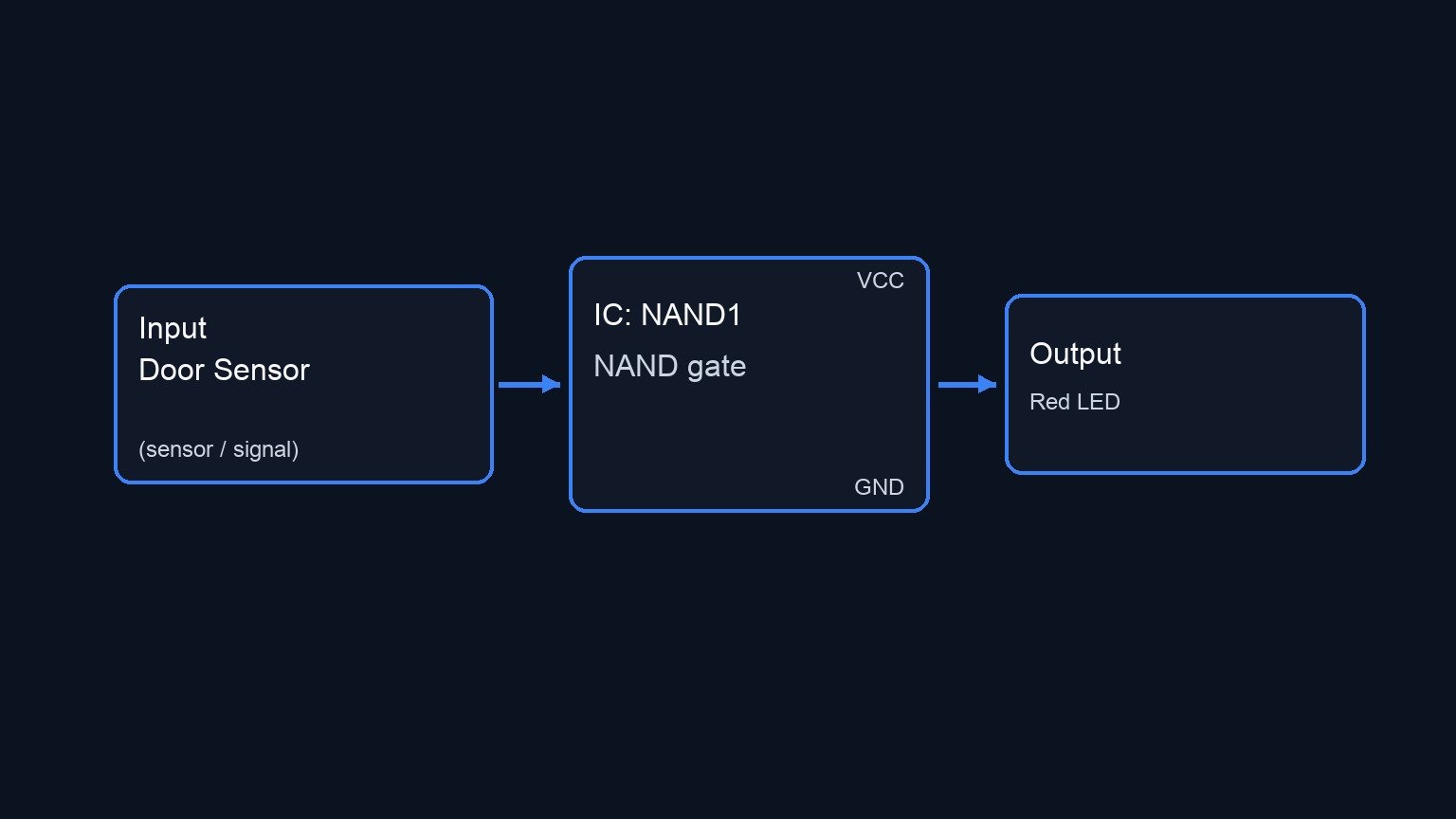
Conceptual block diagram

Conceptual block diagram — NAND1 NAND gate
Quick read: inputs → main block → output (actuator or measurement). This summarizes the ASCII schematic below.

Schematic

VCC --> [ SW1: Door Sensor ] --+--(DOOR)----->+
                               |              |
                         [ R1: 10 kΩ ]         v
                               |        [ U1: NAND1 ] --(NAND_OUT)--> [ U1: NAND2 ] --(ALARM)--> [ R3: 330 Ω ] --(LED_IN)--> [ D1: Red LED ] --> GND
                              GND       [ Pins 1,2->3 ]               [ Pins 4,5->6 ]
                                              ^
                                              |
VCC --> [ SW2: Sys Enable ] ---+--(EN)------->+
                               |
                         [ R2: 10 kΩ ]
                               |
                              GND
Electrical Schematic

Truth table

DOOR (SW1) EN (SW2) NAND_OUT (Pin 3) ALARM (Pin 6) LED Status
0 (Low) 0 (Low) 1 (High) 0 (Low) OFF
0 (Low) 1 (High) 1 (High) 0 (Low) OFF
1 (High) 0 (Low) 1 (High) 0 (Low) OFF
1 (High) 1 (High) 0 (Low) 1 (High) ON (Alarm Active)

Measurements and tests

  1. Supply Validation: Measure the voltage between VCC and 0. Ensure it is a stable 5 V.
  2. Input States: Use a multimeter to measure nodes DOOR and EN with respect to ground (0). Verify they read 0 V when the switch is open and 5 V when the switch is closed.
  3. Intermediate Logic: Close both SW1 and SW2. Measure node NAND_OUT. It should drop to 0 V (Logic Low) only when both switches are closed.
  4. Final Output: Measure node ALARM. It should read 5 V (Logic High) only when both switches are closed, confirming that U1B correctly inverted the signal from U1 A.
  5. Load Check: Verify the voltage drop across D1 is roughly 1.8 V to 2.2 V when illuminated.

SPICE netlist and simulation

Reference SPICE Netlist (ngspice) — excerptFull SPICE netlist (ngspice)

* Practical case: Open door alarm with inhibition
.width out=256

* Main Power Supply
V1 VCC 0 DC 5

* Door Sensor (SW1) - Modeled as a voltage-controlled switch with a pulse source
V_ctrl1 ctrl1 0 PULSE(0 5 0 1u 1u 50u 100u)
S1 VCC DOOR ctrl1 0 mySW
R1 DOOR 0 10k

* System Enable (SW2) - Modeled as a voltage-controlled switch with a slower pulse source
V_ctrl2 ctrl2 0 PULSE(0 5 0 1u 1u 100u 200u)
S2 VCC EN ctrl2 0 mySW
R2 EN 0 10k

* 74HC00 Quad 2-input NAND gate
* Wiring: 1->DOOR, 2->EN, 3->NAND_OUT, 4->NAND_OUT, 5->NAND_OUT, 6->ALARM, 7->0, 14->VCC
XU1 DOOR EN NAND_OUT NAND_OUT NAND_OUT ALARM 0 VCC 74HC00

* ... (truncated in public view) ...

Copy this content into a .cir file and run with ngspice.

* Practical case: Open door alarm with inhibition
.width out=256

* Main Power Supply
V1 VCC 0 DC 5

* Door Sensor (SW1) - Modeled as a voltage-controlled switch with a pulse source
V_ctrl1 ctrl1 0 PULSE(0 5 0 1u 1u 50u 100u)
S1 VCC DOOR ctrl1 0 mySW
R1 DOOR 0 10k

* System Enable (SW2) - Modeled as a voltage-controlled switch with a slower pulse source
V_ctrl2 ctrl2 0 PULSE(0 5 0 1u 1u 100u 200u)
S2 VCC EN ctrl2 0 mySW
R2 EN 0 10k

* 74HC00 Quad 2-input NAND gate
* Wiring: 1->DOOR, 2->EN, 3->NAND_OUT, 4->NAND_OUT, 5->NAND_OUT, 6->ALARM, 7->0, 14->VCC
XU1 DOOR EN NAND_OUT NAND_OUT NAND_OUT ALARM 0 VCC 74HC00

* Alarm LED indicator
R3 ALARM LED_IN 330
D1 LED_IN 0 DLED

* Models and Subcircuits
.model mySW SW(Ron=1 Roff=100Meg Vt=2.5)
.model DLED D(IS=1e-15 N=2 RS=10)

* 74HC00 Subcircuit implementation (using robust continuous B-sources for logic)
.subckt 74HC00 1 2 3 4 5 6 7 14
* Gate 1 (Pins 1, 2 -> 3)
B1 3 7 V = 5 * (1 - (1 / (1 + exp(-50*(V(1,7)-2.5)))) * (1 / (1 + exp(-50*(V(2,7)-2.5)))))
* Gate 2 (Pins 4, 5 -> 6)
B2 6 7 V = 5 * (1 - (1 / (1 + exp(-50*(V(4,7)-2.5)))) * (1 / (1 + exp(-50*(V(5,7)-2.5)))))
* Dummy loads to prevent floating pins
R1 1 7 100Meg
R2 2 7 100Meg
R3 4 7 100Meg
R4 5 7 100Meg
R5 14 7 100Meg
.ends

* Analysis Directives
.op
.tran 1u 300u
.print tran V(DOOR) V(EN) V(ALARM) V(LED_IN)
.end

Simulation Results (Transient Analysis)

Simulation Results (Transient Analysis)
Analysis: The simulation results show that when both DOOR and EN are high (approx 5V), ALARM goes high (5V) and LED_IN reaches about 1.65V, indicating the LED is ON. When either DOOR or EN is low (approx 0V), ALARM is low (0V) and LED_IN is 0V, indicating the LED is OFF. This perfectly matches the intended truth table for the alarm with inhibition.
Show raw data table (412 rows)
Index   time            v(door)         v(en)           v(alarm)        v(led_in)
0	0.000000e+00	4.999000e-04	4.999000e-04	-7.41841e-68	4.091162e-30
1	1.000000e-08	4.999000e-04	4.999000e-04	-7.41841e-68	2.688961e-41
2	2.000000e-08	4.999000e-04	4.999000e-04	-7.41841e-68	-2.68896e-41
3	4.000000e-08	4.999000e-04	4.999000e-04	-7.41841e-68	-8.83675e-52
4	8.000000e-08	4.999000e-04	4.999000e-04	-7.41841e-68	3.534698e-52
5	1.600000e-07	4.999000e-04	4.999000e-04	-7.41841e-68	1.858568e-62
6	3.200000e-07	4.999000e-04	4.999000e-04	-7.41841e-68	-4.64651e-63
7	3.562500e-07	4.999000e-04	4.999000e-04	-7.41841e-68	-7.41842e-68
8	4.196875e-07	4.999000e-04	4.999000e-04	-7.41841e-68	-7.41841e-68
9	4.372461e-07	4.999000e-04	4.999000e-04	-7.41841e-68	-7.41841e-68
10	4.679736e-07	4.999000e-04	4.999000e-04	-7.41841e-68	-7.41841e-68
11	5.019934e-07	4.999500e+00	4.999500e+00	5.000000e+00	1.651140e+00
12	5.700330e-07	4.999500e+00	4.999500e+00	5.000000e+00	1.651062e+00
13	7.061121e-07	4.999500e+00	4.999500e+00	5.000000e+00	1.650721e+00
14	9.782703e-07	4.999500e+00	4.999500e+00	5.000000e+00	1.650725e+00
15	1.000000e-06	4.999500e+00	4.999500e+00	5.000000e+00	1.650721e+00
16	1.043459e-06	4.999500e+00	4.999500e+00	5.000000e+00	1.650721e+00
17	1.130378e-06	4.999500e+00	4.999500e+00	5.000000e+00	1.650721e+00
18	1.304216e-06	4.999500e+00	4.999500e+00	5.000000e+00	1.650721e+00
19	1.651892e-06	4.999500e+00	4.999500e+00	5.000000e+00	1.650721e+00
20	2.347244e-06	4.999500e+00	4.999500e+00	5.000000e+00	1.650721e+00
21	3.347244e-06	4.999500e+00	4.999500e+00	5.000000e+00	1.650721e+00
22	4.347244e-06	4.999500e+00	4.999500e+00	5.000000e+00	1.650721e+00
23	5.347244e-06	4.999500e+00	4.999500e+00	5.000000e+00	1.650721e+00
... (388 more rows) ...


Reference SPICE netlist (ngspice)

* Practical case: Open door alarm with inhibition
.width out=256

* Main Power Supply
V1 VCC 0 DC 5

* Door Sensor (SW1) - Modeled as a voltage-controlled switch with a pulse source
V_ctrl1 ctrl1 0 PULSE(0 5 0 1u 1u 50u 100u)
S1 VCC DOOR ctrl1 0 mySW
R1 DOOR 0 10k

* System Enable (SW2) - Modeled as a voltage-controlled switch with a slower pulse source
V_ctrl2 ctrl2 0 PULSE(0 5 0 1u 1u 100u 200u)
S2 VCC EN ctrl2 0 mySW
R2 EN 0 10k

* 74HC00 Quad 2-input NAND gate
* Wiring: 1->DOOR, 2->EN, 3->NAND_OUT, 4->NAND_OUT, 5->NAND_OUT, 6->ALARM, 7->0, 14->VCC
XU1 DOOR EN NAND_OUT NAND_OUT NAND_OUT ALARM 0 VCC 74HC00

* Alarm LED indicator
R3 ALARM LED_IN 330
D1 LED_IN 0 DLED

* Models and Subcircuits
.model mySW SW(Ron=1 Roff=100Meg Vt=2.5)
.model DLED D(IS=1e-15 N=2 RS=10)

* 74HC00 Subcircuit implementation (using robust continuous B-sources for logic)
.subckt 74HC00 1 2 3 4 5 6 7 14
* Gate 1 (Pins 1, 2 -> 3)
B1 3 7 V = 5 * (1 - (1 / (1 + exp(-50*(V(1,7)-2.5)))) * (1 / (1 + exp(-50*(V(2,7)-2.5)))))
* Gate 2 (Pins 4, 5 -> 6)
B2 6 7 V = 5 * (1 - (1 / (1 + exp(-50*(V(4,7)-2.5)))) * (1 / (1 + exp(-50*(V(5,7)-2.5)))))
* Dummy loads to prevent floating pins
R1 1 7 100Meg
R2 2 7 100Meg
R3 4 7 100Meg
R4 5 7 100Meg
R5 14 7 100Meg
.ends

* Analysis Directives
.op
.tran 1u 300u
.print tran V(DOOR) V(EN) V(ALARM) V(LED_IN)
.end

Simulation Results (Transient Analysis)

Simulation Results (Transient Analysis)
Analysis: The simulation results show that when both DOOR and EN are high (approx 5V), ALARM goes high (5V) and LED_IN reaches about 1.65V, indicating the LED is ON. When either DOOR or EN is low (approx 0V), ALARM is low (0V) and LED_IN is 0V, indicating the LED is OFF. This perfectly matches the intended truth table for the alarm with inhibition.

Common mistakes and how to avoid them

  • Floating CMOS inputs: Forgetting the pull-down resistors (R1, R2) will leave the inputs floating when the switches are open, causing unpredictable LED blinking and excessive IC current draw. Always ensure mechanical switches are paired with pull-up or pull-down resistors.
  • Leaving unused gates floating: The 74HC00 contains four gates. Leaving the inputs of gates 3 and 4 disconnected can cause high-frequency oscillations. Tie pins 8, 9, 12, and 13 to ground (0).
  • Misunderstanding NAND logic for NOT: To use a NAND gate as an inverter (NOT gate), you must tie both inputs together (as done on pins 4 and 5). Supplying the signal to only one pin while leaving the other floating will result in faulty logic.


Troubleshooting

  • Symptom: The LED never turns on.
  • Cause: D1 might be inserted backward (reverse polarity), or R3 is too large.
  • Fix: Check that the long leg (anode) of D1 faces ALARM and the flat side (cathode) goes to 0. Verify R3 is 330 Ω, not 330 kΩ.
  • Symptom: The LED turns on as soon as one switch is closed, ignoring the other.
  • Cause: A wiring error on the 74HC00 inputs, or an input pin is shorted to VCC.
  • Fix: Check continuity on pins 1 and 2. Ensure they are isolated from each other and correctly routed to DOOR and EN.
  • Symptom: The circuit is highly sensitive to hand movements nearby.
  • Cause: Floating inputs. The pull-down resistors are either disconnected or not making good contact on the breadboard.
  • Fix: Verify R1 and R2 are securely connected between the switch signal nodes and ground.

Possible improvements and extensions

  • Active Buzzer Integration: Add a 5 V active buzzer in parallel with the LED (and its resistor) so the alarm provides both visual and auditory feedback.
  • Flashing Alarm: Use the two remaining NAND gates in the 74HC00 along with a resistor and capacitor to build an astable multivibrator, making the LED blink repeatedly when the alarm is triggered instead of staying solid.

More Practical Cases on Prometeo.blog

Find this product and/or books on this topic on Amazon

Go to Amazon

As an Amazon Associate, I earn from qualifying purchases. If you buy through this link, you help keep this project running.

Quick Quiz

Question 1: What is the main objective of the circuit described in the text?


Question 2: Which specific logic chip is used as the core of this circuit?


Question 3: Under what exact condition does the LED alarm turn ON?


Question 4: What logic function is created by combining multiple NAND gates in this project?


Question 5: How does the circuit handle mechanical switches connected to digital CMOS inputs?


Question 6: What happens if the enable switch is open (Logic 0)?


Question 7: What concept commonly used in industrial electronics does this project illustrate?


Question 8: What logic level represents an open door in this circuit?


Question 9: What will the intermediate logic signal between the two NAND gates show?


Question 10: What voltages can be clearly measured at the switch output nodes?


Carlos Núñez Zorrilla
Electronics & Computer Engineer

Telecommunications Electronics Engineer and Computer Engineer (official degrees in Spain).

Follow me:


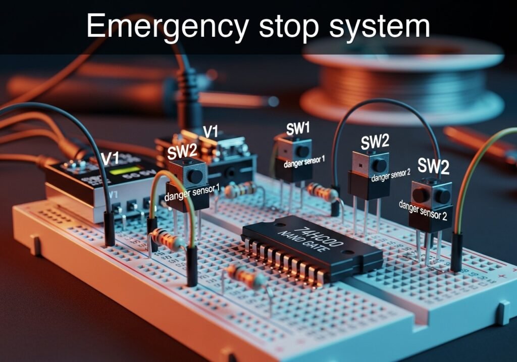
Practical case: Emergency stop system

Emergency stop system prototype (Maker Style)

Level: Basic – Use the low-level output of a NAND gate to stop a process if two sensors detect danger simultaneously.

Objective and use case

In this practical case, you will build a digital safety interlock circuit using a 74HC00 NAND gate. The system evaluates two independent danger sensors and triggers an active-low relay to halt a process only when both sensors detect a critical condition.

Why it is useful:
* Industrial safety: Halting heavy machinery if two separate safety guards are simultaneously bypassed or opened.
* Process control: Triggering an emergency shutdown in a chemical plant if both pressure and temperature exceed critical thresholds.
* Redundant validation: Preventing false alarms from shutting down a system by requiring two independent sensors to agree before taking action.

Expected outcome:
* When both sensors read a HIGH logic level (indicating danger), the NAND gate output will drop to a LOW logic level (~0 V).
* The 0 V signal will trigger an active-low relay module, engaging the emergency stop.
* If either or both sensors read a LOW logic level (safe condition), the NAND output remains HIGH (~5 V), keeping the relay inactive and the process running.

Target audience and level: Beginners in digital electronics and industrial logic control.

Materials

  • V1: 5 V DC power supply
  • SW1: SPST switch, function: danger sensor 1
  • SW2: SPST switch, function: danger sensor 2
  • R1: 10 kΩ resistor, function: pull-down for SW1
  • R2: 10 kΩ resistor, function: pull-down for SW2
  • U1: 74HC00 Quad 2-Input NAND gate IC
  • RLY1: 5 V Active-low relay module, function: process emergency stop

Pin-out of the IC used

We will use the 74HC00 (Quad 2-Input NAND gate).

Pin Name Logic function Connection in this case
1 1 A Input 1 of Gate 1 Node VA (from SW1)
2 1B Input 2 of Gate 1 Node VB (from SW2)
3 1Y Output of Gate 1 Node VOUT (to RLY1 IN)
7 GND Ground Node 0
14 VCC Power Supply Node VCC

Wiring guide

  • V1: connects between node VCC and node 0 (GND).
  • SW1: connects between node VCC and node VA.
  • R1: connects between node VA and node 0.
  • SW2: connects between node VCC and node VB.
  • R2: connects between node VB and node 0.
  • U1: Pin 14 connects to node VCC; Pin 7 connects to node 0.
  • U1: Pin 1 connects to node VA.
  • U1: Pin 2 connects to node VB.
  • U1: Pin 3 connects to node VOUT.
  • RLY1: VCC pin connects to node VCC, GND pin connects to node 0, and the signal/IN pin connects to node VOUT.

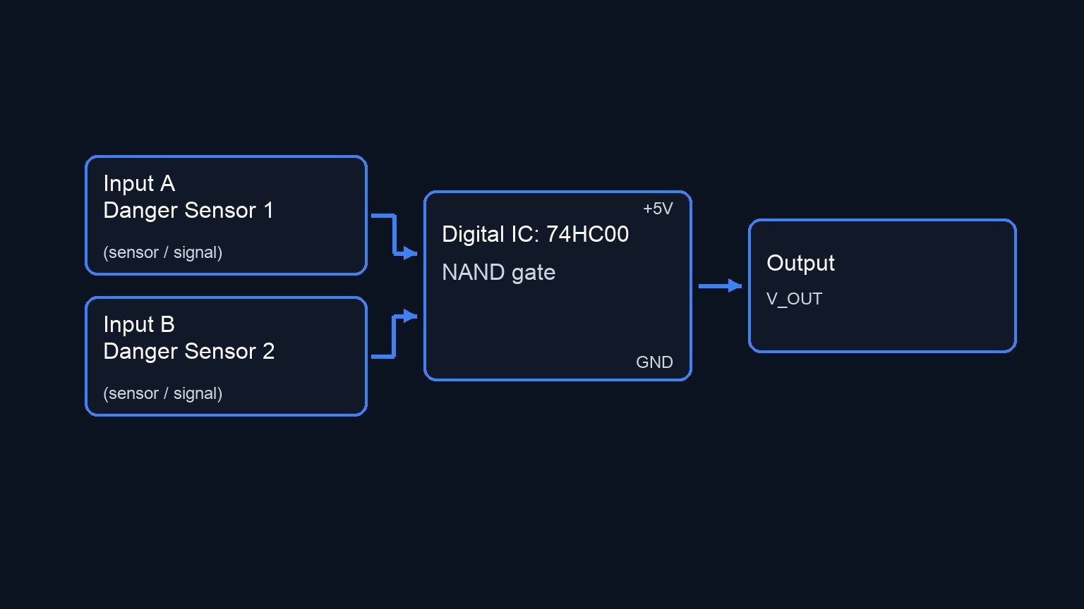
Conceptual block diagram

Conceptual block diagram — 74HC00 NAND gate
Quick read: inputs → main block → output (actuator or measurement). This summarizes the ASCII schematic below.

Schematic

POWER SUPPLY:
[ V1: 5 V DC Power Supply ] --(VCC)
                           --(GND)

SENSOR 1 INPUT PATH:
VCC --> [ SW1: Danger Sensor 1 ] --(Node VA)--> [ U1: 74HC00 NAND (Pin 1) ]
[ Node VA ] --> [ R1: 10 kΩ Pull-down ] --> GND

SENSOR 2 INPUT PATH:
VCC --> [ SW2: Danger Sensor 2 ] --(Node VB)--> [ U1: 74HC00 NAND (Pin 2) ]
[ Node VB ] --> [ R2: 10 kΩ Pull-down ] --> GND

LOGIC TO EMERGENCY STOP PATH:
[ U1: 74HC00 NAND (Pin 3) ] --(Node VOUT)--> [ RLY1: Relay Module (IN) ]

IC & MODULE POWER CONNECTIONS:
VCC --> [ U1: 74HC00 NAND (Pin 14) ]
GND <-- [ U1: 74HC00 NAND (Pin 7) ]

VCC --> [ RLY1: Relay Module (VCC) ]
GND <-- [ RLY1: Relay Module (GND) ]
Electrical Schematic

Truth table

Note: The relay module in this case is active-low, meaning it triggers the emergency stop when it receives a 0.

SW1 (Node VA) SW2 (Node VB) VOUT (NAND Output) Relay State (Active-Low) Process Status
0 (Safe) 0 (Safe) 1 (HIGH) OFF Running
0 (Safe) 1 (Danger) 1 (HIGH) OFF Running
1 (Danger) 0 (Safe) 1 (HIGH) OFF Running
1 (Danger) 1 (Danger) 0 (LOW) ON (Triggered) STOPPED

Measurements and tests

  1. Input Logic States: Using a digital multimeter, measure the DC voltage at nodes VA and VB with respect to node 0. Verify they read ~0 V when the switches are open, and ~5 V when closed.
  2. Output Voltage Level: Measure node VOUT. Confirm it sits near 5 V during normal operation (when one or zero switches are closed).
  3. System Activation: Close both SW1 and SW2 simultaneously. Measure node VOUT to ensure it drops to ~0 V.
  4. Relay Actuation: Listen for the audible «click» of the relay (or observe its onboard indicator LED) precisely when VOUT drops to 0 V, confirming the emergency stop command has been physically executed.

SPICE netlist and simulation

Reference SPICE Netlist (ngspice) — excerptFull SPICE netlist (ngspice)

* Practical case: Emergency stop system
.width out=256

* Main 5V DC power supply
V1 VCC 0 DC 5

* SW1 (Danger sensor 1) and its pull-down resistor
S1 VCC VA ctrl1 0 sw_mod
Vctrl1 ctrl1 0 PULSE(0 5 0 1u 1u 50u 100u)
R1 VA 0 10k

* SW2 (Danger sensor 2) and its pull-down resistor
S2 VCC VB ctrl2 0 sw_mod
Vctrl2 ctrl2 0 PULSE(0 5 0 1u 1u 100u 200u)
R2 VB 0 10k

* U1: 74HC00 Quad 2-Input NAND gate IC (Using pins 1, 2, 3, 7, 14)
XU1 VA VB VOUT VCC 0 NAND_74HC00

* RLY1: 5V Active-low relay module
* ... (truncated in public view) ...

Copy this content into a .cir file and run with ngspice.

* Practical case: Emergency stop system
.width out=256

* Main 5V DC power supply
V1 VCC 0 DC 5

* SW1 (Danger sensor 1) and its pull-down resistor
S1 VCC VA ctrl1 0 sw_mod
Vctrl1 ctrl1 0 PULSE(0 5 0 1u 1u 50u 100u)
R1 VA 0 10k

* SW2 (Danger sensor 2) and its pull-down resistor
S2 VCC VB ctrl2 0 sw_mod
Vctrl2 ctrl2 0 PULSE(0 5 0 1u 1u 100u 200u)
R2 VB 0 10k

* U1: 74HC00 Quad 2-Input NAND gate IC (Using pins 1, 2, 3, 7, 14)
XU1 VA VB VOUT VCC 0 NAND_74HC00

* RLY1: 5V Active-low relay module
XRLY1 VOUT VCC 0 RELAY_MOD

* --- Subcircuits ---

.subckt NAND_74HC00 INA INB OUT VCC GND
* Behavioral NAND gate using continuous sigmoid functions for robust convergence
B1 OUT_int 0 V = 5 * (1 - (1/(1+exp(-20*(V(INA)-2.5)))) * (1/(1+exp(-20*(V(INB)-2.5)))))
R1 OUT_int OUT 100
C1 OUT 0 10p
.ends

.subckt RELAY_MOD IN VCC GND
* Simple resistive model for the relay module to satisfy load requirements
R_in IN GND 10k
R_vcc VCC GND 1k
.ends

* --- Models ---
.model sw_mod SW(Vt=2.5 Ron=0.1 Roff=100Meg)

* --- Analysis Directives ---
.tran 1u 300u
.print tran V(VA) V(VB)
.op
.end

Simulation Results (Transient Analysis)

Simulation Results (Transient Analysis)
Analysis: The ngspice transient analysis shows nodes VA and VB toggling between approximately 0V and 5V, consistent with the PULSE sources driving the switches. This correctly simulates the different combinations of the danger sensors (SW1 and SW2) being triggered or safe.
Show raw data table (501 rows)
Index   time            v(va)           v(vb)
0	0.000000e+00	4.999500e-04	4.999500e-04
1	1.000000e-08	4.999500e-04	4.999500e-04
2	2.000000e-08	4.999500e-04	4.999500e-04
3	4.000000e-08	4.999500e-04	4.999500e-04
4	8.000000e-08	4.999500e-04	4.999500e-04
5	1.600000e-07	4.999500e-04	4.999500e-04
6	3.200000e-07	4.999500e-04	4.999500e-04
7	3.562500e-07	4.999500e-04	4.999500e-04
8	4.196875e-07	4.999500e-04	4.999500e-04
9	4.372461e-07	4.999500e-04	4.999500e-04
10	4.679736e-07	4.999500e-04	4.999500e-04
11	4.795524e-07	4.999500e-04	4.999500e-04
12	4.902290e-07	4.999500e-04	4.999500e-04
13	5.023412e-07	4.999950e+00	4.999950e+00
14	5.111724e-07	4.999950e+00	4.999950e+00
15	5.196372e-07	4.999950e+00	4.999950e+00
16	5.247062e-07	4.999950e+00	4.999950e+00
17	5.271308e-07	4.999950e+00	4.999950e+00
18	5.277087e-07	4.999950e+00	4.999950e+00
19	5.280739e-07	4.999950e+00	4.999950e+00
20	5.285244e-07	4.999950e+00	4.999950e+00
21	5.292184e-07	4.999950e+00	4.999950e+00
22	5.299733e-07	4.999950e+00	4.999950e+00
23	5.306602e-07	4.999950e+00	4.999950e+00
... (477 more rows) ...


Reference SPICE netlist (ngspice)

* Practical case: Emergency stop system
.width out=256

* Main 5V DC power supply
V1 VCC 0 DC 5

* SW1 (Danger sensor 1) and its pull-down resistor
S1 VCC VA ctrl1 0 sw_mod
Vctrl1 ctrl1 0 PULSE(0 5 0 1u 1u 50u 100u)
R1 VA 0 10k

* SW2 (Danger sensor 2) and its pull-down resistor
S2 VCC VB ctrl2 0 sw_mod
Vctrl2 ctrl2 0 PULSE(0 5 0 1u 1u 100u 200u)
R2 VB 0 10k

* U1: 74HC00 Quad 2-Input NAND gate IC (Using pins 1, 2, 3, 7, 14)
XU1 VA VB VOUT VCC 0 NAND_74HC00

* RLY1: 5V Active-low relay module
XRLY1 VOUT VCC 0 RELAY_MOD

* --- Subcircuits ---

.subckt NAND_74HC00 INA INB OUT VCC GND
* Behavioral NAND gate using continuous sigmoid functions for robust convergence
B1 OUT_int 0 V = 5 * (1 - (1/(1+exp(-20*(V(INA)-2.5)))) * (1/(1+exp(-20*(V(INB)-2.5)))))
R1 OUT_int OUT 100
C1 OUT 0 10p
.ends

.subckt RELAY_MOD IN VCC GND
* Simple resistive model for the relay module to satisfy load requirements
R_in IN GND 10k
R_vcc VCC GND 1k
.ends

* --- Models ---
.model sw_mod SW(Vt=2.5 Ron=0.1 Roff=100Meg)

* --- Analysis Directives ---
.tran 1u 300u
.print tran V(VA) V(VB)
.op
.end

Simulation Results (Transient Analysis)

Simulation Results (Transient Analysis)
Analysis: The ngspice transient analysis shows nodes VA and VB toggling between approximately 0V and 5V, consistent with the PULSE sources driving the switches. This correctly simulates the different combinations of the danger sensors (SW1 and SW2) being triggered or safe.

Common mistakes and how to avoid them

  • Floating inputs: Forgetting the pull-down resistors (R1 and R2). Without them, the logic gate inputs will float and pick up ambient noise, causing the relay to trigger randomly.
  • Misunderstanding active-low logic: Expecting the relay to trigger when the output is 5 V. In this case, the NAND output drops to 0 V upon detecting mutual danger, which perfectly matches an active-low relay module. Ensure your relay module is truly active-low.
  • Omitting IC power connections: Forgetting to wire pins 14 (VCC) and 7 (GND) of the 74HC00. The IC will not process logic without power, and may behave erratically if powered parasitically through its input pins.


Troubleshooting

  • Symptom: The relay never clicks, even when both switches are closed.
    • Cause: The 74HC00 output pin cannot sink enough current, or the relay module is active-high instead of active-low.
    • Fix: Ensure you are using a relay module (with a built-in driver transistor) rather than a bare mechanical relay. Verify the module’s trigger logic (some have a jumper to select active-high vs. active-low).
  • Symptom: The relay chatters rapidly or triggers randomly without human interaction.
    • Cause: Floating inputs at node VA or VB.
    • Fix: Double-check that R1 and R2 are properly seated in the breadboard and connected directly to GND (node 0).
  • Symptom: The relay is always ON, and the process is permanently stopped.
    • Cause: The NAND output is permanently stuck at 0 V. This can happen if both inputs are shorted to VCC, or if the logic gate is damaged.
    • Fix: Measure VA and VB. If they are reading 0 V but VOUT is still 0 V, replace the 74HC00 IC.

Possible improvements and extensions

  • Hardware debouncing: Add a 1 µF capacitor across each switch to prevent contact bounce from generating rapid, unintended logic transitions during the millisecond the switch is toggled.
  • Visual status indicators: Connect an LED and a 330 Ω current-limiting resistor to node VOUT to provide a clear visual indicator on a control panel when the system is in a safe state (LED ON) versus an emergency state (LED OFF).

More Practical Cases on Prometeo.blog

Find this product and/or books on this topic on Amazon

Go to Amazon

As an Amazon Associate, I earn from qualifying purchases. If you buy through this link, you help keep this project running.

Quick Quiz

Question 1: What is the main objective of the circuit described in the article?


Question 2: Which specific IC is used in this project?


Question 3: When will the active-low relay be triggered to halt the process?


Question 4: What logic level from the sensors indicates a 'danger' condition?


Question 5: What is the output of the NAND gate when both sensors read a HIGH logic level?


Question 6: What happens to the process if either or both sensors read a LOW logic level (safe condition)?


Question 7: Why is redundant validation useful in this circuit?


Question 8: What is an example of industrial safety mentioned in the text?


Question 9: What type of relay module is used for the process emergency stop?


Question 10: What is the difficulty level of this practical case?


Carlos Núñez Zorrilla
Electronics & Computer Engineer

Telecommunications Electronics Engineer and Computer Engineer (official degrees in Spain).
Follow me:


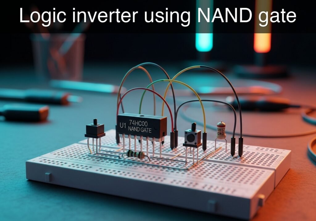
Practical case: Logic inverter using NAND gate

Logic inverter using NAND gate prototype (Maker Style)

Level: Basic – Demonstrate the universality of the NAND gate by configuring it as a basic NOT gate.

Objective and use case

In this practical case, you will build a digital inverter (NOT gate) using a standard 74HC00 NAND gate by shorting its inputs together.

Understanding this configuration is highly useful for several reasons:
* BOM Optimization: It reduces the number of unique integrated circuits needed in a design; if you have spare NAND gates on a board, you do not need to add a dedicated NOT gate chip.
* Logic Universality: It practically proves that NAND gates are «universal,» meaning any logic function can be constructed using only NAND gates.
* Circuit Simplification: It helps streamline routing on printed circuit boards by repurposing nearby unused gates instead of running traces to a different IC.

Expected outcome:
* When the input switch provides a logic LOW (0 V) to the shorted inputs, the output will go HIGH (approx. 5 V), turning on the indicator LED.
* When the input switch provides a logic HIGH (5 V) to the shorted inputs, the output will go LOW (0 V), turning off the indicator LED.
* The circuit will perfectly replicate the behavior of a standard 74HC04 NOT gate.

Target audience: Electronics beginners learning fundamental Boolean algebra and digital hardware implementation.

Materials

  • V1: 5 V DC supply
  • U1: 74HC00 Quad 2-Input NAND Gate
  • SW1: SPST toggle switch or push button, function: input state selector
  • R1: 10 kΩ resistor, function: pull-down for node VA
  • R2: 330 Ω resistor, function: current limiting for the output LED
  • D1: Red LED, function: VOUT state indicator

Pin-out of the IC used

IC: 74HC00 (Quad 2-Input NAND gate)

Pin Name Logic function Connection in this case
1 1 A Input A of Gate 1 Node VA (shorted to 1B)
2 1B Input B of Gate 1 Node VA (shorted to 1 A)
3 1Y Output of Gate 1 Node VOUT
7 GND Ground Node 0
14 VCC Positive Power Supply Node VCC

(Note: Pins 4, 5, 9, 10, 12, 13 are unused inputs in this specific exercise and should ideally be tied to Ground in a final physical circuit to prevent CMOS floating input issues).

Wiring guide

  • V1: Connects between node VCC (+5 V) and node 0 (GND).
  • U1 VCC/GND: Connect pin 14 to node VCC and pin 7 to node 0.
  • SW1: Connects between node VCC and node VA.
  • R1: Connects between node VA and node 0 (ensures a definitive LOW when the switch is open).
  • U1 Inputs: Connect pin 1 (1 A) to node VA and connect pin 2 (1B) to node VA. This ties both inputs of the first NAND gate together.
  • U1 Output: Pin 3 (1Y) provides the inverted signal and connects to node VOUT.
  • R2: Connects between node VOUT and the anode of D1.
  • D1: Connects the cathode to node 0.

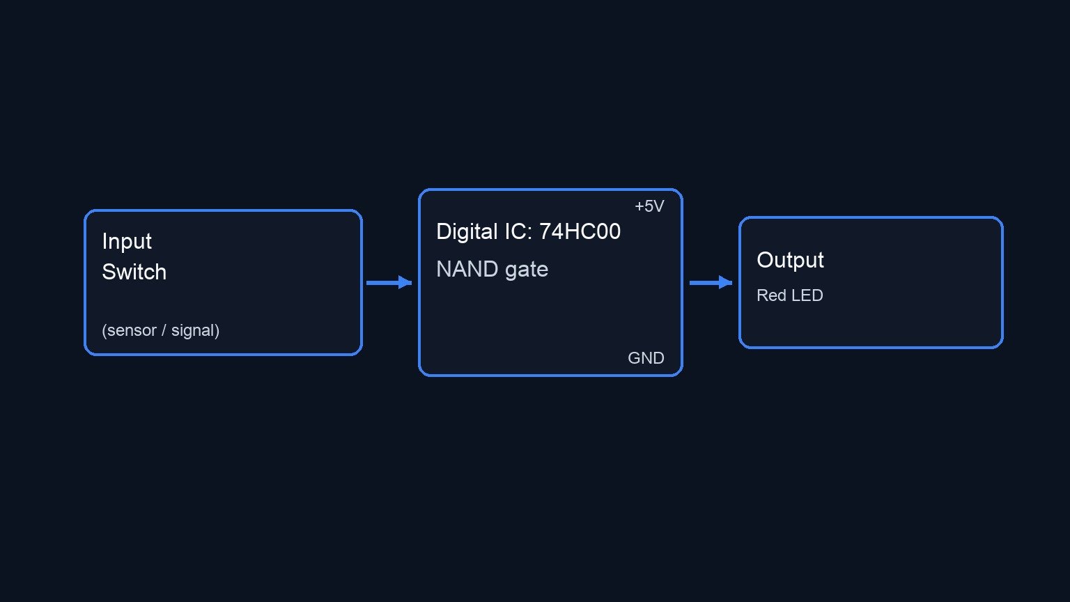
Conceptual block diagram

Conceptual block diagram — 74HC00 NAND gate
Quick read: inputs → main block → output (actuator or measurement). This summarizes the ASCII schematic below.

Schematic

VCC --> [ SW1: Switch ] --(Node VA)--> [ U1: 74HC00 NAND (Pins 1 & 2) ] --(VOUT)--> [ R2: 330 Ω ] --> [ D1: Red LED ] --> GND
                               |
                          [ R1: 10 kΩ ]
                               |
                              GND
Electrical Schematic

Truth table

Input (VA) Output (VOUT) LED State (D1)
0 (LOW) 1 (HIGH) ON
1 (HIGH) 0 (LOW) OFF

Measurements and tests

  1. Input Voltage Measurement: Use a multimeter to measure the voltage at node VA with respect to node 0. Verify that it reads ~0 V when SW1 is open, and ~5 V when SW1 is closed.
  2. Output Voltage Measurement: Move the multimeter probe to node VOUT. Confirm that it reads ~5 V when VA is 0 V, and reads ~0 V when VA is 5 V.
  3. Functional Verification: Toggle the switch multiple times. Ensure D1 behaves inversely to the physical action of the switch (e.g., if pressing the button sends a HIGH signal, the LED should turn off when pressed).

SPICE netlist and simulation

Reference SPICE Netlist (ngspice) — excerptFull SPICE netlist (ngspice)

* Practical case: Logic inverter using NAND gate

* Power Supply
V1 VCC 0 DC 5V

* Switch SW1 (VCC to VA)
* Modeled as a voltage-controlled switch to simulate user interaction
S_SW1 VCC VA SW_CTRL 0 sw_mod
.model sw_mod SW(vt=2.5 vh=0.2 ron=0.1 roff=100Meg)
V_SW_CTRL SW_CTRL 0 PULSE(0 5 10u 1u 1u 100u 200u)

* Pull-down resistor R1
R1 VA 0 10k

* U1: 74HC00 Quad 2-Input NAND Gate (using 1 gate)
* Pin 14: VCC, Pin 7: 0
* Pin 1: VA, Pin 2: VA, Pin 3: VOUT
XU1 VA VA VOUT VCC 0 NAND2_74HC00

* R2: Current limiting resistor
* ... (truncated in public view) ...

Copy this content into a .cir file and run with ngspice.

* Practical case: Logic inverter using NAND gate

* Power Supply
V1 VCC 0 DC 5V

* Switch SW1 (VCC to VA)
* Modeled as a voltage-controlled switch to simulate user interaction
S_SW1 VCC VA SW_CTRL 0 sw_mod
.model sw_mod SW(vt=2.5 vh=0.2 ron=0.1 roff=100Meg)
V_SW_CTRL SW_CTRL 0 PULSE(0 5 10u 1u 1u 100u 200u)

* Pull-down resistor R1
R1 VA 0 10k

* U1: 74HC00 Quad 2-Input NAND Gate (using 1 gate)
* Pin 14: VCC, Pin 7: 0
* Pin 1: VA, Pin 2: VA, Pin 3: VOUT
XU1 VA VA VOUT VCC 0 NAND2_74HC00

* R2: Current limiting resistor
R2 VOUT N1 330

* D1: Red LED
D1 N1 0 DLED

* Models
.model DLED D(IS=1e-15 N=1.8 RS=10)

* Subcircuit for NAND Gate
.subckt NAND2_74HC00 1A 1B 1Y VCC GND
RinA 1A GND 1G
RinB 1B GND 1G
Rvcc VCC GND 100Meg
B1 Y_int GND V = 5 * (1 - (1/(1+exp(-50*(V(1A)-2.5)))) * (1/(1+exp(-50*(V(1B)-2.5)))))
Rout Y_int 1Y 50
.ends

* Analysis
.tran 1u 600u
.print tran V(VA) V(VOUT) V(N1) I(V1)
.op

Simulation Results (Transient Analysis)

Simulation Results (Transient Analysis)
Analysis: The transient simulation shows that when the input VA is LOW (~0V), the output VOUT is HIGH (~4.54V) and the LED node N1 is at ~1.48V (LED ON). When VA goes HIGH (~5V), VOUT goes LOW (~0V) and N1 goes to ~0V (LED OFF). This perfectly matches the expected logic inverter behavior.
Show raw data table (704 rows)
Index   time            v(va)           v(vout)         v(n1)           v1#branch
0	0.000000e+00	4.999400e-04	4.537182e+00	1.482582e+00	-9.99950e-08
1	1.000000e-08	4.999400e-04	4.537182e+00	1.482580e+00	-9.99950e-08
2	2.000000e-08	4.999400e-04	4.537182e+00	1.482580e+00	-9.99950e-08
3	4.000000e-08	4.999400e-04	4.537182e+00	1.482580e+00	-9.99950e-08
4	8.000000e-08	4.999400e-04	4.537182e+00	1.482580e+00	-9.99950e-08
5	1.600000e-07	4.999400e-04	4.537182e+00	1.482580e+00	-9.99950e-08
6	3.200000e-07	4.999400e-04	4.537182e+00	1.482580e+00	-9.99950e-08
7	6.400000e-07	4.999400e-04	4.537182e+00	1.482580e+00	-9.99950e-08
8	1.280000e-06	4.999400e-04	4.537182e+00	1.482580e+00	-9.99950e-08
9	2.280000e-06	4.999400e-04	4.537182e+00	1.482580e+00	-9.99950e-08
10	3.280000e-06	4.999400e-04	4.537182e+00	1.482580e+00	-9.99950e-08
11	4.280000e-06	4.999400e-04	4.537182e+00	1.482580e+00	-9.99950e-08
12	5.280000e-06	4.999400e-04	4.537182e+00	1.482580e+00	-9.99950e-08
13	6.280000e-06	4.999400e-04	4.537182e+00	1.482580e+00	-9.99950e-08
14	7.280000e-06	4.999400e-04	4.537182e+00	1.482580e+00	-9.99950e-08
15	8.280000e-06	4.999400e-04	4.537182e+00	1.482580e+00	-9.99950e-08
16	9.280000e-06	4.999400e-04	4.537182e+00	1.482580e+00	-9.99950e-08
17	1.000000e-05	4.999400e-04	4.537182e+00	1.482580e+00	-9.99950e-08
18	1.010000e-05	4.999400e-04	4.537182e+00	1.482580e+00	-9.99950e-08
19	1.030000e-05	4.999400e-04	4.537182e+00	1.482580e+00	-9.99950e-08
20	1.034750e-05	4.999400e-04	4.537182e+00	1.482580e+00	-9.99950e-08
21	1.043062e-05	4.999400e-04	4.537182e+00	1.482580e+00	-9.99950e-08
22	1.045363e-05	4.999400e-04	4.537182e+00	1.482580e+00	-9.99950e-08
23	1.049390e-05	4.999400e-04	4.537182e+00	1.482580e+00	-9.99950e-08
... (680 more rows) ...


Reference SPICE netlist (ngspice)

* Practical case: Logic inverter using NAND gate

* Power Supply
V1 VCC 0 DC 5V

* Switch SW1 (VCC to VA)
* Modeled as a voltage-controlled switch to simulate user interaction
S_SW1 VCC VA SW_CTRL 0 sw_mod
.model sw_mod SW(vt=2.5 vh=0.2 ron=0.1 roff=100Meg)
V_SW_CTRL SW_CTRL 0 PULSE(0 5 10u 1u 1u 100u 200u)

* Pull-down resistor R1
R1 VA 0 10k

* U1: 74HC00 Quad 2-Input NAND Gate (using 1 gate)
* Pin 14: VCC, Pin 7: 0
* Pin 1: VA, Pin 2: VA, Pin 3: VOUT
XU1 VA VA VOUT VCC 0 NAND2_74HC00

* R2: Current limiting resistor
R2 VOUT N1 330

* D1: Red LED
D1 N1 0 DLED

* Models
.model DLED D(IS=1e-15 N=1.8 RS=10)

* Subcircuit for NAND Gate
.subckt NAND2_74HC00 1A 1B 1Y VCC GND
RinA 1A GND 1G
RinB 1B GND 1G
Rvcc VCC GND 100Meg
B1 Y_int GND V = 5 * (1 - (1/(1+exp(-50*(V(1A)-2.5)))) * (1/(1+exp(-50*(V(1B)-2.5)))))
Rout Y_int 1Y 50
.ends

* Analysis
.tran 1u 600u
.print tran V(VA) V(VOUT) V(N1) I(V1)
.op

Simulation Results (Transient Analysis)

Simulation Results (Transient Analysis)
Analysis: The transient simulation shows that when the input VA is LOW (~0V), the output VOUT is HIGH (~4.54V) and the LED node N1 is at ~1.48V (LED ON). When VA goes HIGH (~5V), VOUT goes LOW (~0V) and N1 goes to ~0V (LED OFF). This perfectly matches the expected logic inverter behavior.

Common mistakes and how to avoid them

  • Leaving CMOS inputs floating: The 74HC00 is a CMOS IC. If you fail to use the pull-down resistor R1, opening SW1 will leave inputs 1 A and 1B floating, leading to erratic output switching and high power consumption. Always use a pull-up or pull-down resistor.
  • Forgetting the LED current limiting resistor: Connecting D1 directly between VOUT and 0 without R2 will draw excessive current, potentially destroying both the LED and the output stage of the 74HC00 IC.
  • Incorrectly shorting inputs: Mistakenly shorting an input to an output (e.g., bridging pins 2 and 3 instead of 1 and 2) will create a feedback loop or logic contention, preventing the circuit from functioning.


Troubleshooting

  • Symptom: The LED never turns on.
    • Cause: The LED (D1) might be inserted backwards, or the IC is unpowered.
    • Fix: Check the polarity of the LED (anode to R2, cathode to 0). Measure the voltage between pins 14 and 7 to confirm the IC is receiving 5 V.
  • Symptom: The LED is always on, regardless of the switch position.
    • Cause: The switch is miswired, or the pull-up/pull-down configuration is incorrect (e.g., node VA is stuck LOW).
    • Fix: Verify that SW1 applies 5 V to node VA when activated. Check R1 for a solid connection to Ground.
  • Symptom: The IC becomes extremely hot.
    • Cause: Power supply is reversed or there is a dead short at the output.
    • Fix: Immediately disconnect power. Verify that pin 14 goes to VCC and pin 7 goes to 0. Ensure R2 is present in the output path.

Possible improvements and extensions

  • Add an Input Indicator: Connect a second LED and resistor directly to node VA. This allows you to visually compare the input state and output state side-by-side (when one LED is ON, the other will be OFF).
  • Build an AND Gate: Cascade this newly built inverter into a second NAND gate. Connect the output of a standard NAND gate to the shorted inputs of your NAND-based NOT gate to create a functional AND gate, further demonstrating universal logic.

More Practical Cases on Prometeo.blog

Find this product and/or books on this topic on Amazon

Go to Amazon

As an Amazon Associate, I earn from qualifying purchases. If you buy through this link, you help keep this project running.

Quick Quiz

Question 1: What is the main objective of the practical case described in the article?


Question 2: Which specific integrated circuit is mentioned for building the digital inverter?


Question 3: How is the NAND gate configured to act as a NOT gate?


Question 4: What does the term 'Logic Universality' mean in the context of NAND gates?


Question 5: How does using a NAND gate as a NOT gate help with BOM (Bill of Materials) optimization?


Question 6: What is the expected output when the input switch provides a logic LOW (0 V) to the shorted inputs?


Question 7: What happens to the indicator LED when a logic HIGH (5 V) is provided to the inputs?


Question 8: How does repurposing unused NAND gates benefit printed circuit board (PCB) design?


Question 9: What logic level corresponds to approximately 5 V in this practical case?


Question 10: What behavior does the configured 74HC00 circuit perfectly replicate?


Carlos Núñez Zorrilla
Electronics & Computer Engineer

Telecommunications Electronics Engineer and Computer Engineer (official degrees in Spain).
Follow me:


Practical case: Dual Input Alarm System using OR Gate

Dual Input Alarm System using OR Gate prototype (Maker Style)

Level: Basic – Build an alert system that activates a warning LED when either a local or remote signal is triggered.

Objective and use case

In this practical case, you will build a digital alarm indicator utilizing a 74HC32 logic OR gate. The circuit combines two independent input signals (representing a local sensor and a remote sensor) so that if either one or both are activated, the output will drive an alert LED.

Why this circuit is useful:
* Security systems: A single alarm panel can monitor both a front door and a back door.
* Industrial safety: A machine can be halted by either a local emergency stop button or a remote operator console.
* Environmental monitoring: A system can trigger a unified warning if either a smoke detector or a heat sensor detects an anomaly.

Expected outcome:
* With both switches open (0 V at inputs), the output is 0 V and the LED is off.
* Closing the local switch yields 5 V at the first input, forcing the output to 5 V and turning on the LED.
* Closing the remote switch yields 5 V at the second input, forcing the output to 5 V and turning on the LED.
* Closing both switches simultaneously yields 5 V at both inputs, maintaining the 5 V output and keeping the LED illuminated.

Target audience and level: Beginners and hobbyists learning basic digital logic concepts.

Materials

  • U1: 74HC32 quad 2-input OR gate, function: logic control
  • V1: 5 V DC supply, function: power source
  • SW1: SPST switch, function: local alarm trigger
  • SW2: SPST switch, function: remote alarm trigger
  • R1: 10 kΩ resistor, function: pull-down for VA
  • R2: 10 kΩ resistor, function: pull-down for VB
  • R3: 330 Ω resistor, function: LED current limiting
  • D1: red LED, function: alarm indicator

Pin-out of the IC used

74HC32 (Quad 2-input OR gate)

Pin Name Logic function Connection in this case
1 1 A Input 1 for Gate 1 Connects to node VA (from SW1)
2 1B Input 2 for Gate 1 Connects to node VB (from SW2)
3 1Y Output of Gate 1 Connects to node VOUT
7 GND Ground / 0 V reference Connects to node 0
14 VCC Positive supply voltage Connects to node VCC

(Note: Pins 4, 5, 6, 8, 9, 10, 11, 12, and 13 belong to the other three unused OR gates in the package and should ideally have their inputs tied to ground in a permanent design, though they are left out of this primary signal path for simplicity).

Wiring guide

  • V1: Positive terminal connects to node VCC, negative terminal connects to node 0.
  • SW1: Connects between node VCC and node VA.
  • SW2: Connects between node VCC and node VB.
  • R1: Connects between node VA and node 0.
  • R2: Connects between node VB and node 0.
  • U1: Pin 14 connects to node VCC, Pin 7 connects to node 0. Pin 1 connects to node VA, Pin 2 connects to node VB, Pin 3 connects to node VOUT.
  • R3: Connects between node VOUT and node VLED.
  • D1: Anode connects to node VLED, cathode connects to node 0.

Conceptual block diagram

Conceptual block diagram — PUERTA OR gate
Quick read: inputs → main block → output (actuator or measurement). This summarizes the ASCII schematic below.

Schematic

VCC --> [ SW1: Local Alarm ] --(VA)-->+---------------------------------> [           ]
                                      |                                   [ U1: Pin 1 ]
                                      +--> [ R1: 10 kΩ Pull-down ] --> GND [           ]
                                                                          [  74HC32   ] --(VOUT)--> [ R3: 330 Ω ] --(VLED)--> [ D1: Red LED ] --> GND
VCC --> [ SW2: Remote Alarm] --(VB)-->+---------------------------------> [  OR Gate  ]
                                      |                                   [           ]
                                      +--> [ R2: 10 kΩ Pull-down ] --> GND [ U1: Pin 2 ]
                                                                          [           ]
Electrical Schematic

Truth table

Local Signal (VA) Remote Signal (VB) Output (VOUT) Alarm LED (D1)
0 (Low) 0 (Low) 0 (Low) OFF
0 (Low) 1 (High) 1 (High) ON
1 (High) 0 (Low) 1 (High) ON
1 (High) 1 (High) 1 (High) ON

Measurements and tests

  1. Input Verification: Using a digital multimeter (DMM) referenced to node 0, measure the voltage at nodes VA and VB. Verify that they read approximately 0 V when the respective switch is open, and 5 V when closed.
  2. Output Verification: Measure the voltage at node VOUT. Confirm that it reads 0 V only when both VA and VB are at 0 V. If either or both inputs are at 5 V, VOUT must measure close to 5 V.
  3. Visual Confirmation: Toggle SW1 and SW2 through all four possible combinations as listed in the truth table and confirm D1 behaves accordingly.
  4. Current Measurement (Optional): Place your DMM in series with R3 to measure the LED forward current. It should be approximately 8-10 mA depending on the LED’s forward voltage drop.

SPICE netlist and simulation

Reference SPICE Netlist (ngspice) — excerptFull SPICE netlist (ngspice)

* Dual Input Alarm System using OR Gate
.width out=256

* Power Supply
V1 VCC 0 DC 5

* Local Alarm Trigger (SW1)
* Modeled as a voltage-controlled switch driven by a pulse to simulate user interaction
SW1 VCC VA ctrl1 0 mySW
Vctrl1 ctrl1 0 PULSE(0 5 0 1u 1u 50u 100u)

* Remote Alarm Trigger (SW2)
* Modeled as a voltage-controlled switch driven by a pulse to simulate user interaction
SW2 VCC VB ctrl2 0 mySW
Vctrl2 ctrl2 0 PULSE(0 5 0 1u 1u 100u 200u)

* Switch Model
.model mySW SW(Ron=1 Roff=100Meg Vt=2.5)

* Pull-down resistors
* ... (truncated in public view) ...

Copy this content into a .cir file and run with ngspice.

* Dual Input Alarm System using OR Gate
.width out=256

* Power Supply
V1 VCC 0 DC 5

* Local Alarm Trigger (SW1)
* Modeled as a voltage-controlled switch driven by a pulse to simulate user interaction
SW1 VCC VA ctrl1 0 mySW
Vctrl1 ctrl1 0 PULSE(0 5 0 1u 1u 50u 100u)

* Remote Alarm Trigger (SW2)
* Modeled as a voltage-controlled switch driven by a pulse to simulate user interaction
SW2 VCC VB ctrl2 0 mySW
Vctrl2 ctrl2 0 PULSE(0 5 0 1u 1u 100u 200u)

* Switch Model
.model mySW SW(Ron=1 Roff=100Meg Vt=2.5)

* Pull-down resistors
R1 VA 0 10k
R2 VB 0 10k

* 74HC32 Quad 2-input OR gate (using 1 gate)
XU1 VA VB VOUT 0 VCC U_74HC32_OR

* Robust Subcircuit for 74HC32 OR Gate using continuous math functions
.subckt U_74HC32_OR P1 P2 P3 P7 P14
B1 P3 P7 V = V(P14,P7) * (1 - (1 / (1 + exp(50*(V(P1,P7)-V(P14,P7)/2)))) * (1 / (1 + exp(50*(V(P2,P7)-V(P14,P7)/2)))))
.ends

* Output Indicator
R3 VOUT VLED 330
D1 VLED 0 DLED
.model DLED D(IS=1e-15 N=1.8 RS=10)

* Analysis Commands
.tran 1u 300u
.print tran V(VA) V(VB) V(VOUT) V(VLED)
.op

Simulation Results (Transient Analysis)

Simulation Results (Transient Analysis)
Analysis: The transient analysis spans 0 s to 300 us and captures the switching interval. Main ranges: v(vout) 2.77e-62 uV -> 5 V; v(va) 500 uV -> 5 V; v(vb) 500 uV -> 5 V.
Show raw data table (412 rows)
Index   time            v(va)           v(vb)           v(vout)         v(vled)
0	0.000000e+00	4.999500e-04	4.999500e-04	2.767481e-68	5.488664e-30
1	1.000000e-08	4.999500e-04	4.999500e-04	2.767481e-68	4.008316e-41
2	2.000000e-08	4.999500e-04	4.999500e-04	2.767481e-68	-4.00832e-41
3	4.000000e-08	4.999500e-04	4.999500e-04	2.767481e-68	-1.46362e-51
4	8.000000e-08	4.999500e-04	4.999500e-04	2.767481e-68	5.854466e-52
5	1.600000e-07	4.999500e-04	4.999500e-04	2.767481e-68	3.420369e-62
6	3.200000e-07	4.999500e-04	4.999500e-04	2.767481e-68	-8.55089e-63
7	3.562500e-07	4.999500e-04	4.999500e-04	2.767481e-68	2.767467e-68
8	4.196875e-07	4.999500e-04	4.999500e-04	2.767481e-68	2.767492e-68
9	4.372461e-07	4.999500e-04	4.999500e-04	2.767481e-68	2.767481e-68
10	4.679736e-07	4.999500e-04	4.999500e-04	2.767481e-68	2.767481e-68
11	5.019934e-07	4.999500e+00	4.999500e+00	5.000000e+00	1.503225e+00
12	5.700330e-07	4.999500e+00	4.999500e+00	5.000000e+00	1.502641e+00
13	7.061121e-07	4.999500e+00	4.999500e+00	5.000000e+00	1.502321e+00
14	9.782703e-07	4.999500e+00	4.999500e+00	5.000000e+00	1.502318e+00
15	1.000000e-06	4.999500e+00	4.999500e+00	5.000000e+00	1.502314e+00
16	1.043459e-06	4.999500e+00	4.999500e+00	5.000000e+00	1.502314e+00
17	1.130378e-06	4.999500e+00	4.999500e+00	5.000000e+00	1.502314e+00
18	1.304216e-06	4.999500e+00	4.999500e+00	5.000000e+00	1.502314e+00
19	1.651892e-06	4.999500e+00	4.999500e+00	5.000000e+00	1.502314e+00
20	2.347244e-06	4.999500e+00	4.999500e+00	5.000000e+00	1.502314e+00
21	3.347244e-06	4.999500e+00	4.999500e+00	5.000000e+00	1.502314e+00
22	4.347244e-06	4.999500e+00	4.999500e+00	5.000000e+00	1.502314e+00
23	5.347244e-06	4.999500e+00	4.999500e+00	5.000000e+00	1.502314e+00
... (388 more rows) ...


Reference SPICE netlist (ngspice)

* Dual Input Alarm System using OR Gate
.width out=256

* Power Supply
V1 VCC 0 DC 5

* Local Alarm Trigger (SW1)
* Modeled as a voltage-controlled switch driven by a pulse to simulate user interaction
SW1 VCC VA ctrl1 0 mySW
Vctrl1 ctrl1 0 PULSE(0 5 0 1u 1u 50u 100u)

* Remote Alarm Trigger (SW2)
* Modeled as a voltage-controlled switch driven by a pulse to simulate user interaction
SW2 VCC VB ctrl2 0 mySW
Vctrl2 ctrl2 0 PULSE(0 5 0 1u 1u 100u 200u)

* Switch Model
.model mySW SW(Ron=1 Roff=100Meg Vt=2.5)

* Pull-down resistors
R1 VA 0 10k
R2 VB 0 10k

* 74HC32 Quad 2-input OR gate (using 1 gate)
XU1 VA VB VOUT 0 VCC U_74HC32_OR

* Robust Subcircuit for 74HC32 OR Gate using continuous math functions
.subckt U_74HC32_OR P1 P2 P3 P7 P14
B1 P3 P7 V = V(P14,P7) * (1 - (1 / (1 + exp(50*(V(P1,P7)-V(P14,P7)/2)))) * (1 / (1 + exp(50*(V(P2,P7)-V(P14,P7)/2)))))
.ends

* Output Indicator
R3 VOUT VLED 330
D1 VLED 0 DLED
.model DLED D(IS=1e-15 N=1.8 RS=10)

* Analysis Commands
.tran 1u 300u
.print tran V(VA) V(VB) V(VOUT) V(VLED)
.op

Simulation Results (Transient Analysis)

Simulation Results (Transient Analysis)
Analysis: The transient analysis spans 0 s to 300 us and captures the switching interval. Main ranges: v(vout) 2.77e-62 uV -> 5 V; v(va) 500 uV -> 5 V; v(vb) 500 uV -> 5 V.

Common mistakes and how to avoid them

  1. Floating inputs: Forgetting to connect the pull-down resistors (R1 and R2). Without them, when the switches are open, the 74HC32 inputs act like antennas and will cause the output to randomly toggle or oscillate. Always use pull-down resistors.
  2. Missing LED current limiting resistor: Connecting the LED directly from the output pin (node VOUT) to ground. This will draw excessive current, potentially burning out both the LED and the 74HC32 output stage. Always include R3.
  3. Forgetting IC power connections: Wiring the inputs and outputs but forgetting to supply VCC to pin 14 and GND to pin 7. The IC cannot function without its power rails connected.


Troubleshooting

  • Symptom: The LED is always ON, regardless of switch positions.
    • Cause: Inputs are permanently shorted to VCC, or switches are wired as «Normally Closed».
    • Fix: Verify that the switches only bridge VCC to the inputs when actively pressed. Ensure nodes VA and VB measure 0 V when switches are released.
  • Symptom: The LED never turns ON.
    • Cause: LED D1 is inserted backwards (reversed polarity), or the IC is not powered.
    • Fix: Check the orientation of D1 (anode to R3, cathode to ground). Measure pin 14 on U1 to guarantee it receives 5 V.
  • Symptom: The LED flickers when you move your hand near the circuit.
    • Cause: The inputs are floating. CMOS chips have highly sensitive inputs.
    • Fix: Check the connections of R1 and R2. Ensure they securely tie nodes VA and VB to ground when the switches are open.

Possible improvements and extensions

  1. Audible alert integration: Add an active 5 V piezoelectric buzzer in parallel with the LED/resistor combination (connecting the buzzer’s positive lead to VOUT and the negative lead to node 0) to provide both a visual and audible alarm.
  2. Expand to a 3-input alarm: Utilize a second OR gate inside the same 74HC32 chip. Connect VOUT to Pin 4 (2 A), a third switch/pull-down assembly to Pin 5 (2B), and use Pin 6 (2Y) to drive the LED, creating a system that monitors three distinct zones.

More Practical Cases on Prometeo.blog

Find this product and/or books on this topic on Amazon

Go to Amazon

As an Amazon Associate, I earn from qualifying purchases. If you buy through this link, you help keep this project running.

Quick Quiz

Question 1: What is the main logic gate used in this alert system?


Question 2: What condition turns the warning LED off?


Question 3: What voltage represents an open switch at the inputs in this circuit?


Question 4: What happens to the LED if only the local switch is closed?


Question 5: Which of the following is a mentioned use case for this circuit?


Question 6: In the environmental monitoring example, what two sensors are combined?


Question 7: What is the output voltage when both switches are closed simultaneously?


Question 8: How many independent input signals does this specific circuit combine?


Question 9: What does the output of the 74HC32 gate drive in this practical case?


Question 10: In a security system application, what could the two inputs represent?


Carlos Núñez Zorrilla
Electronics & Computer Engineer

Telecommunications Electronics Engineer and Computer Engineer (official degrees in Spain).

Follow me: