Practical case: Intrusion alarm by wire break

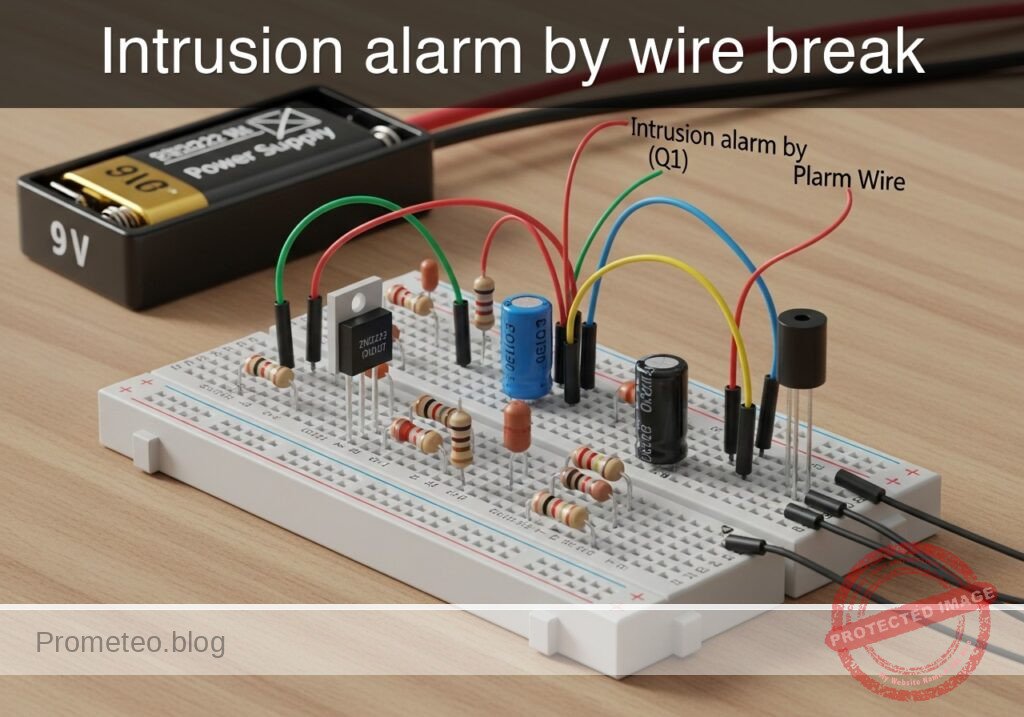
Intrusion alarm by wire break prototype (Maker Style)

Level: Basic. Design a security circuit where cutting a wire activates an alarm using transistor saturation logic.

Objective and use case

In this project, you will build a closed-loop security system using a BJT transistor. When a specific wire (the «sense loop») is intact, the system remains silent; if the wire is cut or disconnected, an LED lights up immediately.

  • Perimeter security: Monitor windows or fences where a conductive strip or wire is installed.
  • Anti-tamper mechanisms: Detect if a device case has been opened by breaking a connection.
  • Continuity testing: Verify cable integrity in manufacturing harnesses.

Expected outcome:
* Loop Intact (Secure): The LED remains OFF. VBE ≈ 0 V.
* Loop Cut (Alarm): The LED turns ON. VBE ≈ 0.7 V and the transistor enters saturation (VCE < 0.2 V).

Target audience: Students and hobbyists learning basic transistor switching applications.

Materials

  • V1: 9 V DC power supply or battery.
  • Q1: 2N2222 or BC547 (NPN BJT), function: electronic switch.
  • R1: 10 kΩ resistor, function: base pull-up resistor.
  • R2: 470 Ω resistor, function: LED current limiting.
  • D1: Red LED, function: visual alarm indicator.
  • W1: Copper wire or jumper, function: sense loop (the «intruder» wire).

Wiring guide

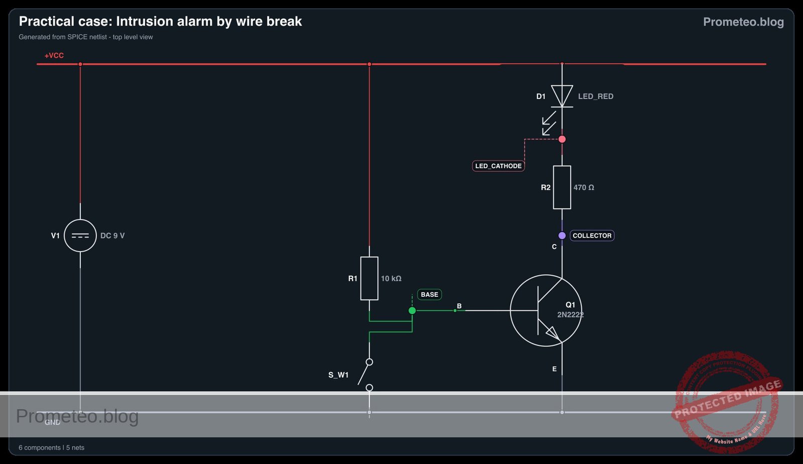
Construct the circuit ensuring all connections map to the following nodes: VCC, GND (0), BASE, and COLLECTOR.

  • V1: Positive terminal to VCC, Negative terminal to GND.
  • R1 (Pull-up): Connects between VCC and BASE.
  • W1 (Sense Loop): Connects between BASE and GND.
  • Q1 (Transistor):
    • Base pin to BASE.
    • Emitter pin to GND.
    • Collector pin to COLLECTOR.
  • D1 (LED): Anode to VCC, Cathode to node LED_CATHODE.
  • R2 (Limiting): Connects between LED_CATHODE and COLLECTOR.

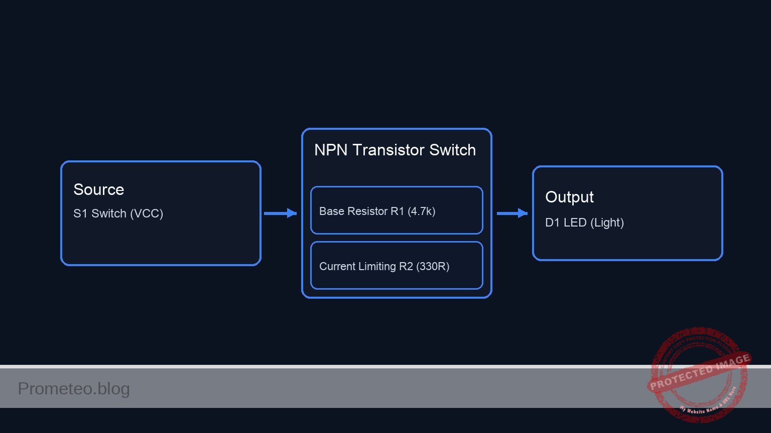
Conceptual block diagram

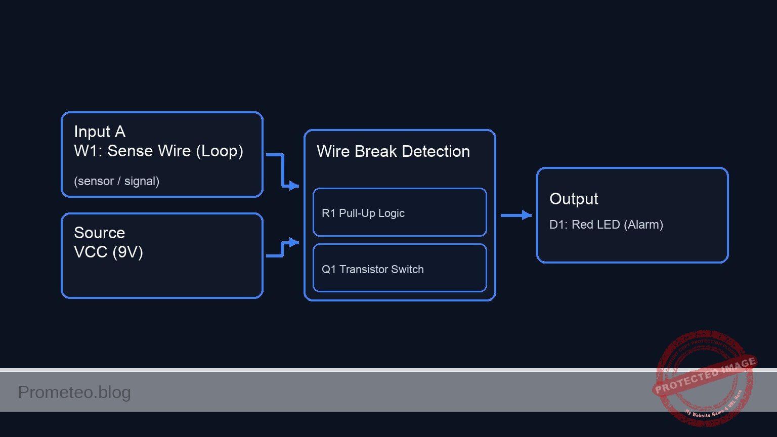
Conceptual block diagram — Wire Break Detection
Quick read: inputs → main block → output (actuator or measurement). This summarizes the ASCII schematic below.

Schematic

Title: Practical case: Intrusion alarm by wire break

[ A. CONTROL / SENSING LOOP ]
(Logic: W1 keeps Base LOW. If W1 breaks, R1 pulls Base HIGH)

VCC (9 V) --> [ R1: 10k Pull-Up ] --(Node: BASE)--> [ Q1: Base ]
                                         |
                                         +-------> [ W1: Sense Wire ] --> GND


[ B. ALARM / POWER LOOP ]
(Logic: Current flows through LED only when Q1 is ON)

VCC (9 V) --> [ D1: Red LED ] --> [ R2: 470R ] --> [ Q1: Collector ]
                                                          |
                                                      (Switch)
                                                          |
                                                          v
                                                   [ Q1: Emitter ] --> GND
Schematic (ASCII)

Electrical diagram

Electrical diagram for case: Intrusion alarm by wire break
Generated from the validated SPICE netlist for this case.

🔒 This electrical diagram is premium. With the monthly membership (7-day free trial) you can unlock the complete didactic material and the print-ready PDF pack.🔓 See premium access plans

Measurements and tests

Verify the logic states using a multimeter.

  1. State 1: Loop Intact (Secure)

    • Ensure the wire W1 connects BASE to GND.
    • Measure Voltage Base-Emitter (VBE): Should be 0 V.
    • Measure Voltage Collector-Emitter (VCE): Should be close to 9 V (Cut-off region).
    • Result: LED is OFF.
  2. State 2: Loop Broken (Alarm)

    • Disconnect or cut wire W1.
    • Measure Voltage Base-Emitter (VBE): Should be approximately 0.7 V.
    • Measure Voltage Collector-Emitter (VCE): Should be approximately 0.1 V to 0.2 V (Saturation region).
    • Result: LED is ON.

SPICE netlist and simulation

Reference SPICE Netlist (ngspice) — excerptFull SPICE netlist (ngspice)

* Practical case: Intrusion alarm by wire break
.width out=256

* --- Power Supply ---
* V1: 9 V DC power supply
V1 VCC 0 DC 9

* --- Input / Sense Loop ---
* W1: Sense Loop (Copper wire). 
* Modeled as a Voltage Controlled Switch (S_W1) to simulate the wire breaking.
* Logic: High Control (5V) = Wire Intact (Closed). Low Control (0V) = Wire Broken (Open).
S_W1 BASE 0 CTRL 0 SW_WIRE
.model SW_WIRE SW(Vt=2.5 Vh=0.1 Ron=0.01 Roff=100Meg)

* Control Signal for W1:
* Starts at 5V (Intact), breaks at 2ms (0V), stays broken for duration.
V_W1_CTRL CTRL 0 PULSE(5 0 2ms 1u 1u 5ms 10ms)

* --- Pull-up Network ---
* R1: Base pull-up resistor
* ... (truncated in public view) ...

Copy this content into a .cir file and run with ngspice.

🔒 Part of this section is premium. With the monthly membership (7-day free trial) you can access the full content (materials, wiring, detailed build, validation, troubleshooting, variants and checklist) and download the complete print-ready PDF pack.

* Practical case: Intrusion alarm by wire break
.width out=256

* --- Power Supply ---
* V1: 9 V DC power supply
V1 VCC 0 DC 9

* --- Input / Sense Loop ---
* W1: Sense Loop (Copper wire). 
* Modeled as a Voltage Controlled Switch (S_W1) to simulate the wire breaking.
* Logic: High Control (5V) = Wire Intact (Closed). Low Control (0V) = Wire Broken (Open).
S_W1 BASE 0 CTRL 0 SW_WIRE
.model SW_WIRE SW(Vt=2.5 Vh=0.1 Ron=0.01 Roff=100Meg)

* Control Signal for W1:
* Starts at 5V (Intact), breaks at 2ms (0V), stays broken for duration.
V_W1_CTRL CTRL 0 PULSE(5 0 2ms 1u 1u 5ms 10ms)

* --- Pull-up Network ---
* R1: Base pull-up resistor
R1 VCC BASE 10k

* --- Switching Element ---
* Q1: NPN Transistor (2N2222)
* Connections: Collector, Base, Emitter(GND)
Q1 COLLECTOR BASE 0 2N2222
.model 2N2222 NPN(IS=1E-14 VAF=100 BF=200 IKF=0.3 XTB=1.5 BR=3 CJC=8E-12 CJE=25E-12 TR=46.91E-9 TF=411.1E-12 ITF=0.6 VTF=1.7 XTF=3 RB=10 RC=0.3 RE=0.2)

* --- Output / Alarm Indicator ---
* D1: Red LED
* Anode to VCC, Cathode to LED_CATHODE
D1 VCC LED_CATHODE LED_RED
.model LED_RED D(IS=93.2P RS=42M N=3.73 BV=4 IBV=10U CJO=2.97P VJ=0.75 M=0.33 TT=4.32U)

* R2: LED current limiting resistor
* Between LED_CATHODE and COLLECTOR
R2 LED_CATHODE COLLECTOR 470

* --- Simulation Commands ---
.op
* Simulate for 5ms to capture the wire break event at 2ms
.tran 10u 5ms

* --- Output Printing ---
* V(BASE): Trigger voltage (Low=Intact, High=Alarm)
* V(COLLECTOR): Output node (Pulled Low when Alarm is Active)
.print tran V(BASE) V(COLLECTOR) V(LED_CATHODE)

.end

Simulation Results (Transient Analysis)

Simulation Results (Transient Analysis)
Show raw data table (536 rows)
Index   time            v(base)         v(collector)    v(led_cathode)
0	0.000000e+00	8.999991e-06	8.979590e+00	8.979590e+00
1	1.000000e-07	8.999991e-06	8.979590e+00	8.979590e+00
2	2.000000e-07	8.999991e-06	8.979590e+00	8.979590e+00
3	4.000000e-07	8.999991e-06	8.979590e+00	8.979590e+00
4	8.000000e-07	8.999991e-06	8.979590e+00	8.979590e+00
5	1.600000e-06	8.999991e-06	8.979591e+00	8.979591e+00
6	3.200000e-06	8.999991e-06	8.979592e+00	8.979592e+00
7	6.400000e-06	8.999991e-06	8.979594e+00	8.979594e+00
8	1.280000e-05	8.999991e-06	8.979598e+00	8.979598e+00
9	2.280000e-05	8.999991e-06	8.979604e+00	8.979604e+00
10	3.280000e-05	8.999991e-06	8.979610e+00	8.979610e+00
11	4.280000e-05	8.999991e-06	8.979616e+00	8.979616e+00
12	5.280000e-05	8.999991e-06	8.979622e+00	8.979623e+00
13	6.280000e-05	8.999991e-06	8.979629e+00	8.979629e+00
14	7.280000e-05	8.999991e-06	8.979635e+00	8.979635e+00
15	8.280000e-05	8.999991e-06	8.979641e+00	8.979641e+00
16	9.280000e-05	8.999991e-06	8.979647e+00	8.979647e+00
17	1.028000e-04	8.999991e-06	8.979653e+00	8.979653e+00
18	1.128000e-04	8.999991e-06	8.979659e+00	8.979659e+00
19	1.228000e-04	8.999991e-06	8.979665e+00	8.979665e+00
20	1.328000e-04	8.999991e-06	8.979671e+00	8.979671e+00
21	1.428000e-04	8.999991e-06	8.979677e+00	8.979677e+00
22	1.528000e-04	8.999991e-06	8.979684e+00	8.979684e+00
23	1.628000e-04	8.999991e-06	8.979690e+00	8.979690e+00
... (512 more rows) ...


Reference SPICE netlist (ngspice)

* Practical case: Intrusion alarm by wire break
.width out=256

* --- Power Supply ---
* V1: 9 V DC power supply
V1 VCC 0 DC 9

* --- Input / Sense Loop ---
* W1: Sense Loop (Copper wire).
* Modeled as a Voltage Controlled Switch (S_W1) to simulate the wire breaking.
* Logic: High Control (5V) = Wire Intact (Closed). Low Control (0V) = Wire Broken (Open).
S_W1 BASE 0 CTRL 0 SW_WIRE
.model SW_WIRE SW(Vt=2.5 Vh=0.1 Ron=0.01 Roff=100Meg)

* Control Signal for W1:
* Starts at 5V (Intact), breaks at 2ms (0V), stays broken for duration.
V_W1_CTRL CTRL 0 PULSE(5 0 2ms 1u 1u 5ms 10ms)

* --- Pull-up Network ---
* R1: Base pull-up resistor
R1 VCC BASE 10k

* --- Switching Element ---
* Q1: NPN Transistor (2N2222)
* Connections: Collector, Base, Emitter(GND)
Q1 COLLECTOR BASE 0 2N2222
.model 2N2222 NPN(IS=1E-14 VAF=100 BF=200 IKF=0.3 XTB=1.5 BR=3 CJC=8E-12 CJE=25E-12 TR=46.91E-9 TF=411.1E-12 ITF=0.6 VTF=1.7 XTF=3 RB=10 RC=0.3 RE=0.2)

* --- Output / Alarm Indicator ---
* D1: Red LED
* Anode to VCC, Cathode to LED_CATHODE
D1 VCC LED_CATHODE LED_RED
.model LED_RED D(IS=93.2P RS=42M N=3.73 BV=4 IBV=10U CJO=2.97P VJ=0.75 M=0.33 TT=4.32U)

* R2: LED current limiting resistor
* Between LED_CATHODE and COLLECTOR
R2 LED_CATHODE COLLECTOR 470

* --- Simulation Commands ---
.op
* Simulate for 5ms to capture the wire break event at 2ms
.tran 10u 5ms

* --- Output Printing ---
* V(BASE): Trigger voltage (Low=Intact, High=Alarm)
* V(COLLECTOR): Output node (Pulled Low when Alarm is Active)
.print tran V(BASE) V(COLLECTOR) V(LED_CATHODE)

.end

Simulation Results (Transient Analysis)

Simulation Results (Transient Analysis)

Common mistakes and how to avoid them

  1. Connecting the loop to the Collector: Placing the sense wire on the output side will likely short the power supply or the LED, rather than controlling the transistor. Ensure the loop controls the Base.
  2. Omitting the Base Resistor (R1): If R1 is missing, the Base floats when the wire is cut, and the transistor may not turn on reliably. R1 provides the necessary turn-on current.
  3. No current limiting for LED: Forgetting R2 allows unlimited current to flow through the LED and Q1 upon alarm activation, instantly burning out the LED.

Troubleshooting

  • LED never turns ON: Check if R1 is connected to VCC. If the base never receives voltage when the wire is cut, the transistor stays OFF.
  • LED stays ON (even with loop intact): Check the W1 connection. If the resistance of the sense wire is too high (bad contact), it might not pull the base voltage down enough to turn off the transistor.
  • Transistor gets hot: Check if R2 is too low (excessive collector current) or if the LED is shorted.

Possible improvements and extensions

  1. Audible Alarm: Connect a 9 V active buzzer in parallel with the LED (and its resistor) to provide sound.
  2. Latching Circuit: Use a Thyristor (SCR) instead of an NPN transistor so that once the wire is cut, the alarm stays ON even if the intruder tries to reconnect the wire.

More Practical Cases on Prometeo.blog

Find this product and/or books on this topic on Amazon

Go to Amazon

As an Amazon Associate, I earn from qualifying purchases. If you buy through this link, you help keep this project running.

Quick Quiz

Question 1: What is the primary function of the 'sense loop' wire in this security circuit?


Question 2: When the sense loop is intact (secure state), what is the status of the LED?


Question 3: Which component acts as the electronic switch in this circuit?


Question 4: What happens electrically when the sense wire (W1) is cut?


Question 5: What is the approximate Base-Emitter voltage (Vbe) when the alarm is triggered (Loop Cut)?


Question 6: In the 'Secure' state (Loop Intact), why is the Base-Emitter voltage approximately 0 V?


Question 7: What is the purpose of resistor R2 (470R) in the Alarm/Power Loop?


Question 8: Which resistor acts as the 'Pull-Up' resistor for the base of the transistor?


Question 9: What transistor state corresponds to the 'Alarm' condition?


Question 10: Which of the following is a listed use case for this circuit?


Carlos Núñez Zorrilla
Electronics & Computer Engineer

Telecommunications Electronics Engineer and Computer Engineer (official degrees in Spain).
Follow me:


Practical case: Slow turn-off timer

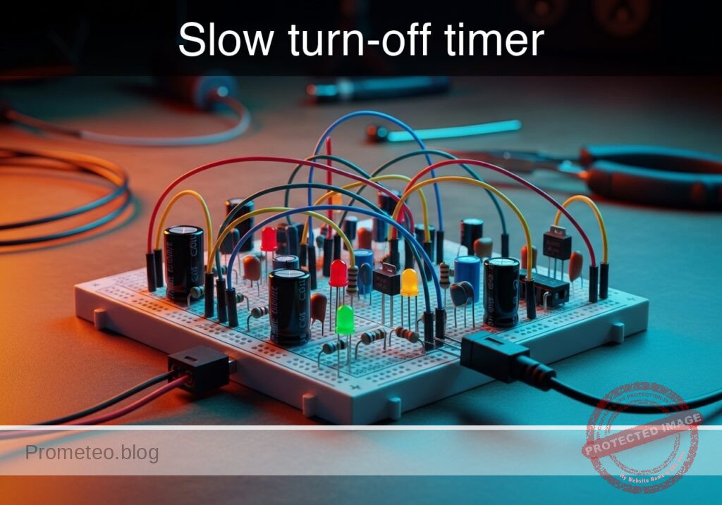
Slow turn-off timer prototype (Maker Style)

Level: Basic — Construct a circuit that fades an LED out slowly using capacitor discharge.

Objective and use case

In this practical case, you will build an analog timer circuit using an NPN transistor and a capacitor. When a push button is released, the LED will not turn off immediately; instead, it will dim gradually until it extinguishes.

  • Interior car lighting: mimics the effect of dome lights fading out after the door is closed.
  • Safety lighting: provides temporary illumination in hallways or stairwells after a switch is turned off.
  • Debouncing simulation: demonstrates how capacitors smooth out sudden signal changes.
  • Visualizing RC time constants: allows direct observation of electrical charge storage and decay.

Expected outcome:
* Immediate ON: When the button is pressed, the LED lights up instantly at full brightness.
* Delayed OFF: Upon releasing the button, the LED remains lit and fades out over a period of 2 to 5 seconds.
* Voltage Decay: If measured with a multimeter, the voltage at the capacitor decreases exponentially.
* Visual Feedback: The LED brightness directly correlates to the remaining charge in the capacitor.
* Target audience: Students and hobbyists understanding the relationship between capacitors and transistors.

Materials

  • V1: 9 V DC supply, function: main power source
  • S1: Momentary push button (Normally Open), function: trigger mechanism
  • R1: 100 Ω resistor, function: switch current protection (limits inrush current to capacitor)
  • R2: 22 kΩ resistor, function: base current limiting and timing control
  • R3: 470 Ω resistor, function: LED current limiting
  • C1: 1000 µF electrolytic capacitor, function: charge storage (timing tank)
  • Q1: 2N2222 (or BC547) NPN transistor, function: current switch/amplifier
  • D1: Red LED, function: visual output indicator

Wiring guide

Use the following node connections to assemble the circuit on a breadboard.

  • Power Nodes:

    • VCC: Positive rail (9 V).
    • 0: Ground rail (0 V).
  • Switch and Capacitor Network (Nodes: VCC, V_STORE, 0):

    • S1 connects between VCC and an intermediate node (internal to switch assembly).
    • R1 connects between the switch output and V_STORE. (When S1 is pressed, V_STORE charges to ~9 V).
    • C1 connects between V_STORE (positive leg) and 0 (negative leg).
  • Transistor Control (Nodes: V_STORE, V_BASE, 0):

    • R2 connects between V_STORE and V_BASE.
    • Q1 (Base) connects to V_BASE.
    • Q1 (Emitter) connects to 0.
  • Output Stage (Nodes: VCC, V_COLL):

    • R3 connects between VCC and the anode of D1.
    • D1 (Cathode) connects to V_COLL.
    • Q1 (Collector) connects to V_COLL.

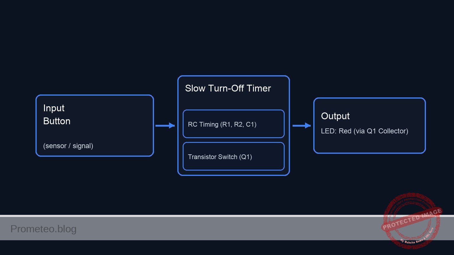
Conceptual block diagram

Conceptual block diagram — Slow Turn-Off Timer
Quick read: inputs → main block → output (actuator or measurement). This summarizes the ASCII schematic below.

Schematic

+-------------------------------------------------------------------------+
|                       SLOW TURN-OFF TIMER DIAGRAM                       |
+-------------------------------------------------------------------------+

1. TIMING & CONTROL LOOP (Charges C1, drives Transistor Base)
---------------------------------------------------------------------------

VCC (9 V) --> [ S1: Button ] --> [ R1: 100 ] --(V_STORE)--> [ R2: 22k ] --> [ Q1:Base ]
                                                  |
                                                  v
                                            [ C1: 1000u ]
                                                  |
                                                  v
                                                 GND


2. OUTPUT LOAD LOOP (Powering the LED)
---------------------------------------------------------------------------

VCC (9 V) --> [ R3: 470 ] --> [ LED: Red ] --> [ Q1:Collector ]
                                                     |
                                                     v
                                              (Current Flow)
                                                     v
                                              [ Q1:Emitter ] --> GND
Schematic (ASCII)

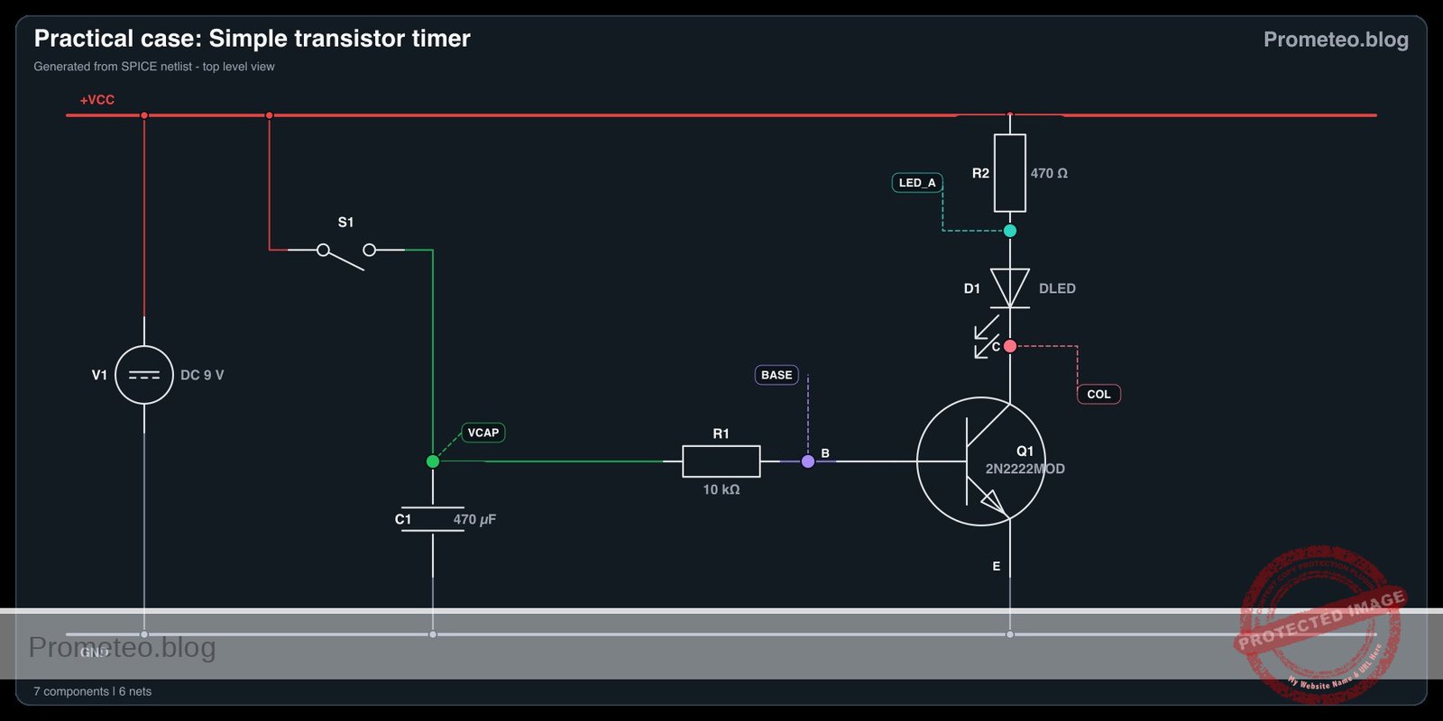
Electrical diagram

Electrical diagram for case: Simple transistor timer
Generated from the validated SPICE netlist for this case.

🔒 This electrical diagram is premium. With the monthly membership (7-day free trial) you can unlock the complete didactic material and the print-ready PDF pack.🔓 See premium access plans

Measurements and tests

To validate the circuit operation, perform the following steps:

  1. Charging phase: Press and hold S1. Measure the voltage at V_STORE relative to Ground. It should rise rapidly to approximately 9 V. The LED D1 should be fully lit.
  2. Base activation: While holding S1, measure the voltage at V_BASE. It should differ from V_STORE due to the drop across R2, stabilizing around 0.7 V – 0.8 V (the Base-Emitter saturation voltage).
  3. Discharge phase: Release S1. Observe D1. It should not turn off instantly. Instead, it should fade.
  4. Time measurement: Use a stopwatch to measure the time from the moment S1 is released until the LED is completely dark. With a 1000 µF capacitor and 22 kΩ resistor, this should take several seconds.
  5. Voltage tracking: Connect a multimeter to V_STORE immediately after releasing the button. Watch the voltage drop. The LED usually turns off when V_STORE drops below the threshold required to maintain sufficient base current through R2 (roughly when V_STORE approaches 1.5 V – 2 V).

SPICE netlist and simulation

Reference SPICE Netlist (ngspice) — excerptFull SPICE netlist (ngspice)

* Practical case: Slow turn-off timer
.width out=256

* --- Models ---
* Standard NPN Transistor Model
.model 2N2222 NPN(IS=1E-14 VAF=100 BF=200 IKF=0.3 XTB=1.5 BR=3 CJC=8E-12 CJE=25E-12 TR=46.91E-9 TF=411.1E-12 ITF=0.6 VTF=1.7 XTF=3 RB=10 RC=1 RE=1)
* Generic Red LED Model (Vf approx 1.8V-2V)
.model DLED D(IS=1e-22 RS=10 N=1.5 CJO=50p)
* Switch Model for Push Button
.model SW_BTN SW(Vt=2.5 Ron=0.1 Roff=100M)

* --- Power Supply ---
V1 VCC 0 DC 9

* --- Input / Trigger Mechanism ---
* S1: Push Button. Modeled as a voltage-controlled switch connecting VCC to SW_OUT.
* V_BTN_ACT: Simulates the user pressing the button. 
* Pulse starts at 1s, holds for 2s (simulating a solid press), then releases.
V_BTN_ACT CTRL 0 PULSE(0 5 1 0.1 0.1 2 100)
S1 VCC SW_OUT CTRL 0 SW_BTN
* ... (truncated in public view) ...

Copy this content into a .cir file and run with ngspice.

🔒 Part of this section is premium. With the monthly membership (7-day free trial) you can access the full content (materials, wiring, detailed build, validation, troubleshooting, variants and checklist) and download the complete print-ready PDF pack.

* Practical case: Slow turn-off timer
.width out=256

* --- Models ---
* Standard NPN Transistor Model
.model 2N2222 NPN(IS=1E-14 VAF=100 BF=200 IKF=0.3 XTB=1.5 BR=3 CJC=8E-12 CJE=25E-12 TR=46.91E-9 TF=411.1E-12 ITF=0.6 VTF=1.7 XTF=3 RB=10 RC=1 RE=1)
* Generic Red LED Model (Vf approx 1.8V-2V)
.model DLED D(IS=1e-22 RS=10 N=1.5 CJO=50p)
* Switch Model for Push Button
.model SW_BTN SW(Vt=2.5 Ron=0.1 Roff=100M)

* --- Power Supply ---
V1 VCC 0 DC 9

* --- Input / Trigger Mechanism ---
* S1: Push Button. Modeled as a voltage-controlled switch connecting VCC to SW_OUT.
* V_BTN_ACT: Simulates the user pressing the button. 
* Pulse starts at 1s, holds for 2s (simulating a solid press), then releases.
V_BTN_ACT CTRL 0 PULSE(0 5 1 0.1 0.1 2 100)
S1 VCC SW_OUT CTRL 0 SW_BTN

* --- Switch Current Protection & Charging ---
* R1 limits inrush current to C1 when S1 is closed.
R1 SW_OUT V_STORE 100

* --- Timing Tank ---
* C1 charges when S1 is closed and discharges through R2/Q1 when open.
C1 V_STORE 0 1000u

* --- Transistor Control ---
* R2 provides base current and sets the discharge timing constant (Tau = R2*C1 approx 22s).
R2 V_STORE V_BASE 22k

* --- Transistor Switch ---
* Q1 NPN Transistor (2N2222)
* Collector: V_COLL, Base: V_BASE, Emitter: 0 (GND)
Q1 V_COLL V_BASE 0 2N2222

* --- Output Stage ---
* R3 limits current through the LED.
R3 VCC LED_ANODE 470
* D1 Red LED. Anode at LED_ANODE, Cathode at V_COLL.
D1 LED_ANODE V_COLL DLED

* --- Simulation Commands ---
.op
* Transient analysis for 60 seconds to capture the slow decay (RC ~ 22s).
.tran 0.1s 60s

* --- Output Directives ---
* Printing Capacitor Voltage (Timing) and Collector Voltage (Output State)
.print tran V(V_STORE) V(V_COLL) V(LED_ANODE) V(SW_OUT)

Simulation Results (Transient Analysis)

Simulation Results (Transient Analysis)
Show raw data table (640 rows)
Index   time            v(v_store)      v(v_coll)       v(led_anode)    v(sw_out)
0	0.000000e+00	8.962619e+00	1.066236e-01	2.056192e+00	8.999963e+00
1	1.000000e-03	8.962619e+00	1.066236e-01	2.056192e+00	8.999963e+00
2	2.000000e-03	8.962619e+00	1.066236e-01	2.056192e+00	8.999963e+00
3	4.000000e-03	8.962619e+00	1.066236e-01	2.056192e+00	8.999963e+00
4	8.000000e-03	8.962619e+00	1.066236e-01	2.056192e+00	8.999963e+00
5	1.600000e-02	8.962619e+00	1.066236e-01	2.056192e+00	8.999963e+00
6	3.200000e-02	8.962619e+00	1.066236e-01	2.056192e+00	8.999963e+00
7	6.400000e-02	8.962619e+00	1.066236e-01	2.056192e+00	8.999963e+00
8	1.280000e-01	8.962619e+00	1.066236e-01	2.056192e+00	8.999963e+00
9	2.280000e-01	8.962619e+00	1.066236e-01	2.056192e+00	8.999963e+00
10	3.280000e-01	8.962619e+00	1.066236e-01	2.056192e+00	8.999963e+00
11	4.280000e-01	8.962619e+00	1.066236e-01	2.056192e+00	8.999963e+00
12	5.280000e-01	8.962619e+00	1.066236e-01	2.056192e+00	8.999963e+00
13	6.280000e-01	8.962619e+00	1.066236e-01	2.056192e+00	8.999963e+00
14	7.280000e-01	8.962619e+00	1.066236e-01	2.056192e+00	8.999963e+00
15	8.280000e-01	8.962619e+00	1.066236e-01	2.056192e+00	8.999963e+00
16	9.280000e-01	8.962619e+00	1.066236e-01	2.056192e+00	8.999963e+00
17	1.000000e+00	8.962619e+00	1.066236e-01	2.056192e+00	8.999963e+00
18	1.010000e+00	8.962619e+00	1.066236e-01	2.056192e+00	8.999963e+00
19	1.026000e+00	8.962619e+00	1.066236e-01	2.056192e+00	8.999963e+00
20	1.030750e+00	8.962619e+00	1.066236e-01	2.056192e+00	8.999963e+00
21	1.039062e+00	8.962619e+00	1.066236e-01	2.056192e+00	8.999963e+00
22	1.041363e+00	8.962619e+00	1.066236e-01	2.056192e+00	8.999963e+00
23	1.045390e+00	8.962619e+00	1.066236e-01	2.056192e+00	8.999963e+00
... (616 more rows) ...


Reference SPICE netlist (ngspice)

* Practical case: Slow turn-off timer
.width out=256

* --- Models ---
* Standard NPN Transistor Model
.model 2N2222 NPN(IS=1E-14 VAF=100 BF=200 IKF=0.3 XTB=1.5 BR=3 CJC=8E-12 CJE=25E-12 TR=46.91E-9 TF=411.1E-12 ITF=0.6 VTF=1.7 XTF=3 RB=10 RC=1 RE=1)
* Generic Red LED Model (Vf approx 1.8V-2V)
.model DLED D(IS=1e-22 RS=10 N=1.5 CJO=50p)
* Switch Model for Push Button
.model SW_BTN SW(Vt=2.5 Ron=0.1 Roff=100M)

* --- Power Supply ---
V1 VCC 0 DC 9

* --- Input / Trigger Mechanism ---
* S1: Push Button. Modeled as a voltage-controlled switch connecting VCC to SW_OUT.
* V_BTN_ACT: Simulates the user pressing the button.
* Pulse starts at 1s, holds for 2s (simulating a solid press), then releases.
V_BTN_ACT CTRL 0 PULSE(0 5 1 0.1 0.1 2 100)
S1 VCC SW_OUT CTRL 0 SW_BTN

* --- Switch Current Protection & Charging ---
* R1 limits inrush current to C1 when S1 is closed.
R1 SW_OUT V_STORE 100

* --- Timing Tank ---
* C1 charges when S1 is closed and discharges through R2/Q1 when open.
C1 V_STORE 0 1000u

* --- Transistor Control ---
* R2 provides base current and sets the discharge timing constant (Tau = R2*C1 approx 22s).
R2 V_STORE V_BASE 22k

* --- Transistor Switch ---
* Q1 NPN Transistor (2N2222)
* Collector: V_COLL, Base: V_BASE, Emitter: 0 (GND)
Q1 V_COLL V_BASE 0 2N2222

* --- Output Stage ---
* R3 limits current through the LED.
R3 VCC LED_ANODE 470
* D1 Red LED. Anode at LED_ANODE, Cathode at V_COLL.
D1 LED_ANODE V_COLL DLED

* --- Simulation Commands ---
.op
* Transient analysis for 60 seconds to capture the slow decay (RC ~ 22s).
.tran 0.1s 60s

* --- Output Directives ---
* Printing Capacitor Voltage (Timing) and Collector Voltage (Output State)
.print tran V(V_STORE) V(V_COLL) V(LED_ANODE) V(SW_OUT)

Simulation Results (Transient Analysis)

Simulation Results (Transient Analysis)

Common mistakes and how to avoid them

  1. Capacitor polarity reversed: Electrolytic capacitors have a specific polarity. Connecting the negative stripe to the positive voltage can cause the component to heat up or pop. Solution: Ensure the leg marked with a stripe (negative) connects to Ground.
  2. R2 value too low: If R2 is very small (e.g., 1 kΩ), the capacitor will discharge into the transistor base very quickly, resulting in no visible fading effect. Solution: Use a high resistance value (10 kΩ–47 kΩ) to slow down the discharge.
  3. Omitting R1: Connecting the switch directly to a large capacitor creates a massive current spike (spark) when pressed. Solution: Always use a small resistor (100 Ω) in series with the switch to protect the contacts.

Troubleshooting

  • LED turns off instantly (no fade):
    • Cause: Capacitor C1 is missing, disconnected, or the value is too small (e.g., 100 nF instead of 1000 µF).
    • Fix: Verify C1 is correctly seated and is at least 470 µF.
  • LED stays on permanently:
    • Cause: The switch S1 might be the wrong type (Latching instead of Momentary) or there is a short circuit bypassing the transistor.
    • Fix: Ensure the button releases physically and check wiring around the Collector-Emitter.
  • LED is very dim even when button is pressed:
    • Cause: R2 (Base resistor) is too high (limiting base current too much) or R3 (LED resistor) is too high.
    • Fix: Check that R2 is roughly 22 kΩ and R3 is roughly 470 Ω.

Possible improvements and extensions

  1. Variable Timing: Replace R2 with a 100 kΩ potentiometer in series with a 1 kΩ resistor. This allows you to adjust the fade-out duration manually.
  2. Darlington Pair: Replace Q1 with a Darlington transistor (or two NPNs connected in Darlington configuration). This offers a much higher current gain, allowing you to use a much larger R2 (e.g., 1 MΩ), resulting in extremely long timer durations (minutes) with the same capacitor.

More Practical Cases on Prometeo.blog

Find this product and/or books on this topic on Amazon

Go to Amazon

As an Amazon Associate, I earn from qualifying purchases. If you buy through this link, you help keep this project running.

Quick Quiz

Question 1: What is the primary function of the circuit described in the text?


Question 2: Which component is responsible for storing the electrical charge that keeps the LED lit after the button is released?


Question 3: What real-world application mimics the effect created by this circuit?


Question 4: What happens to the LED immediately when the push button is pressed?


Question 5: Based on the text, what is the purpose of the resistor R1 (100 Ω) in this specific circuit design?


Question 6: Which type of transistor is specified for use in this project?


Question 7: If you measure the voltage at the capacitor after releasing the button, how does it behave?


Question 8: What is the expected duration for the LED to fade out after releasing the button?


Question 9: Besides lighting, what concept does this circuit demonstrate regarding signal changes?


Question 10: What physical phenomenon allows the direct observation of electrical charge storage and decay in this project?


Carlos Núñez Zorrilla
Electronics & Computer Engineer

Telecommunications Electronics Engineer and Computer Engineer (official degrees in Spain).
Follow me:


Practical case: Simple audio amplifier

Simple audio amplifier prototype (Maker Style)

Level: Basic. Build a circuit to amplify a weak audio signal using an NPN transistor in common-emitter configuration.

Objective and use case

In this case, you will build a classic single-stage Class A amplifier using an NPN transistor with voltage divider biasing. You will input a small AC signal (representing audio) and observe a larger voltage swing at the output.

  • Why it is useful:

    • Pre-amplification: Boosts weak signals from microphones before they reach a power amplifier.
    • Signal conditioning: Raises sensor output levels to be readable by microcontrollers.
    • Analog processing: Fundamental building block for filters, oscillators, and mixers.
    • Impedance matching: Buffers high-impedance sources to drive lower-impedance loads (depending on specific configuration).
  • Expected outcome:

    • DC Operating Point: VCE stabilizes around half the supply voltage (VCC / 2) for maximum swing.
    • Amplification: The AC output voltage (Vout) is significantly larger than the input (Vin), indicating Voltage Gain (Av > 1).
    • Phase Inversion: The output signal waveform is inverted (180^\circ) relative to the input.
    • Current Flow: IC is controlled by IB according to the transistor’s beta (\beta).
  • Target audience and level: Students with basic knowledge of Ohm’s Law and component identification.

Materials

  • V1: 9 V DC battery or bench supply, function: main circuit power.
  • V2: Signal Generator (Sine wave, 1 kHz, 20 mV peak-to-peak), function: simulates weak audio input.
  • Q1: 2N3904 (or 2N2222) NPN BJT, function: active amplifying element.
  • R1: 22 kΩ resistor, function: upper base bias divider.
  • R2: 6.8 kΩ resistor, function: lower base bias divider.
  • R3: 4.7 kΩ resistor, function: collector load (sets gain and output impedance).
  • R4: 1 kΩ resistor, function: emitter degeneration (sets DC stability).
  • C1: 10 µF electrolytic capacitor, function: input DC blocking.
  • C2: 10 µF electrolytic capacitor, function: output DC blocking.
  • C3: 100 µF electrolytic capacitor, function: emitter bypass (increases AC gain).

Wiring guide

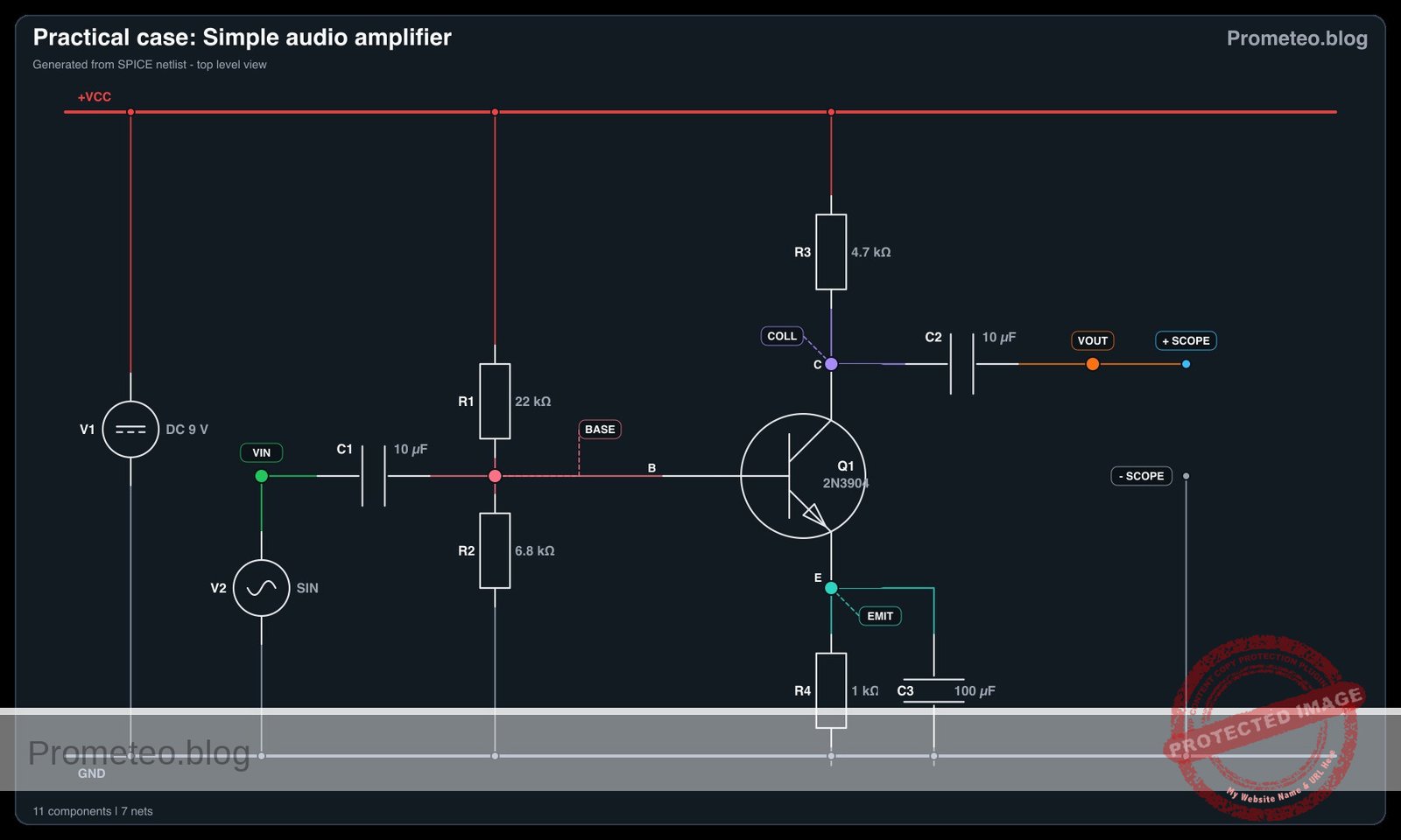
Use the following nodes to wire your circuit: VCC (9 V), 0 (GND), BASE, COLL, EMIT, VIN, VOUT.

  • V1: Positive terminal connects to VCC, Negative terminal connects to 0.
  • V2: Signal output connects to VIN, Ground connects to 0.
  • R1: Connects between VCC and BASE.
  • R2: Connects between BASE and 0.
  • R3: Connects between VCC and COLL.
  • R4: Connects between EMIT and 0.
  • Q1: Collector pin to COLL, Base pin to BASE, Emitter pin to EMIT.
  • C1: Positive leg to BASE, Negative leg to VIN.
  • C2: Positive leg to COLL, Negative leg to VOUT (Load/Scope probe connects here).
  • C3: Positive leg to EMIT, Negative leg to 0 (Place in parallel with R4).

Conceptual block diagram

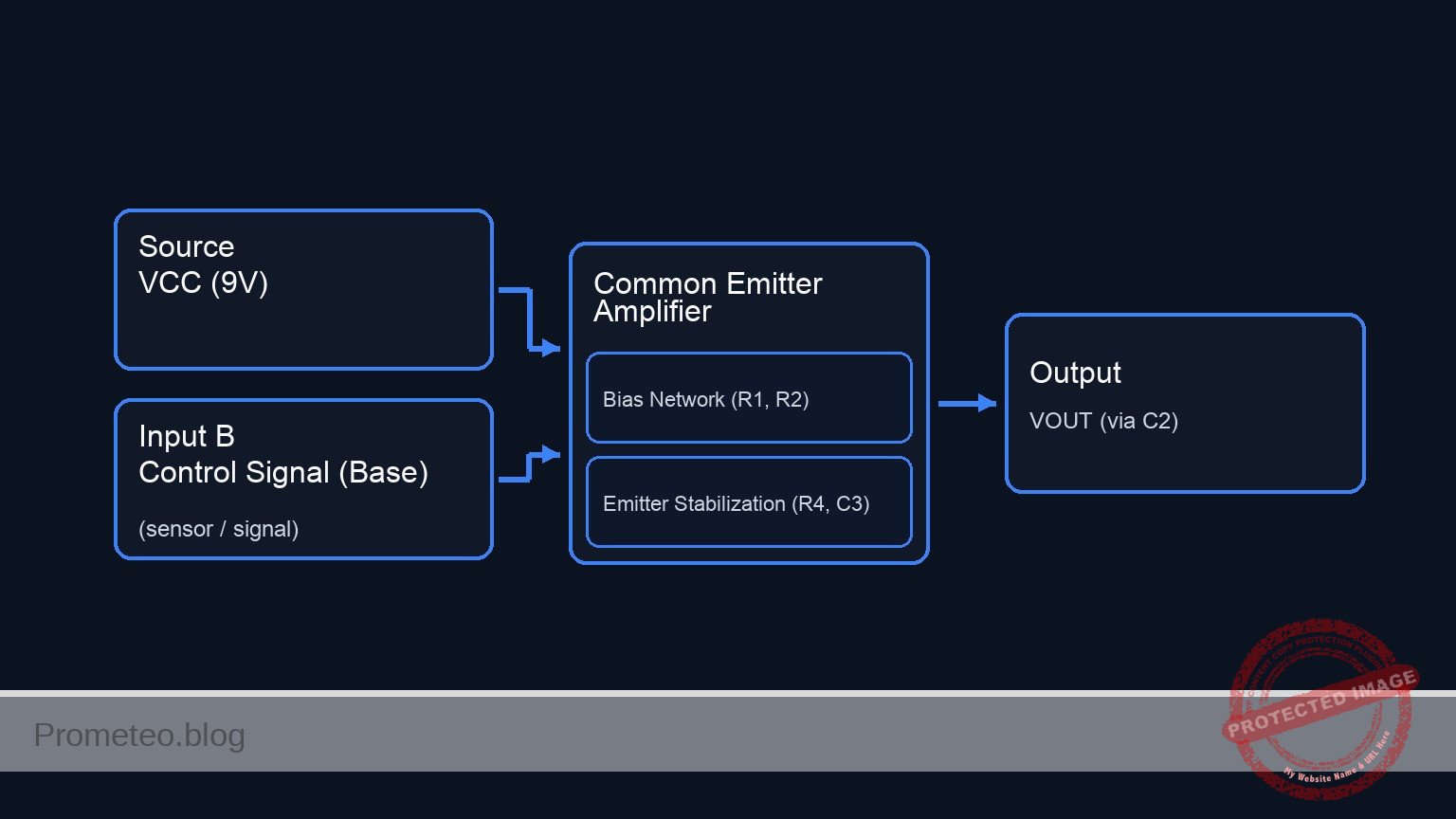
Conceptual block diagram — Common Emitter Amplifier
Quick read: inputs → main block → output (actuator or measurement). This summarizes the ASCII schematic below.

Schematic

Title: Practical case: Simple audio amplifier

      (BIAS & INPUT NETWORK)                               (POWER & OUTPUT NETWORK)
      ======================                               ========================

                                                           VCC (9 V)
      VCC (9 V)                                                |
         |                                                    |
         v                                                    v
    [ R1: 22k ]                                          [ R3: 4.7k ]
         |                                                    |
         v                                                    v
      (BASE) --------(Control Signal)----------------> [ Q1: Collector ] <--(COLL)--+
         ^                                                    |                     |
         |                                                    | (Amplified Current) |
    [ C1: 10uF ] <--(VIN)-- [ V2: Source ]                    v                     |
         |                                             [ Q1: Emitter ]              +--> [ C2: 10uF ] --> VOUT
         v                                                    |
    [ R2: 6.8k ]                                              v
         |                                                  (EMIT)
         v                                                    |
        GND                                       +-----------+-----------+
                                                  |                       |
                                                  v                       v
                                             [ R4: 1k ]             [ C3: 100uF ]
                                                  |                       |
                                                  v                       v
                                                 GND                     GND
Schematic (ASCII)

Electrical diagram

Electrical diagram for case: Simple audio amplifier
Generated from the validated SPICE netlist for this case.

🔒 This electrical diagram is premium. With the monthly membership (7-day free trial) you can unlock the complete didactic material and the print-ready PDF pack.🔓 See premium access plans

Measurements and tests

Perform these tests using a Multimeter (DMM) and an Oscilloscope (if available).

  1. DC Bias Check (Quiescent Point):

    • Ensure V2 (AC source) is OFF or disconnected.
    • Measure voltage from COLL to 0. It should be approximately 4 V to 5 V (roughly half of VCC).
    • Measure voltage from EMIT to 0. It should be approximately 1 V (VE).
    • Measure voltage from BASE to EMIT (VBE). It must be ~0.65 V to 0.7 V for the transistor to be active.
  2. Current Calculation:

    • Calculate Collector Current (IC): IC ≈ VEMIT / R4. Expect approx 1 mA.
    • Calculate Base Current (IB): IC / \beta (assuming \beta ≈ 100, IB ≈ 10 µ A).
  3. AC Gain Verification:

    • Connect V2 (VIN) with a 20 mV peak-to-peak sine wave at 1 kHz.
    • Measure the Peak-to-Peak voltage at VOUT.
    • Calculate Voltage Gain (Av): Av = Voutpp / Vinpp.
    • Observation: Without C3, gain is low (≈ R3 / R4). With C3 connected, gain should increase significantly.

SPICE netlist and simulation

Reference SPICE Netlist (ngspice) — excerptFull SPICE netlist (ngspice)

* Practical case: Simple audio amplifier

* --- Power Supply ---
* V1: 9 V DC battery
V1 VCC 0 DC 9

* --- Input Signal ---
* V2: Signal Generator (Sine wave, 1 kHz, 20 mV peak-to-peak -> 10mV Amplitude)
V2 VIN 0 SIN(0 10m 1k)

* --- Components ---
* Q1: 2N3904 NPN BJT
Q1 COLL BASE EMIT 2N3904

* R1: Upper base bias divider
R1 VCC BASE 22k

* R2: Lower base bias divider
R2 BASE 0 6.8k

* ... (truncated in public view) ...

Copy this content into a .cir file and run with ngspice.

🔒 Part of this section is premium. With the monthly membership (7-day free trial) you can access the full content (materials, wiring, detailed build, validation, troubleshooting, variants and checklist) and download the complete print-ready PDF pack.

* Practical case: Simple audio amplifier

* --- Power Supply ---
* V1: 9 V DC battery
V1 VCC 0 DC 9

* --- Input Signal ---
* V2: Signal Generator (Sine wave, 1 kHz, 20 mV peak-to-peak -> 10mV Amplitude)
V2 VIN 0 SIN(0 10m 1k)

* --- Components ---
* Q1: 2N3904 NPN BJT
Q1 COLL BASE EMIT 2N3904

* R1: Upper base bias divider
R1 VCC BASE 22k

* R2: Lower base bias divider
R2 BASE 0 6.8k

* R3: Collector load
R3 VCC COLL 4.7k

* R4: Emitter degeneration
R4 EMIT 0 1k

* C1: Input DC blocking (Positive leg to BASE, Negative leg to VIN)
C1 BASE VIN 10u

* C2: Output DC blocking (Positive leg to COLL, Negative leg to VOUT)
C2 COLL VOUT 10u

* C3: Emitter bypass (Positive leg to EMIT, Negative leg to 0)
C3 EMIT 0 100u

* --- Load Simulation ---
* High impedance load to simulate scope probe and prevent floating node error at VOUT
R_SCOPE VOUT 0 1Meg

* --- Models ---
.model 2N3904 NPN(IS=1E-14 VAF=100 BF=300 IKF=0.4 XTB=1.5 BR=4 CJC=4E-12 CJE=8E-12 RB=20 RC=0.1 RE=0.1 TR=250n TF=350p ITF=1 VTF=2 XTF=3)

* --- Analysis Directives ---
.op
.tran 10u 5ms

* --- Output ---
* Prints Input and Output voltages, plus internal transistor nodes
.print tran V(VIN) V(VOUT) V(BASE) V(COLL) V(EMIT)

.end

Simulation Results (Transient Analysis)

Simulation Results (Transient Analysis)
Show raw data table (511 rows)
Index   time            v(vin)          v(vout)         v(base)         v(coll)         v(emit)
0	0.000000e+00	0.000000e+00	0.000000e+00	2.100182e+00	2.275541e+00	1.435514e+00
1	1.000000e-07	6.283185e-06	-1.11372e-03	2.100188e+00	2.274427e+00	1.435514e+00
2	2.000000e-07	1.256637e-05	-2.51792e-03	2.100195e+00	2.273023e+00	1.435514e+00
3	4.000000e-07	2.513271e-05	-5.47602e-03	2.100207e+00	2.270065e+00	1.435514e+00
4	8.000000e-07	5.026527e-05	-1.15278e-02	2.100232e+00	2.264013e+00	1.435514e+00
5	1.600000e-06	1.005293e-04	-2.35622e-02	2.100283e+00	2.251979e+00	1.435514e+00
6	3.200000e-06	2.010484e-04	-4.77358e-02	2.100383e+00	2.227805e+00	1.435514e+00
7	6.400000e-06	4.020155e-04	-9.61836e-02	2.100584e+00	2.179357e+00	1.435514e+00
8	1.280000e-05	8.033810e-04	-1.93689e-01	2.100985e+00	2.081852e+00	1.435516e+00
9	2.280000e-05	1.427671e-03	-3.47124e-01	2.101609e+00	1.928416e+00	1.435522e+00
10	3.280000e-05	2.046327e-03	-5.01331e-01	2.102227e+00	1.774210e+00	1.435531e+00
11	4.280000e-05	2.656907e-03	-6.48595e-01	2.102836e+00	1.626945e+00	1.435544e+00
12	5.280000e-05	3.257002e-03	-7.15494e-01	2.103433e+00	1.560045e+00	1.435558e+00
13	6.280000e-05	3.844242e-03	-7.38189e-01	2.104013e+00	1.537349e+00	1.435575e+00
14	7.280000e-05	4.416311e-03	-7.50146e-01	2.104572e+00	1.525391e+00	1.435592e+00
15	8.280000e-05	4.970951e-03	-7.58389e-01	2.105109e+00	1.517147e+00	1.435610e+00
16	9.280000e-05	5.505973e-03	-7.63991e-01	2.105621e+00	1.511545e+00	1.435628e+00
17	1.028000e-04	6.019265e-03	-7.68326e-01	2.106106e+00	1.507209e+00	1.435647e+00
18	1.128000e-04	6.508802e-03	-7.71816e-01	2.106563e+00	1.503719e+00	1.435667e+00
19	1.228000e-04	6.972652e-03	-7.74681e-01	2.106990e+00	1.500853e+00	1.435687e+00
20	1.328000e-04	7.408984e-03	-7.77018e-01	2.107384e+00	1.498515e+00	1.435707e+00
21	1.428000e-04	7.816076e-03	-7.78966e-01	2.107746e+00	1.496566e+00	1.435728e+00
22	1.528000e-04	8.192321e-03	-7.80567e-01	2.108073e+00	1.494964e+00	1.435750e+00
23	1.628000e-04	8.536235e-03	-7.81896e-01	2.108365e+00	1.493635e+00	1.435772e+00
... (487 more rows) ...


Reference SPICE netlist (ngspice)

* Practical case: Simple audio amplifier

* --- Power Supply ---
* V1: 9 V DC battery
V1 VCC 0 DC 9

* --- Input Signal ---
* V2: Signal Generator (Sine wave, 1 kHz, 20 mV peak-to-peak -> 10mV Amplitude)
V2 VIN 0 SIN(0 10m 1k)

* --- Components ---
* Q1: 2N3904 NPN BJT
Q1 COLL BASE EMIT 2N3904

* R1: Upper base bias divider
R1 VCC BASE 22k

* R2: Lower base bias divider
R2 BASE 0 6.8k

* R3: Collector load
R3 VCC COLL 4.7k

* R4: Emitter degeneration
R4 EMIT 0 1k

* C1: Input DC blocking (Positive leg to BASE, Negative leg to VIN)
C1 BASE VIN 10u

* C2: Output DC blocking (Positive leg to COLL, Negative leg to VOUT)
C2 COLL VOUT 10u

* C3: Emitter bypass (Positive leg to EMIT, Negative leg to 0)
C3 EMIT 0 100u

* --- Load Simulation ---
* High impedance load to simulate scope probe and prevent floating node error at VOUT
R_SCOPE VOUT 0 1Meg

* --- Models ---
.model 2N3904 NPN(IS=1E-14 VAF=100 BF=300 IKF=0.4 XTB=1.5 BR=4 CJC=4E-12 CJE=8E-12 RB=20 RC=0.1 RE=0.1 TR=250n TF=350p ITF=1 VTF=2 XTF=3)

* --- Analysis Directives ---
.op
.tran 10u 5ms

* --- Output ---
* Prints Input and Output voltages, plus internal transistor nodes
.print tran V(VIN) V(VOUT) V(BASE) V(COLL) V(EMIT)

.end

Simulation Results (Transient Analysis)

Simulation Results (Transient Analysis)

Common mistakes and how to avoid them

  1. Transistor Pinout Reversal: Swapping the Collector and Emitter prevents amplification and acts like a reverse-biased diode.
    • Solution: Double-check the datasheet for the 2N3904 (E-B-C flat side facing you) before inserting.
  2. Capacitor Polarity: Electrolytic capacitors (C1, C2, C3) explode or fail if biased backwards.
    • Solution: Ensure the positive lead (longer leg) faces the more positive DC potential (towards the transistor base/collector).
  3. Saturation or Cutoff: Using wrong resistor values shifts the Q-point, causing the signal to clip (flatten) immediately.
    • Solution: Verify DC voltages at the Collector before applying an AC signal. If VC is near 9 V or 0 V, check R1 and R2.

Troubleshooting

  • Symptom: No Output Signal.
    • Cause: Loose connection, blown transistor, or V1 is off.
    • Fix: Check continuity on the breadboard rails; verify V1 is 9 V.
  • Symptom: Output is Clipped (Flat tops or bottoms).
    • Cause: The amplifier is driven into saturation (flat bottom) or cutoff (flat top), or input signal is too large.
    • Fix: Reduce input amplitude (V2); check bias resistors (R1, R2) to center the Q-point.
  • Symptom: Low Gain (Output ≈ Input).
    • Cause: Bypass capacitor C3 is missing, loose, or too small.
    • Fix: Ensure C3 is connected solidly in parallel with R4. This shorts the emitter resistor for AC signals, maximizing gain.

Possible improvements and extensions

  1. Volume Control: Replace R2 (or add a pot before C1) with a 10 kΩ potentiometer to attenuate the input signal.
  2. Increased Power: Add a second transistor stage (Emitter Follower / Class B push-pull) after VOUT to drive a small 8 Ω speaker instead of just observing voltage on a scope.

More Practical Cases on Prometeo.blog

Find this product and/or books on this topic on Amazon

Go to Amazon

As an Amazon Associate, I earn from qualifying purchases. If you buy through this link, you help keep this project running.

Quick Quiz

Question 1: What is the primary objective of the circuit described in the text?


Question 2: Which transistor configuration is used in this amplifier circuit?


Question 3: What is the expected phase relationship between the input and output signals in this configuration?


Question 4: Ideally, where should the DC operating point (V_CE) stabilize for maximum voltage swing?


Question 5: Which component serves as the active amplifying element in this circuit?


Question 6: What is the purpose of the signal generator (V2) in this setup?


Question 7: Which of the following is explicitly listed as a use case for this type of amplifier?


Question 8: What does a Voltage Gain (Av > 1) signify in this context?


Question 9: What role does resistor R1 (22 kΩ) typically play in a voltage divider biasing network?


Question 10: According to standard BJT theory implied in the text, the collector current (I_C) is primarily controlled by the base current (I_B) and which parameter?


Carlos Núñez Zorrilla
Electronics & Computer Engineer

Telecommunications Electronics Engineer and Computer Engineer (official degrees in Spain).
Follow me:


Practical case: The transistor as a light switch

The transistor as a light switch prototype (Maker Style)

Level: Basic. Objective: Understand BJT cut-off and saturation to control a load (LED) with a small control signal.

Objective and use case

In this practical case, you will build a circuit using an NPN Bipolar Junction Transistor (BJT) to switch a high-current load (an LED) on and off using a low-current control signal triggered by a push button.

Why it is useful:
* Microcontroller interfacing: Allows low-power pins (like those on an Arduino or ESP32) to drive higher current loads.
* Sensor actuation: Enables weak signals from sensors (like LDRs or thermistors) to activate lights or alarms.
* Component protection: Separates the sensitive control circuit from the power circuit.
* Logic switching: Forms the fundamental building block of digital logic gates.

Expected outcome:
* Idle State (Button Released): The transistor is in Cut-off. IC ≈ 0 mA, LED is OFF, and VCE ≈ Vsupply.
* Active State (Button Pressed): The transistor enters Saturation. LED is ON.
* Saturation Voltage: VCE drops to approximately $0.1$ V to $0.2$ V.
* Base Threshold: VBE stabilizes around $0.7$ V when the transistor is conducting.

Target audience: Basic level electronics students.

Materials

  • V1: 9 V DC battery or power supply, function: Main circuit power.
  • S1: Tactile Push-button (Normally Open), function: User input trigger.
  • R1: 10 kΩ resistor, function: Base current limiting (to ensure saturation without damaging the Base).
  • R2: 100 kΩ resistor, function: Pull-down resistor (keeps Base at 0 V when S1 is open).
  • R3: 330 Ω resistor, function: LED current limiting protection.
  • Q1: 2N2222 (or BC547) NPN Transistor, function: Electronic switch.
  • D1: Red LED, function: Visual load indicator.

Wiring guide

This guide uses specific node names to help you visualize the connections.
* Power Nodes: Connect V1 positive to node VCC and negative to node 0 (GND).
* Input Stage:
* Connect one side of S1 to VCC.
* Connect the other side of S1 to node INPUT_SIG.
* Connect R1 (10 kΩ) between INPUT_SIG and node BASE.
* Connect R2 (100 kΩ) between node BASE and node 0 (GND).
* Transistor Connections:
* Connect the Base of Q1 to node BASE.
* Connect the Emitter of Q1 directly to node 0 (GND).
* Connect the Collector of Q1 to node COLL.
* Output Load:
* Connect R3 (330 Ω) between VCC and node LED_ANODE.
* Connect the Anode (long leg) of D1 to node LED_ANODE.
* Connect the Cathode (short leg, flat side) of D1 to node COLL.

Conceptual block diagram

Conceptual block diagram — Transistor Switch (NPN)
Quick read: inputs → main block → output (actuator or measurement). This summarizes the ASCII schematic below.

Schematic

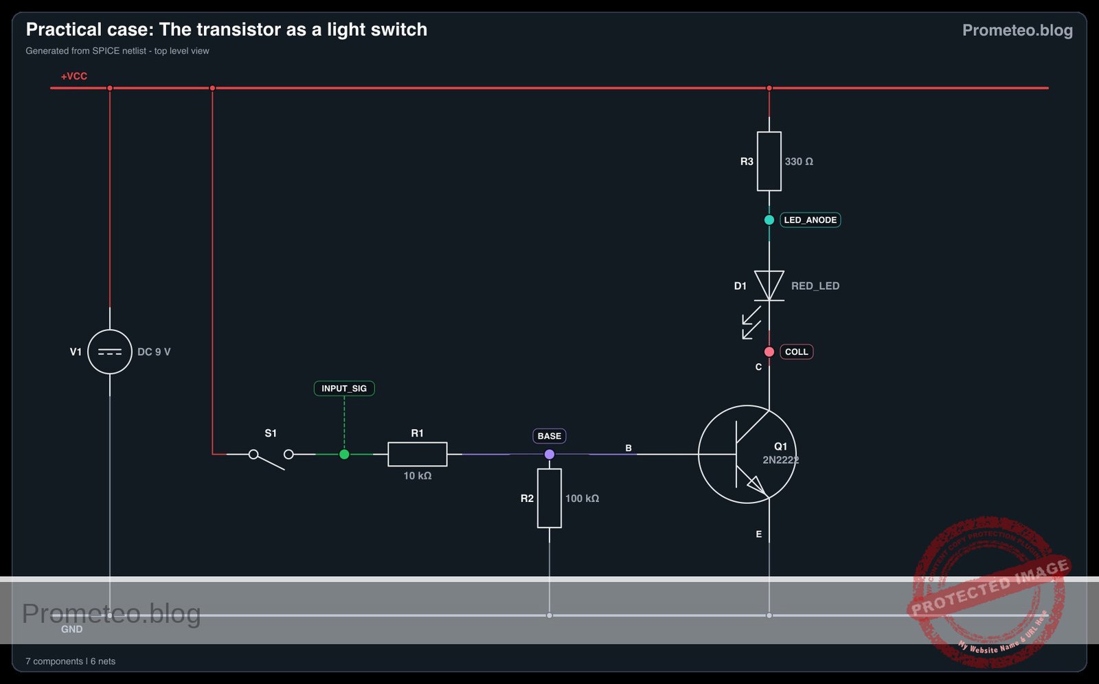
Title: Practical case: The transistor as a light switch

1. CONTROL PATH (Input Stage)
   Flow: VCC triggers the Base when S1 is pressed. R2 ensures Base is 0 V when S1 is open.

   [ VCC ] --> [ S1: Button ] --(INPUT_SIG)--> [ R1: 10k ] --(BASE)--+--> [ Q1: Base ]
                                                                     |
                                                                     +--> [ R2: 100k ] --> [ GND ]

2. LOAD PATH (Output Stage)
   Flow: Current flows from VCC through the LED into the Transistor Collector.

   [ VCC ] --> [ R3: 330R ] --(LED_ANODE)--> [ D1: Red LED ] --(COLL)--> [ Q1: Collector ]

3. COMMON RETURN (Grounding)
   Flow: The transistor completes the circuit to Ground.

   [ Q1: Emitter ] --> [ GND ]
Schematic (ASCII)

Electrical diagram

Electrical diagram for case: The transistor as a light switch
Generated from the validated SPICE netlist for this case.

🔒 This electrical diagram is premium. With the monthly membership (7-day free trial) you can unlock the complete didactic material and the print-ready PDF pack.🔓 See premium access plans

Measurements and tests

Perform these steps with a multimeter to verify the transistor regions of operation.

  1. Test Cut-off Region (Switch Open):

    • Ensure S1 is not pressed.
    • Measure voltage between Base and Emitter (VBE). Result should be 0 V.
    • Measure voltage between Collector and Emitter (VCE). Result should be close to 9 V (Source voltage), indicating the switch is open.
    • Observe D1: It must be OFF.
  2. Test Saturation Region (Switch Closed):

    • Press and hold S1.
    • Measure voltage between Base and Emitter (VBE). Result should be approximately 0.65 V to 0.75 V.
    • Measure voltage between Collector and Emitter (VCE). Result should drop to < 0.2 V. This voltage drop proves the transistor is acting as a closed switch (Saturation).
    • Observe D1: It must turn ON brightly.

SPICE netlist and simulation

Reference SPICE Netlist (ngspice) — excerptFull SPICE netlist (ngspice)

* Practical case: The transistor as a light switch
* Improved Netlist with robust switch modelling

.width out=256

* --- Power Supply ---
* V1: 9 V DC battery (Main circuit power)
V1 VCC 0 DC 9

* --- User Input Trigger (S1) ---
* S1: Tactile Push-button (Normally Open) connecting VCC to INPUT_SIG.
* Modeled using a Voltage-Controlled Switch (S1) driven by a control pulse (V_ACT).
* V_ACT simulates the user pressing the button (Logic 0 -> 1 -> 0).
V_ACT ACTUATE 0 PULSE(0 5 1ms 100u 100u 5ms 20ms)
S1 VCC INPUT_SIG ACTUATE 0 SW_TACTILE

* --- Input Stage ---
* R1: 10 kOhm, Base current limiting
R1 INPUT_SIG BASE 10k

* ... (truncated in public view) ...

Copy this content into a .cir file and run with ngspice.

🔒 Part of this section is premium. With the monthly membership (7-day free trial) you can access the full content (materials, wiring, detailed build, validation, troubleshooting, variants and checklist) and download the complete print-ready PDF pack.

* Practical case: The transistor as a light switch
* Improved Netlist with robust switch modelling

.width out=256

* --- Power Supply ---
* V1: 9 V DC battery (Main circuit power)
V1 VCC 0 DC 9

* --- User Input Trigger (S1) ---
* S1: Tactile Push-button (Normally Open) connecting VCC to INPUT_SIG.
* Modeled using a Voltage-Controlled Switch (S1) driven by a control pulse (V_ACT).
* V_ACT simulates the user pressing the button (Logic 0 -> 1 -> 0).
V_ACT ACTUATE 0 PULSE(0 5 1ms 100u 100u 5ms 20ms)
S1 VCC INPUT_SIG ACTUATE 0 SW_TACTILE

* --- Input Stage ---
* R1: 10 kOhm, Base current limiting
R1 INPUT_SIG BASE 10k

* R2: 100 kOhm, Pull-down resistor (keeps Base low when S1 is open)
R2 BASE 0 100k

* --- Transistor Switch ---
* Q1: 2N2222 NPN Transistor
* Connections: Collector=COLL, Base=BASE, Emitter=0(GND)
Q1 COLL BASE 0 2N2222

* --- Output Load ---
* R3: 330 Ohm, LED current limiting resistor
R3 VCC LED_ANODE 330

* D1: Red LED
* Connections: Anode=LED_ANODE, Cathode=COLL
D1 LED_ANODE COLL RED_LED

* --- Component Models ---
* Switch Model: Added hysteresis (Vh) and relaxed Ron for better convergence
.model SW_TACTILE SW(Vt=2.5 Vh=0.1 Ron=1 Roff=100Meg)

* Transistor Model: Standard 2N2222 parameters
.model 2N2222 NPN(IS=1E-14 VAF=100 BF=200 IKF=0.3 XTB=1.5 BR=3 CJC=8p CJE=25p TR=46.9n TF=411p ITF=0.6 VTF=1.7 XTF=3 RB=10 RC=1 RE=0.1)

* LED Model: Generic Red LED parameters
.model RED_LED D(IS=93.2p RS=42m N=3.73 BV=5 IBV=10u CJO=2.97p VJ=0.75 M=0.33 TT=4.32u)

* --- Analysis Commands ---
.op
* Simulate for 10ms to capture the button press event
.tran 100u 10ms

* --- Output Directives ---
* Printing INPUT (Switch output) and OUTPUT (Collector voltage) first
.print tran V(INPUT_SIG) V(COLL) V(BASE) V(LED_ANODE) V(ACTUATE)

.end

Simulation Results (Transient Analysis)

Simulation Results (Transient Analysis)
Show raw data table (170 rows)
Index   time            v(input_sig)    v(coll)         v(base)         v(led_anode)    v(actuate)
0	0.000000e+00	9.890018e-03	8.982941e+00	8.991007e-03	9.000000e+00	0.000000e+00
1	1.000000e-06	9.890019e-03	8.982941e+00	8.991008e-03	9.000000e+00	0.000000e+00
2	2.000000e-06	9.890019e-03	8.982941e+00	8.991008e-03	9.000000e+00	0.000000e+00
3	4.000000e-06	9.890021e-03	8.982941e+00	8.991010e-03	9.000000e+00	0.000000e+00
4	8.000000e-06	9.890021e-03	8.982941e+00	8.991010e-03	9.000000e+00	0.000000e+00
5	1.600000e-05	9.890021e-03	8.982941e+00	8.991010e-03	9.000000e+00	0.000000e+00
6	3.200000e-05	9.890021e-03	8.982941e+00	8.991010e-03	9.000000e+00	0.000000e+00
7	6.400000e-05	9.890021e-03	8.982942e+00	8.991010e-03	9.000000e+00	0.000000e+00
8	1.280000e-04	9.890021e-03	8.982942e+00	8.991010e-03	9.000000e+00	0.000000e+00
9	2.280000e-04	9.890021e-03	8.982943e+00	8.991010e-03	9.000000e+00	0.000000e+00
10	3.280000e-04	9.890021e-03	8.982944e+00	8.991010e-03	9.000000e+00	0.000000e+00
11	4.280000e-04	9.890021e-03	8.982945e+00	8.991010e-03	9.000000e+00	0.000000e+00
12	5.280000e-04	9.890021e-03	8.982946e+00	8.991010e-03	9.000000e+00	0.000000e+00
13	6.280000e-04	9.890021e-03	8.982947e+00	8.991010e-03	9.000000e+00	0.000000e+00
14	7.280000e-04	9.890021e-03	8.982948e+00	8.991010e-03	9.000000e+00	0.000000e+00
15	8.280000e-04	9.890021e-03	8.982949e+00	8.991010e-03	9.000000e+00	0.000000e+00
16	9.280000e-04	9.890021e-03	8.982950e+00	8.991010e-03	9.000000e+00	0.000000e+00
17	1.000000e-03	9.890021e-03	8.982950e+00	8.991010e-03	9.000000e+00	0.000000e+00
18	1.010000e-03	9.890021e-03	8.982951e+00	8.991010e-03	9.000000e+00	5.000000e-01
19	1.027500e-03	9.890021e-03	8.982951e+00	8.991010e-03	9.000000e+00	1.375000e+00
20	1.032344e-03	9.890021e-03	8.982951e+00	8.991010e-03	9.000000e+00	1.617187e+00
21	1.040820e-03	9.890021e-03	8.982951e+00	8.991010e-03	9.000000e+00	2.041016e+00
22	1.043167e-03	9.890021e-03	8.982951e+00	8.991010e-03	9.000000e+00	2.158325e+00
23	1.047272e-03	9.890021e-03	8.982951e+00	8.991010e-03	9.000000e+00	2.363617e+00
... (146 more rows) ...


Reference SPICE netlist (ngspice)

* Practical case: The transistor as a light switch
* Improved Netlist with robust switch modelling

.width out=256

* --- Power Supply ---
* V1: 9 V DC battery (Main circuit power)
V1 VCC 0 DC 9

* --- User Input Trigger (S1) ---
* S1: Tactile Push-button (Normally Open) connecting VCC to INPUT_SIG.
* Modeled using a Voltage-Controlled Switch (S1) driven by a control pulse (V_ACT).
* V_ACT simulates the user pressing the button (Logic 0 -> 1 -> 0).
V_ACT ACTUATE 0 PULSE(0 5 1ms 100u 100u 5ms 20ms)
S1 VCC INPUT_SIG ACTUATE 0 SW_TACTILE

* --- Input Stage ---
* R1: 10 kOhm, Base current limiting
R1 INPUT_SIG BASE 10k

* R2: 100 kOhm, Pull-down resistor (keeps Base low when S1 is open)
R2 BASE 0 100k

* --- Transistor Switch ---
* Q1: 2N2222 NPN Transistor
* Connections: Collector=COLL, Base=BASE, Emitter=0(GND)
Q1 COLL BASE 0 2N2222

* --- Output Load ---
* R3: 330 Ohm, LED current limiting resistor
R3 VCC LED_ANODE 330

* D1: Red LED
* Connections: Anode=LED_ANODE, Cathode=COLL
D1 LED_ANODE COLL RED_LED

* --- Component Models ---
* Switch Model: Added hysteresis (Vh) and relaxed Ron for better convergence
.model SW_TACTILE SW(Vt=2.5 Vh=0.1 Ron=1 Roff=100Meg)

* Transistor Model: Standard 2N2222 parameters
.model 2N2222 NPN(IS=1E-14 VAF=100 BF=200 IKF=0.3 XTB=1.5 BR=3 CJC=8p CJE=25p TR=46.9n TF=411p ITF=0.6 VTF=1.7 XTF=3 RB=10 RC=1 RE=0.1)

* LED Model: Generic Red LED parameters
.model RED_LED D(IS=93.2p RS=42m N=3.73 BV=5 IBV=10u CJO=2.97p VJ=0.75 M=0.33 TT=4.32u)

* --- Analysis Commands ---
.op
* Simulate for 10ms to capture the button press event
.tran 100u 10ms

* --- Output Directives ---
* Printing INPUT (Switch output) and OUTPUT (Collector voltage) first
.print tran V(INPUT_SIG) V(COLL) V(BASE) V(LED_ANODE) V(ACTUATE)

.end

Simulation Results (Transient Analysis)

Simulation Results (Transient Analysis)

Common mistakes and how to avoid them

  1. Swapping Collector and Emitter:
    • Error: The LED turns on but looks dim or fails to switch completely. The transistor may overheat.
    • Solution: Double-check the pinout of the 2N2222 (E-B-C or C-B-E depending on the specific package/datasheet).
  2. Omitting the Base Resistor (R1):
    • Error: Connecting the switch directly to the Base causes a massive current flow from Base to Emitter, destroying the transistor instantly.
    • Solution: Always include a limiting resistor (R1) in series with the Base.
  3. Floating Base (Missing R2):
    • Error: The LED might flicker or glow faintly when the switch is open because the Base picks up electromagnetic noise.
    • Solution: Ensure R2 (Pull-down) is connected to ground to discharge the Base capacitance when the switch is open.

Troubleshooting

  • Symptom: LED is always ON, even when the button is not pressed.
    • Cause: Transistor C-E shorted internally or R2 is missing/disconnected.
    • Fix: Replace Q1 and check R2 connection to Ground.
  • Symptom: LED does not turn ON when button is pressed.
    • Cause: LED connected backwards, R1 value too high (preventing saturation), or R3 too high.
    • Fix: Check LED polarity. Verify R1 is 10 kΩ and R3 is 330 Ω.
  • Symptom: LED is very dim when ON.
    • Cause: Transistor is in the «Active» region, not «Saturation».
    • Fix: Decrease R1 slightly (e.g., to 4.7 kΩ) to increase Base current (IB) and force full saturation.

Possible improvements and extensions

  1. High Power Control: Replace the LED and R3 with a 9 V Relay (remember to add a flyback diode in parallel with the relay coil) to control a household lamp.
  2. Automatic Night Light: Replace the tactile button (S1) with an LDR (Light Dependent Resistor) and adjust the position of resistors to create a sensor that turns on the LED in the dark.

More Practical Cases on Prometeo.blog

Find this product and/or books on this topic on Amazon

Go to Amazon

As an Amazon Associate, I earn from qualifying purchases. If you buy through this link, you help keep this project running.

Quick Quiz

Question 1: What is the primary objective of the circuit described in the text?


Question 2: Which component acts as the electronic switch in the described circuit?


Question 3: What is the state of the transistor when the button is released (Idle State)?


Question 4: In the Cut-off state, what is the approximate value of the collector current (Ic)?


Question 5: What is the status of the LED when the transistor enters the Saturation state?


Question 6: What is the approximate voltage drop across the collector-emitter (Vce) during saturation?


Question 7: What is the primary function of the base resistor (often R1) in a BJT switching circuit?


Question 8: What is the purpose of a pull-down resistor (often R2) connected to the Base?


Question 9: What is the typical Base-Emitter voltage (Vbe) when the transistor is conducting?


Question 10: Which of the following is a practical use case mentioned for this BJT circuit?


Carlos Núñez Zorrilla
Electronics & Computer Engineer

Telecommunications Electronics Engineer and Computer Engineer (official degrees in Spain).

Follow me: