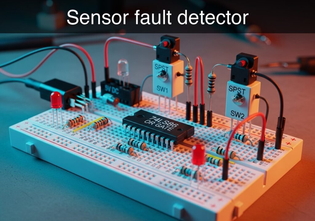
Level: Basic – Implement an XOR gate circuit to activate a visual alarm when two redundant sensors present different logic states.
Objective and use case
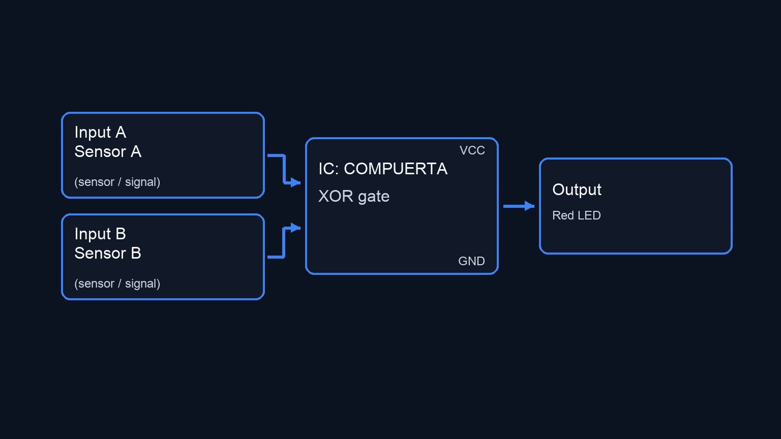
You will build a digital logic comparator circuit using a 74LS86 XOR (Exclusive-OR) gate to monitor two redundant switches acting as system sensors. The circuit evaluates the inputs continuously and activates a visual LED alarm only when the two sensors report conflicting states, indicating a potential sensor failure.
This circuit is highly useful in practical scenarios such as:
* Industrial automation, for monitoring dual-redundant safety limit switches on heavy machinery.
* Aerospace and aviation control systems, to detect disagreements between redundant flight sensors.
* Basic logic fault-detection training for maintenance and electronics technicians.
Expected outcome:
* A high output logic level (VOUT > 2.4 V) triggering the LED when the sensor states do not match.
* A low output logic level (VOUT < 0.4 V) keeping the LED turned off when both sensors agree (both HIGH or both LOW).
* A clear, immediate visual indication of logic discrepancies to the operator.
Target audience: Basic-level students learning digital logic gates, boolean algebra, and redundancy systems.
Materials
- V1: 5 V DC supply, function: primary power source
- SW1: SPST switch, function: redundant sensor A simulator
- SW2: SPST switch, function: redundant sensor B simulator
- R1: 10 kΩ resistor, function: pull-down for VA
- R2: 10 kΩ resistor, function: pull-down for VB
- R3: 330 Ω resistor, function: LED current limiting
- U1: 74LS86 Quad 2-Input Exclusive-OR Gate, function: fault detection logic
- D1: red LED, function: visual fault alarm indicator
Pin-out of the IC used
Integrated Circuit: 74LS86
| Pin | Name | Logic function | Connection in this case |
|---|---|---|---|
| 1 | 1 A | Input 1 for Gate 1 | Node VA (from SW1) |
| 2 | 1B | Input 2 for Gate 1 | Node VB (from SW2) |
| 3 | 1Y | Output of Gate 1 | Node VOUT (to R3 and D1) |
| 7 | GND | Ground | Node 0 (GND) |
| 14 | VCC | Power Supply | Node VCC (5 V) |
Note: Pins 4, 5, 6, 8, 9, 10, 11, 12, and 13 belong to the other three unused XOR gates. It is highly recommended to tie unused inputs (pins 4, 5, 9, 10, 12, 13) to Node 0 (GND).
Wiring guide
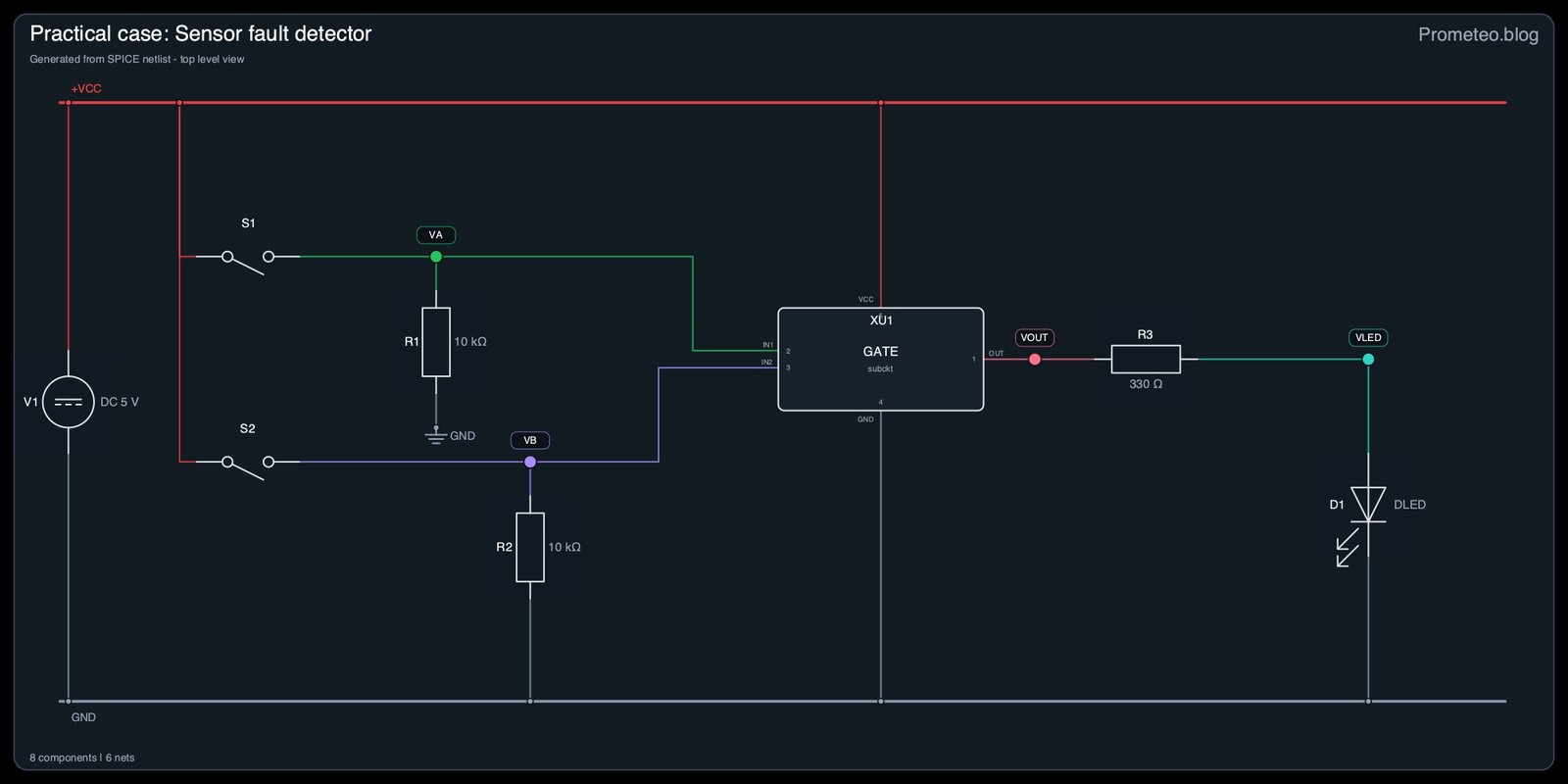
- V1: connects between VCC and 0.
- SW1: connects between VCC and VA.
- SW2: connects between VCC and VB.
- R1: connects between VA and 0.
- R2: connects between VB and 0.
- U1: connects Pin 14 to VCC, Pin 7 to 0, Pin 1 to VA, Pin 2 to VB, and Pin 3 to VOUT.
- R3: connects between VOUT and VLED.
- D1: connects its anode to VLED and its cathode to 0.
Conceptual block diagram
Schematic
VCC --> [ SW1: Sensor A ] --(VA)-->
              |                   |
              v                   v
        [ R1: 10 kΩ ]            [ U1: 74LS86 XOR Gate ] --(VOUT)--> [ R3: 330 Ω ] --(VLED)--> [ D1: Red LED ] --> GND
              |                   ^
              v                   |
             GND                  |
                                  |
VCC --> [ SW2: Sensor B ] --(VB)-->
              |
              v
        [ R2: 10 kΩ ]
              |
              v
             GND
Electrical diagram
Truth table
| Sensor A (Node VA) | Sensor B (Node VB) | Output (Node VOUT) | Alarm State (D1) | System Status |
|---|---|---|---|---|
| 0 | 0 | 0 | OFF | Normal (Agreement) |
| 0 | 1 | 1 | ON | Fault (Disagreement) |
| 1 | 0 | 1 | ON | Fault (Disagreement) |
| 1 | 1 | 0 | OFF | Normal (Agreement) |
Measurements and tests
- System Normal (Low): Leave both SW1 and SW2 open. Measure the voltage at nodes VA and VB with a multimeter; both should read 0 V. Measure VOUT; it should be < 0.4 V. The LED D1 must be OFF.
- Sensor A Fault: Close SW1 (applying 5 V to VA) while leaving SW2 open (0 V at VB). Measure VOUT; it should read > 2.4 V. The LED D1 must turn ON.
- Sensor B Fault: Open SW1 (0 V at VA) and close SW2 (applying 5 V to VB). Measure VOUT; it should read > 2.4 V. The LED D1 must turn ON.
- System Normal (High): Close both SW1 and SW2 so that both VA and VB read 5 V. Measure VOUT; it should drop back to < 0.4 V. The LED D1 must be OFF.
SPICE netlist and simulation
Reference SPICE Netlist (ngspice) — excerptFull SPICE netlist (ngspice)
* Practical case: Sensor fault detector
.width out=256

* Main Power Supply
V1 VCC 0 DC 5

* Redundant Sensor A Simulator (Switch 1)
VCTRLA ctrlA 0 PULSE(0 5 0 1u 1u 50u 100u)
S1 VCC VA ctrlA 0 SWMOD

* Redundant Sensor B Simulator (Switch 2)
VCTRLB ctrlB 0 PULSE(0 5 0 1u 1u 100u 200u)
S2 VCC VB ctrlB 0 SWMOD

* Pull-down Resistors for Inputs
R1 VA 0 10k
R2 VB 0 10k

* Fault Detection Logic (74LS86 XOR Gate)
XU1 VOUT VA VB 0 VCC GATE
* ... (truncated in public view) ...
Copy this content into a .cir file and run with ngspice.
* Practical case: Sensor fault detector
.width out=256

* Main Power Supply
V1 VCC 0 DC 5

* Redundant Sensor A Simulator (Switch 1)
VCTRLA ctrlA 0 PULSE(0 5 0 1u 1u 50u 100u)
S1 VCC VA ctrlA 0 SWMOD

* Redundant Sensor B Simulator (Switch 2)
VCTRLB ctrlB 0 PULSE(0 5 0 1u 1u 100u 200u)
S2 VCC VB ctrlB 0 SWMOD

* Pull-down Resistors for Inputs
R1 VA 0 10k
R2 VB 0 10k

* Fault Detection Logic (74LS86 XOR Gate)
XU1 VOUT VA VB 0 VCC GATE

* Visual Fault Alarm Indicator (LED and Current Limiting Resistor)
R3 VOUT VLED 330
D1 VLED 0 DLED

* Component Models
.model SWMOD SW(VT=2.5 VH=0.2 RON=0.1 ROFF=100MEG)
.model DLED D(IS=1e-15 N=1.5 RS=10)

* XOR Gate Behavioural Subcircuit
* Continuous implementation to ensure robust convergence
.subckt GATE out in1 in2 gnd vcc
B1 out gnd V = V(vcc) * ( 1/(1+exp(-50*(V(in1)-2.5))) + 1/(1+exp(-50*(V(in2)-2.5))) - 2 * (1/(1+exp(-50*(V(in1)-2.5)))) * (1/(1+exp(-50*(V(in2)-2.5)))) )
.ends

* Simulation Directives
.tran 1u 400u
.print tran V(VA) V(VB) V(VOUT) V(VLED)
.op
.end
Simulation Results (Transient Analysis)

Show raw data table (562 rows)
Index   time            v(va)           v(vb)           v(vout)         v(vled)
0	0.000000e+00	4.999500e-04	4.999500e-04	5.297196e-54	9.094010e-30
1	1.000000e-08	4.999500e-04	4.999500e-04	5.297196e-54	7.969517e-41
2	2.000000e-08	4.999500e-04	4.999500e-04	5.297196e-54	-7.96952e-41
3	4.000000e-08	4.999500e-04	4.999500e-04	5.297196e-54	-3.48674e-51
4	8.000000e-08	4.999500e-04	4.999500e-04	5.297196e-54	1.402111e-51
5	1.600000e-07	4.999500e-04	4.999500e-04	5.297196e-54	5.297196e-54
6	3.200000e-07	4.999500e-04	4.999500e-04	5.297196e-54	5.297196e-54
7	3.637500e-07	4.999500e-04	4.999500e-04	5.297196e-54	5.297196e-54
8	4.403125e-07	4.999500e-04	4.999500e-04	5.297196e-54	5.297196e-54
9	4.615039e-07	4.999500e-04	4.999500e-04	5.297196e-54	5.297196e-54
10	4.985889e-07	4.999500e-04	4.999500e-04	5.297196e-54	5.297196e-54
11	5.088535e-07	4.999500e-04	4.999500e-04	5.297196e-54	5.297196e-54
12	5.268165e-07	4.999500e-04	4.999500e-04	5.297196e-54	5.297196e-54
13	5.467041e-07	4.999950e+00	4.999950e+00	1.329451e-51	1.329451e-51
14	5.864794e-07	4.999950e+00	4.999950e+00	-2.81145e-68	3.383370e-62
15	6.660299e-07	4.999950e+00	4.999950e+00	-2.81145e-68	-2.26159e-62
16	8.251311e-07	4.999950e+00	4.999950e+00	-2.81145e-68	-2.81157e-68
17	1.000000e-06	4.999950e+00	4.999950e+00	-2.81145e-68	-2.81143e-68
18	1.031820e-06	4.999950e+00	4.999950e+00	-2.81145e-68	-2.81145e-68
19	1.095461e-06	4.999950e+00	4.999950e+00	-2.81145e-68	-2.81145e-68
20	1.222742e-06	4.999950e+00	4.999950e+00	-2.81145e-68	-2.81145e-68
21	1.477303e-06	4.999950e+00	4.999950e+00	-2.81145e-68	-2.81145e-68
22	1.986427e-06	4.999950e+00	4.999950e+00	-2.81145e-68	-2.81145e-68
23	2.986427e-06	4.999950e+00	4.999950e+00	-2.81145e-68	-2.81145e-68
... (538 more rows) ...
Reference SPICE netlist (ngspice)
* Practical case: Sensor fault detector
.width out=256

* Main Power Supply
V1 VCC 0 DC 5

* Redundant Sensor A Simulator (Switch 1)
VCTRLA ctrlA 0 PULSE(0 5 0 1u 1u 50u 100u)
S1 VCC VA ctrlA 0 SWMOD

* Redundant Sensor B Simulator (Switch 2)
VCTRLB ctrlB 0 PULSE(0 5 0 1u 1u 100u 200u)
S2 VCC VB ctrlB 0 SWMOD

* Pull-down Resistors for Inputs
R1 VA 0 10k
R2 VB 0 10k

* Fault Detection Logic (74LS86 XOR Gate)
XU1 VOUT VA VB 0 VCC GATE

* Visual Fault Alarm Indicator (LED and Current Limiting Resistor)
R3 VOUT VLED 330
D1 VLED 0 DLED

* Component Models
.model SWMOD SW(VT=2.5 VH=0.2 RON=0.1 ROFF=100MEG)
.model DLED D(IS=1e-15 N=1.5 RS=10)

* XOR Gate Behavioural Subcircuit
* Continuous implementation to ensure robust convergence
.subckt GATE out in1 in2 gnd vcc
B1 out gnd V = V(vcc) * ( 1/(1+exp(-50*(V(in1)-2.5))) + 1/(1+exp(-50*(V(in2)-2.5))) - 2 * (1/(1+exp(-50*(V(in1)-2.5)))) * (1/(1+exp(-50*(V(in2)-2.5)))) )
.ends

* Simulation Directives
.tran 1u 400u
.print tran V(VA) V(VB) V(VOUT) V(VLED)
.op
.end
Simulation Results (Transient Analysis)
Common mistakes and how to avoid them
- Forgetting pull-down resistors: Connecting the switches directly to the IC without R1 and R2 leaves the inputs floating when the switches are open, causing unpredictable behavior and false alarms. Always use pull-down resistors.
- LED polarity reversal: Putting the LED in backward (cathode to VLED, anode to 0) will prevent it from lighting up even when a fault is detected. Verify the flat edge or shorter leg is connected to ground.
- Leaving unused inputs floating: The 74LS86 contains four XOR gates. Leaving the inputs of the unused gates disconnected can cause internal oscillation and increase power consumption. Tie unused inputs to ground (0).
Troubleshooting
- Symptom: The LED never turns on under any switch combination.
- Cause: Faulty LED, backward LED polarity, broken R3 connection, or missing VCC/GND to the chip.
- Fix: Check D1 orientation. Verify 5 V at Pin 14 and 0 V at Pin 7 of U1.
- Symptom: The LED is always on, even when both switches are open or both are closed.
- Cause: One of the inputs is floating (missing pull-down resistor R1 or R2), or a switch is wired incorrectly.
- Fix: Check continuity on R1 and R2 to ground. Verify the voltages at VA and VB correspond strictly to the truth table.
- Symptom: The LED lights up correctly but is very dim.
- Cause: The 74LS series has weak current sourcing capabilities compared to modern CMOS chips, or the value of R3 is too high.
- Fix: Reduce R3 slightly (e.g., to 220 Ω), or see the extensions below for a better way to drive the LED.
Possible improvements and extensions
- Active-low output configuration: Since TTL chips (like the 74LS series) are much better at sinking current than sourcing it, rewire the LED so the anode goes to 5 V (through R3) and the cathode goes to VOUT. Note: you will need to add a NOT gate (e.g., 74LS04) after the XOR to invert the logic so the LED still turns on only during a fault.
- Audible alarm integration: Add an NPN transistor (like a 2N2222) connected to the XOR output via a base resistor. Use the transistor to drive a 5 V buzzer to provide both audible and visual alerts when the sensors disagree.
More Practical Cases on Prometeo.blog
Find this product and/or books on this topic on Amazon
As an Amazon Associate, I earn from qualifying purchases. If you buy through this link, you help keep this project running.
Quick Quiz

Telecommunications Electronics Engineer and Computer Engineer (official degrees in Spain).