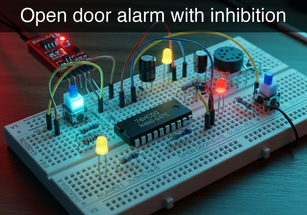
Practical case: Open door alarm with inhibition

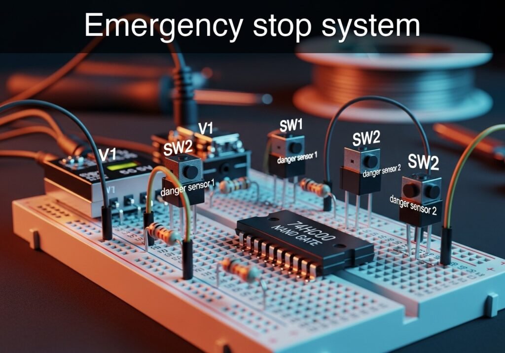
Open door alarm with inhibition prototype (Maker Style)

Level: Basic – Design a logic circuit using a 74HC00 NAND gate to trigger an LED alarm only when the door is open and the system is enabled.

Objective and use case

What you will build is a basic security system logic controller using the universal 74HC00 NAND chip. The circuit processes two discrete inputs (a door sensor and an enable switch) to activate a visual alarm strictly when the system is armed and a breach occurs.

Why it is useful:
* It demonstrates how multiple NAND gates can be combined to form an AND logic gate.
* It illustrates the concept of a hardware «enable/inhibit» signal commonly used in industrial and digital electronics.
* It provides practical experience in interfacing mechanical switches with digital CMOS inputs without floating states.

Expected outcome:
* When the door switch is open (Logic 1) AND the enable switch is closed (Logic 1), the LED turns ON.
* If the enable switch is open (Logic 0), the alarm remains inhibited (LED OFF) regardless of the door state.
* Logic High (VCC) and Logic Low (0 V) voltages can be clearly measured at the switch output nodes.
* The intermediate logic signal between the two NAND gates will correctly show the inverted state of the final output.

Target audience and level: Electronics beginners learning digital logic and combinational circuits.

Materials

  • V1: 5 V DC supply, function: main circuit power
  • SW1: SPST switch, function: door sensor (closed = logic 0, open = logic 1)
  • SW2: SPST switch, function: system enable (inhibited = logic 0, armed = logic 1)
  • R1: 10 kΩ resistor, function: pull-down for SW1 at node DOOR
  • R2: 10 kΩ resistor, function: pull-down for SW2 at node EN
  • R3: 330 Ω resistor, function: LED current limiting
  • U1: 74HC00 quad 2-input NAND gate, function: logic processing
  • D1: red LED, function: visual alarm indicator

Pin-out of the IC used

IC used: 74HC00 (Quad 2-Input NAND Gate)

Pin Name Logic function Connection in this case
1 1 A Input A of Gate 1 Node DOOR (from SW1)
2 1B Input B of Gate 1 Node EN (from SW2)
3 1Y Output of Gate 1 Node NAND_OUT
4 2 A Input A of Gate 2 Node NAND_OUT (tied to 2B)
5 2B Input B of Gate 2 Node NAND_OUT (tied to 2 A)
6 2Y Output of Gate 2 Node ALARM
7 GND Ground reference Node 0
14 VCC Positive supply Node VCC

(Note: Unused input pins 9, 10, 12, and 13 should be tied to ground in physical builds to prevent CMOS oscillation.)

Wiring guide

  • V1: connects between VCC (positive) and 0 (GND).
  • SW1: connects between VCC and DOOR.
  • R1: connects between DOOR and 0.
  • SW2: connects between VCC and EN.
  • R2: connects between EN and 0.
  • U1:
  • Pin 1 connects to DOOR.
  • Pin 2 connects to EN.
  • Pin 3 connects to NAND_OUT.
  • Pin 4 connects to NAND_OUT.
  • Pin 5 connects to NAND_OUT.
  • Pin 6 connects to ALARM.
  • Pin 7 connects to 0.
  • Pin 14 connects to VCC.
  • R3: connects between ALARM and LED_IN.
  • D1: anode connects to LED_IN, cathode connects to 0.

Conceptual block diagram
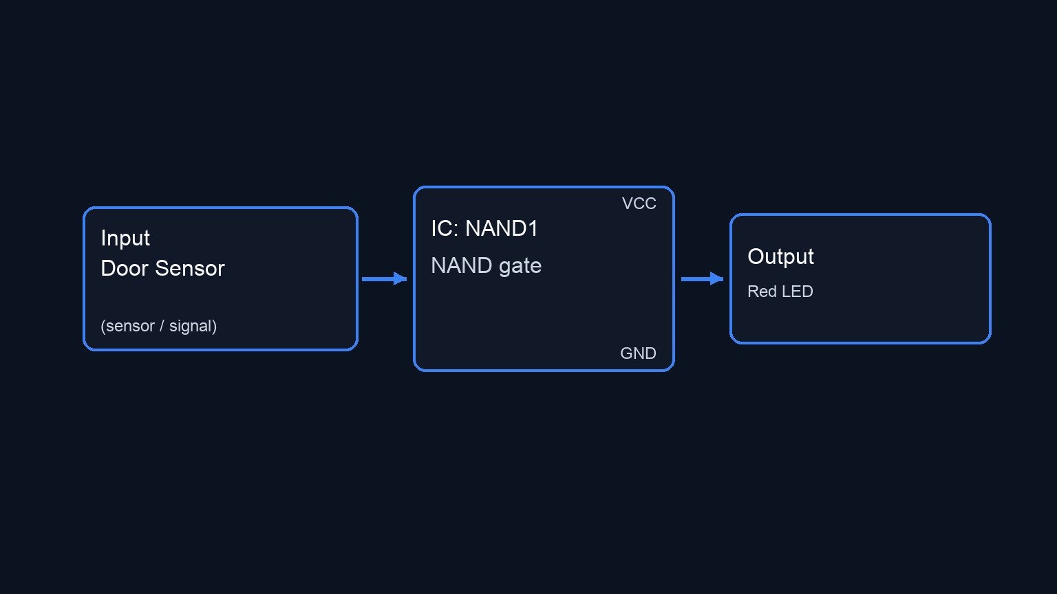
Conceptual block diagram — NAND1 NAND gate
Quick read: inputs → main block → output (actuator or measurement). This summarizes the ASCII schematic below.

Schematic

VCC --> [ SW1: Door Sensor ] --+--(DOOR)----->+
                               |              |
                         [ R1: 10 kΩ ]         v
                               |        [ U1: NAND1 ] --(NAND_OUT)--> [ U1: NAND2 ] --(ALARM)--> [ R3: 330 Ω ] --(LED_IN)--> [ D1: Red LED ] --> GND
                              GND       [ Pins 1,2->3 ]               [ Pins 4,5->6 ]
                                              ^
                                              |
VCC --> [ SW2: Sys Enable ] ---+--(EN)------->+
                               |
                         [ R2: 10 kΩ ]
                               |
                              GND
Electrical Schematic

Truth table

DOOR (SW1) EN (SW2) NAND_OUT (Pin 3) ALARM (Pin 6) LED Status
0 (Low) 0 (Low) 1 (High) 0 (Low) OFF
0 (Low) 1 (High) 1 (High) 0 (Low) OFF
1 (High) 0 (Low) 1 (High) 0 (Low) OFF
1 (High) 1 (High) 0 (Low) 1 (High) ON (Alarm Active)

Measurements and tests

  1. Supply Validation: Measure the voltage between VCC and 0. Ensure it is a stable 5 V.
  2. Input States: Use a multimeter to measure nodes DOOR and EN with respect to ground (0). Verify they read 0 V when the switch is open and 5 V when the switch is closed.
  3. Intermediate Logic: Close both SW1 and SW2. Measure node NAND_OUT. It should drop to 0 V (Logic Low) only when both switches are closed.
  4. Final Output: Measure node ALARM. It should read 5 V (Logic High) only when both switches are closed, confirming that U1B correctly inverted the signal from U1 A.
  5. Load Check: Verify the voltage drop across D1 is roughly 1.8 V to 2.2 V when illuminated.

SPICE netlist and simulation

Reference SPICE Netlist (ngspice) — excerptFull SPICE netlist (ngspice)

* Practical case: Open door alarm with inhibition
.width out=256

* Main Power Supply
V1 VCC 0 DC 5

* Door Sensor (SW1) - Modeled as a voltage-controlled switch with a pulse source
V_ctrl1 ctrl1 0 PULSE(0 5 0 1u 1u 50u 100u)
S1 VCC DOOR ctrl1 0 mySW
R1 DOOR 0 10k

* System Enable (SW2) - Modeled as a voltage-controlled switch with a slower pulse source
V_ctrl2 ctrl2 0 PULSE(0 5 0 1u 1u 100u 200u)
S2 VCC EN ctrl2 0 mySW
R2 EN 0 10k

* 74HC00 Quad 2-input NAND gate
* Wiring: 1->DOOR, 2->EN, 3->NAND_OUT, 4->NAND_OUT, 5->NAND_OUT, 6->ALARM, 7->0, 14->VCC
XU1 DOOR EN NAND_OUT NAND_OUT NAND_OUT ALARM 0 VCC 74HC00

* ... (truncated in public view) ...

Copy this content into a .cir file and run with ngspice.

* Practical case: Open door alarm with inhibition
.width out=256

* Main Power Supply
V1 VCC 0 DC 5

* Door Sensor (SW1) - Modeled as a voltage-controlled switch with a pulse source
V_ctrl1 ctrl1 0 PULSE(0 5 0 1u 1u 50u 100u)
S1 VCC DOOR ctrl1 0 mySW
R1 DOOR 0 10k

* System Enable (SW2) - Modeled as a voltage-controlled switch with a slower pulse source
V_ctrl2 ctrl2 0 PULSE(0 5 0 1u 1u 100u 200u)
S2 VCC EN ctrl2 0 mySW
R2 EN 0 10k

* 74HC00 Quad 2-input NAND gate
* Wiring: 1->DOOR, 2->EN, 3->NAND_OUT, 4->NAND_OUT, 5->NAND_OUT, 6->ALARM, 7->0, 14->VCC
XU1 DOOR EN NAND_OUT NAND_OUT NAND_OUT ALARM 0 VCC 74HC00

* Alarm LED indicator
R3 ALARM LED_IN 330
D1 LED_IN 0 DLED

* Models and Subcircuits
.model mySW SW(Ron=1 Roff=100Meg Vt=2.5)
.model DLED D(IS=1e-15 N=2 RS=10)

* 74HC00 Subcircuit implementation (using robust continuous B-sources for logic)
.subckt 74HC00 1 2 3 4 5 6 7 14
* Gate 1 (Pins 1, 2 -> 3)
B1 3 7 V = 5 * (1 - (1 / (1 + exp(-50*(V(1,7)-2.5)))) * (1 / (1 + exp(-50*(V(2,7)-2.5)))))
* Gate 2 (Pins 4, 5 -> 6)
B2 6 7 V = 5 * (1 - (1 / (1 + exp(-50*(V(4,7)-2.5)))) * (1 / (1 + exp(-50*(V(5,7)-2.5)))))
* Dummy loads to prevent floating pins
R1 1 7 100Meg
R2 2 7 100Meg
R3 4 7 100Meg
R4 5 7 100Meg
R5 14 7 100Meg
.ends

* Analysis Directives
.op
.tran 1u 300u
.print tran V(DOOR) V(EN) V(ALARM) V(LED_IN)
.end

Simulation Results (Transient Analysis)

Simulation Results (Transient Analysis)
Analysis: The simulation results show that when both DOOR and EN are high (approx 5V), ALARM goes high (5V) and LED_IN reaches about 1.65V, indicating the LED is ON. When either DOOR or EN is low (approx 0V), ALARM is low (0V) and LED_IN is 0V, indicating the LED is OFF. This perfectly matches the intended truth table for the alarm with inhibition.
Show raw data table (412 rows)
Index   time            v(door)         v(en)           v(alarm)        v(led_in)
0	0.000000e+00	4.999000e-04	4.999000e-04	-7.41841e-68	4.091162e-30
1	1.000000e-08	4.999000e-04	4.999000e-04	-7.41841e-68	2.688961e-41
2	2.000000e-08	4.999000e-04	4.999000e-04	-7.41841e-68	-2.68896e-41
3	4.000000e-08	4.999000e-04	4.999000e-04	-7.41841e-68	-8.83675e-52
4	8.000000e-08	4.999000e-04	4.999000e-04	-7.41841e-68	3.534698e-52
5	1.600000e-07	4.999000e-04	4.999000e-04	-7.41841e-68	1.858568e-62
6	3.200000e-07	4.999000e-04	4.999000e-04	-7.41841e-68	-4.64651e-63
7	3.562500e-07	4.999000e-04	4.999000e-04	-7.41841e-68	-7.41842e-68
8	4.196875e-07	4.999000e-04	4.999000e-04	-7.41841e-68	-7.41841e-68
9	4.372461e-07	4.999000e-04	4.999000e-04	-7.41841e-68	-7.41841e-68
10	4.679736e-07	4.999000e-04	4.999000e-04	-7.41841e-68	-7.41841e-68
11	5.019934e-07	4.999500e+00	4.999500e+00	5.000000e+00	1.651140e+00
12	5.700330e-07	4.999500e+00	4.999500e+00	5.000000e+00	1.651062e+00
13	7.061121e-07	4.999500e+00	4.999500e+00	5.000000e+00	1.650721e+00
14	9.782703e-07	4.999500e+00	4.999500e+00	5.000000e+00	1.650725e+00
15	1.000000e-06	4.999500e+00	4.999500e+00	5.000000e+00	1.650721e+00
16	1.043459e-06	4.999500e+00	4.999500e+00	5.000000e+00	1.650721e+00
17	1.130378e-06	4.999500e+00	4.999500e+00	5.000000e+00	1.650721e+00
18	1.304216e-06	4.999500e+00	4.999500e+00	5.000000e+00	1.650721e+00
19	1.651892e-06	4.999500e+00	4.999500e+00	5.000000e+00	1.650721e+00
20	2.347244e-06	4.999500e+00	4.999500e+00	5.000000e+00	1.650721e+00
21	3.347244e-06	4.999500e+00	4.999500e+00	5.000000e+00	1.650721e+00
22	4.347244e-06	4.999500e+00	4.999500e+00	5.000000e+00	1.650721e+00
23	5.347244e-06	4.999500e+00	4.999500e+00	5.000000e+00	1.650721e+00
... (388 more rows) ...


Reference SPICE netlist (ngspice)

* Practical case: Open door alarm with inhibition
.width out=256

* Main Power Supply
V1 VCC 0 DC 5

* Door Sensor (SW1) - Modeled as a voltage-controlled switch with a pulse source
V_ctrl1 ctrl1 0 PULSE(0 5 0 1u 1u 50u 100u)
S1 VCC DOOR ctrl1 0 mySW
R1 DOOR 0 10k

* System Enable (SW2) - Modeled as a voltage-controlled switch with a slower pulse source
V_ctrl2 ctrl2 0 PULSE(0 5 0 1u 1u 100u 200u)
S2 VCC EN ctrl2 0 mySW
R2 EN 0 10k

* 74HC00 Quad 2-input NAND gate
* Wiring: 1->DOOR, 2->EN, 3->NAND_OUT, 4->NAND_OUT, 5->NAND_OUT, 6->ALARM, 7->0, 14->VCC
XU1 DOOR EN NAND_OUT NAND_OUT NAND_OUT ALARM 0 VCC 74HC00

* Alarm LED indicator
R3 ALARM LED_IN 330
D1 LED_IN 0 DLED

* Models and Subcircuits
.model mySW SW(Ron=1 Roff=100Meg Vt=2.5)
.model DLED D(IS=1e-15 N=2 RS=10)

* 74HC00 Subcircuit implementation (using robust continuous B-sources for logic)
.subckt 74HC00 1 2 3 4 5 6 7 14
* Gate 1 (Pins 1, 2 -> 3)
B1 3 7 V = 5 * (1 - (1 / (1 + exp(-50*(V(1,7)-2.5)))) * (1 / (1 + exp(-50*(V(2,7)-2.5)))))
* Gate 2 (Pins 4, 5 -> 6)
B2 6 7 V = 5 * (1 - (1 / (1 + exp(-50*(V(4,7)-2.5)))) * (1 / (1 + exp(-50*(V(5,7)-2.5)))))
* Dummy loads to prevent floating pins
R1 1 7 100Meg
R2 2 7 100Meg
R3 4 7 100Meg
R4 5 7 100Meg
R5 14 7 100Meg
.ends

* Analysis Directives
.op
.tran 1u 300u
.print tran V(DOOR) V(EN) V(ALARM) V(LED_IN)
.end

Simulation Results (Transient Analysis)

Simulation Results (Transient Analysis)
Analysis: The simulation results show that when both DOOR and EN are high (approx 5V), ALARM goes high (5V) and LED_IN reaches about 1.65V, indicating the LED is ON. When either DOOR or EN is low (approx 0V), ALARM is low (0V) and LED_IN is 0V, indicating the LED is OFF. This perfectly matches the intended truth table for the alarm with inhibition.

Common mistakes and how to avoid them

  • Floating CMOS inputs: Forgetting the pull-down resistors (R1, R2) will leave the inputs floating when the switches are open, causing unpredictable LED blinking and excessive IC current draw. Always ensure mechanical switches are paired with pull-up or pull-down resistors.
  • Leaving unused gates floating: The 74HC00 contains four gates. Leaving the inputs of gates 3 and 4 disconnected can cause high-frequency oscillations. Tie pins 8, 9, 12, and 13 to ground (0).
  • Misunderstanding NAND logic for NOT: To use a NAND gate as an inverter (NOT gate), you must tie both inputs together (as done on pins 4 and 5). Supplying the signal to only one pin while leaving the other floating will result in faulty logic.


Troubleshooting

  • Symptom: The LED never turns on.
  • Cause: D1 might be inserted backward (reverse polarity), or R3 is too large.
  • Fix: Check that the long leg (anode) of D1 faces ALARM and the flat side (cathode) goes to 0. Verify R3 is 330 Ω, not 330 kΩ.
  • Symptom: The LED turns on as soon as one switch is closed, ignoring the other.
  • Cause: A wiring error on the 74HC00 inputs, or an input pin is shorted to VCC.
  • Fix: Check continuity on pins 1 and 2. Ensure they are isolated from each other and correctly routed to DOOR and EN.
  • Symptom: The circuit is highly sensitive to hand movements nearby.
  • Cause: Floating inputs. The pull-down resistors are either disconnected or not making good contact on the breadboard.
  • Fix: Verify R1 and R2 are securely connected between the switch signal nodes and ground.

Possible improvements and extensions

  • Active Buzzer Integration: Add a 5 V active buzzer in parallel with the LED (and its resistor) so the alarm provides both visual and auditory feedback.
  • Flashing Alarm: Use the two remaining NAND gates in the 74HC00 along with a resistor and capacitor to build an astable multivibrator, making the LED blink repeatedly when the alarm is triggered instead of staying solid.

More Practical Cases on Prometeo.blog

Find this product and/or books on this topic on Amazon

Go to Amazon

As an Amazon Associate, I earn from qualifying purchases. If you buy through this link, you help keep this project running.

Quick Quiz

Question 1: What is the main objective of the circuit described in the text?


Question 2: Which specific logic chip is used as the core of this circuit?


Question 3: Under what exact condition does the LED alarm turn ON?


Question 4: What logic function is created by combining multiple NAND gates in this project?


Question 5: How does the circuit handle mechanical switches connected to digital CMOS inputs?


Question 6: What happens if the enable switch is open (Logic 0)?


Question 7: What concept commonly used in industrial electronics does this project illustrate?


Question 8: What logic level represents an open door in this circuit?


Question 9: What will the intermediate logic signal between the two NAND gates show?


Question 10: What voltages can be clearly measured at the switch output nodes?


Carlos Núñez Zorrilla
Electronics & Computer Engineer

Telecommunications Electronics Engineer and Computer Engineer (official degrees in Spain).
Follow me:


Practical case: Emergency stop system

Emergency stop system prototype (Maker Style)

Level: Basic – Use the low-level output of a NAND gate to stop a process if two sensors detect danger simultaneously.

Objective and use case

In this practical case, you will build a digital safety interlock circuit using a 74HC00 NAND gate. The system evaluates two independent danger sensors and triggers an active-low relay to halt a process only when both sensors detect a critical condition.

Why it is useful:
* Industrial safety: Halting heavy machinery if two separate safety guards are simultaneously bypassed or opened.
* Process control: Triggering an emergency shutdown in a chemical plant if both pressure and temperature exceed critical thresholds.
* Redundant validation: Preventing false alarms from shutting down a system by requiring two independent sensors to agree before taking action.

Expected outcome:
* When both sensors read a HIGH logic level (indicating danger), the NAND gate output will drop to a LOW logic level (~0 V).
* The 0 V signal will trigger an active-low relay module, engaging the emergency stop.
* If either or both sensors read a LOW logic level (safe condition), the NAND output remains HIGH (~5 V), keeping the relay inactive and the process running.

Target audience and level: Beginners in digital electronics and industrial logic control.

Materials

  • V1: 5 V DC power supply
  • SW1: SPST switch, function: danger sensor 1
  • SW2: SPST switch, function: danger sensor 2
  • R1: 10 kΩ resistor, function: pull-down for SW1
  • R2: 10 kΩ resistor, function: pull-down for SW2
  • U1: 74HC00 Quad 2-Input NAND gate IC
  • RLY1: 5 V Active-low relay module, function: process emergency stop

Pin-out of the IC used

We will use the 74HC00 (Quad 2-Input NAND gate).

Pin Name Logic function Connection in this case
1 1 A Input 1 of Gate 1 Node VA (from SW1)
2 1B Input 2 of Gate 1 Node VB (from SW2)
3 1Y Output of Gate 1 Node VOUT (to RLY1 IN)
7 GND Ground Node 0
14 VCC Power Supply Node VCC

Wiring guide

  • V1: connects between node VCC and node 0 (GND).
  • SW1: connects between node VCC and node VA.
  • R1: connects between node VA and node 0.
  • SW2: connects between node VCC and node VB.
  • R2: connects between node VB and node 0.
  • U1: Pin 14 connects to node VCC; Pin 7 connects to node 0.
  • U1: Pin 1 connects to node VA.
  • U1: Pin 2 connects to node VB.
  • U1: Pin 3 connects to node VOUT.
  • RLY1: VCC pin connects to node VCC, GND pin connects to node 0, and the signal/IN pin connects to node VOUT.

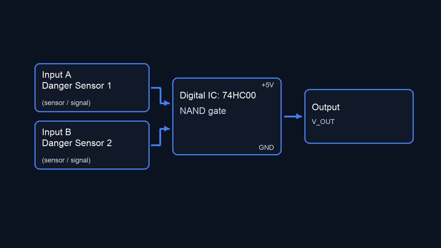
Conceptual block diagram

Conceptual block diagram — 74HC00 NAND gate
Quick read: inputs → main block → output (actuator or measurement). This summarizes the ASCII schematic below.

Schematic

POWER SUPPLY:
[ V1: 5 V DC Power Supply ] --(VCC)
                           --(GND)

SENSOR 1 INPUT PATH:
VCC --> [ SW1: Danger Sensor 1 ] --(Node VA)--> [ U1: 74HC00 NAND (Pin 1) ]
[ Node VA ] --> [ R1: 10 kΩ Pull-down ] --> GND

SENSOR 2 INPUT PATH:
VCC --> [ SW2: Danger Sensor 2 ] --(Node VB)--> [ U1: 74HC00 NAND (Pin 2) ]
[ Node VB ] --> [ R2: 10 kΩ Pull-down ] --> GND

LOGIC TO EMERGENCY STOP PATH:
[ U1: 74HC00 NAND (Pin 3) ] --(Node VOUT)--> [ RLY1: Relay Module (IN) ]

IC & MODULE POWER CONNECTIONS:
VCC --> [ U1: 74HC00 NAND (Pin 14) ]
GND <-- [ U1: 74HC00 NAND (Pin 7) ]

VCC --> [ RLY1: Relay Module (VCC) ]
GND <-- [ RLY1: Relay Module (GND) ]
Electrical Schematic

Truth table

Note: The relay module in this case is active-low, meaning it triggers the emergency stop when it receives a 0.

SW1 (Node VA) SW2 (Node VB) VOUT (NAND Output) Relay State (Active-Low) Process Status
0 (Safe) 0 (Safe) 1 (HIGH) OFF Running
0 (Safe) 1 (Danger) 1 (HIGH) OFF Running
1 (Danger) 0 (Safe) 1 (HIGH) OFF Running
1 (Danger) 1 (Danger) 0 (LOW) ON (Triggered) STOPPED

Measurements and tests

  1. Input Logic States: Using a digital multimeter, measure the DC voltage at nodes VA and VB with respect to node 0. Verify they read ~0 V when the switches are open, and ~5 V when closed.
  2. Output Voltage Level: Measure node VOUT. Confirm it sits near 5 V during normal operation (when one or zero switches are closed).
  3. System Activation: Close both SW1 and SW2 simultaneously. Measure node VOUT to ensure it drops to ~0 V.
  4. Relay Actuation: Listen for the audible «click» of the relay (or observe its onboard indicator LED) precisely when VOUT drops to 0 V, confirming the emergency stop command has been physically executed.

SPICE netlist and simulation

Reference SPICE Netlist (ngspice) — excerptFull SPICE netlist (ngspice)

* Practical case: Emergency stop system
.width out=256

* Main 5V DC power supply
V1 VCC 0 DC 5

* SW1 (Danger sensor 1) and its pull-down resistor
S1 VCC VA ctrl1 0 sw_mod
Vctrl1 ctrl1 0 PULSE(0 5 0 1u 1u 50u 100u)
R1 VA 0 10k

* SW2 (Danger sensor 2) and its pull-down resistor
S2 VCC VB ctrl2 0 sw_mod
Vctrl2 ctrl2 0 PULSE(0 5 0 1u 1u 100u 200u)
R2 VB 0 10k

* U1: 74HC00 Quad 2-Input NAND gate IC (Using pins 1, 2, 3, 7, 14)
XU1 VA VB VOUT VCC 0 NAND_74HC00

* RLY1: 5V Active-low relay module
* ... (truncated in public view) ...

Copy this content into a .cir file and run with ngspice.

* Practical case: Emergency stop system
.width out=256

* Main 5V DC power supply
V1 VCC 0 DC 5

* SW1 (Danger sensor 1) and its pull-down resistor
S1 VCC VA ctrl1 0 sw_mod
Vctrl1 ctrl1 0 PULSE(0 5 0 1u 1u 50u 100u)
R1 VA 0 10k

* SW2 (Danger sensor 2) and its pull-down resistor
S2 VCC VB ctrl2 0 sw_mod
Vctrl2 ctrl2 0 PULSE(0 5 0 1u 1u 100u 200u)
R2 VB 0 10k

* U1: 74HC00 Quad 2-Input NAND gate IC (Using pins 1, 2, 3, 7, 14)
XU1 VA VB VOUT VCC 0 NAND_74HC00

* RLY1: 5V Active-low relay module
XRLY1 VOUT VCC 0 RELAY_MOD

* --- Subcircuits ---

.subckt NAND_74HC00 INA INB OUT VCC GND
* Behavioral NAND gate using continuous sigmoid functions for robust convergence
B1 OUT_int 0 V = 5 * (1 - (1/(1+exp(-20*(V(INA)-2.5)))) * (1/(1+exp(-20*(V(INB)-2.5)))))
R1 OUT_int OUT 100
C1 OUT 0 10p
.ends

.subckt RELAY_MOD IN VCC GND
* Simple resistive model for the relay module to satisfy load requirements
R_in IN GND 10k
R_vcc VCC GND 1k
.ends

* --- Models ---
.model sw_mod SW(Vt=2.5 Ron=0.1 Roff=100Meg)

* --- Analysis Directives ---
.tran 1u 300u
.print tran V(VA) V(VB)
.op
.end

Simulation Results (Transient Analysis)

Simulation Results (Transient Analysis)
Analysis: The ngspice transient analysis shows nodes VA and VB toggling between approximately 0V and 5V, consistent with the PULSE sources driving the switches. This correctly simulates the different combinations of the danger sensors (SW1 and SW2) being triggered or safe.
Show raw data table (501 rows)
Index   time            v(va)           v(vb)
0	0.000000e+00	4.999500e-04	4.999500e-04
1	1.000000e-08	4.999500e-04	4.999500e-04
2	2.000000e-08	4.999500e-04	4.999500e-04
3	4.000000e-08	4.999500e-04	4.999500e-04
4	8.000000e-08	4.999500e-04	4.999500e-04
5	1.600000e-07	4.999500e-04	4.999500e-04
6	3.200000e-07	4.999500e-04	4.999500e-04
7	3.562500e-07	4.999500e-04	4.999500e-04
8	4.196875e-07	4.999500e-04	4.999500e-04
9	4.372461e-07	4.999500e-04	4.999500e-04
10	4.679736e-07	4.999500e-04	4.999500e-04
11	4.795524e-07	4.999500e-04	4.999500e-04
12	4.902290e-07	4.999500e-04	4.999500e-04
13	5.023412e-07	4.999950e+00	4.999950e+00
14	5.111724e-07	4.999950e+00	4.999950e+00
15	5.196372e-07	4.999950e+00	4.999950e+00
16	5.247062e-07	4.999950e+00	4.999950e+00
17	5.271308e-07	4.999950e+00	4.999950e+00
18	5.277087e-07	4.999950e+00	4.999950e+00
19	5.280739e-07	4.999950e+00	4.999950e+00
20	5.285244e-07	4.999950e+00	4.999950e+00
21	5.292184e-07	4.999950e+00	4.999950e+00
22	5.299733e-07	4.999950e+00	4.999950e+00
23	5.306602e-07	4.999950e+00	4.999950e+00
... (477 more rows) ...


Reference SPICE netlist (ngspice)

* Practical case: Emergency stop system
.width out=256

* Main 5V DC power supply
V1 VCC 0 DC 5

* SW1 (Danger sensor 1) and its pull-down resistor
S1 VCC VA ctrl1 0 sw_mod
Vctrl1 ctrl1 0 PULSE(0 5 0 1u 1u 50u 100u)
R1 VA 0 10k

* SW2 (Danger sensor 2) and its pull-down resistor
S2 VCC VB ctrl2 0 sw_mod
Vctrl2 ctrl2 0 PULSE(0 5 0 1u 1u 100u 200u)
R2 VB 0 10k

* U1: 74HC00 Quad 2-Input NAND gate IC (Using pins 1, 2, 3, 7, 14)
XU1 VA VB VOUT VCC 0 NAND_74HC00

* RLY1: 5V Active-low relay module
XRLY1 VOUT VCC 0 RELAY_MOD

* --- Subcircuits ---

.subckt NAND_74HC00 INA INB OUT VCC GND
* Behavioral NAND gate using continuous sigmoid functions for robust convergence
B1 OUT_int 0 V = 5 * (1 - (1/(1+exp(-20*(V(INA)-2.5)))) * (1/(1+exp(-20*(V(INB)-2.5)))))
R1 OUT_int OUT 100
C1 OUT 0 10p
.ends

.subckt RELAY_MOD IN VCC GND
* Simple resistive model for the relay module to satisfy load requirements
R_in IN GND 10k
R_vcc VCC GND 1k
.ends

* --- Models ---
.model sw_mod SW(Vt=2.5 Ron=0.1 Roff=100Meg)

* --- Analysis Directives ---
.tran 1u 300u
.print tran V(VA) V(VB)
.op
.end

Simulation Results (Transient Analysis)

Simulation Results (Transient Analysis)
Analysis: The ngspice transient analysis shows nodes VA and VB toggling between approximately 0V and 5V, consistent with the PULSE sources driving the switches. This correctly simulates the different combinations of the danger sensors (SW1 and SW2) being triggered or safe.

Common mistakes and how to avoid them

  • Floating inputs: Forgetting the pull-down resistors (R1 and R2). Without them, the logic gate inputs will float and pick up ambient noise, causing the relay to trigger randomly.
  • Misunderstanding active-low logic: Expecting the relay to trigger when the output is 5 V. In this case, the NAND output drops to 0 V upon detecting mutual danger, which perfectly matches an active-low relay module. Ensure your relay module is truly active-low.
  • Omitting IC power connections: Forgetting to wire pins 14 (VCC) and 7 (GND) of the 74HC00. The IC will not process logic without power, and may behave erratically if powered parasitically through its input pins.


Troubleshooting

  • Symptom: The relay never clicks, even when both switches are closed.
    • Cause: The 74HC00 output pin cannot sink enough current, or the relay module is active-high instead of active-low.
    • Fix: Ensure you are using a relay module (with a built-in driver transistor) rather than a bare mechanical relay. Verify the module’s trigger logic (some have a jumper to select active-high vs. active-low).
  • Symptom: The relay chatters rapidly or triggers randomly without human interaction.
    • Cause: Floating inputs at node VA or VB.
    • Fix: Double-check that R1 and R2 are properly seated in the breadboard and connected directly to GND (node 0).
  • Symptom: The relay is always ON, and the process is permanently stopped.
    • Cause: The NAND output is permanently stuck at 0 V. This can happen if both inputs are shorted to VCC, or if the logic gate is damaged.
    • Fix: Measure VA and VB. If they are reading 0 V but VOUT is still 0 V, replace the 74HC00 IC.

Possible improvements and extensions

  • Hardware debouncing: Add a 1 µF capacitor across each switch to prevent contact bounce from generating rapid, unintended logic transitions during the millisecond the switch is toggled.
  • Visual status indicators: Connect an LED and a 330 Ω current-limiting resistor to node VOUT to provide a clear visual indicator on a control panel when the system is in a safe state (LED ON) versus an emergency state (LED OFF).

More Practical Cases on Prometeo.blog

Find this product and/or books on this topic on Amazon

Go to Amazon

As an Amazon Associate, I earn from qualifying purchases. If you buy through this link, you help keep this project running.

Quick Quiz

Question 1: What is the main objective of the circuit described in the article?


Question 2: Which specific IC is used in this project?


Question 3: When will the active-low relay be triggered to halt the process?


Question 4: What logic level from the sensors indicates a 'danger' condition?


Question 5: What is the output of the NAND gate when both sensors read a HIGH logic level?


Question 6: What happens to the process if either or both sensors read a LOW logic level (safe condition)?


Question 7: Why is redundant validation useful in this circuit?


Question 8: What is an example of industrial safety mentioned in the text?


Question 9: What type of relay module is used for the process emergency stop?


Question 10: What is the difficulty level of this practical case?


Carlos Núñez Zorrilla
Electronics & Computer Engineer

Telecommunications Electronics Engineer and Computer Engineer (official degrees in Spain).
Follow me:


Practical case: Logic inverter using NAND gate

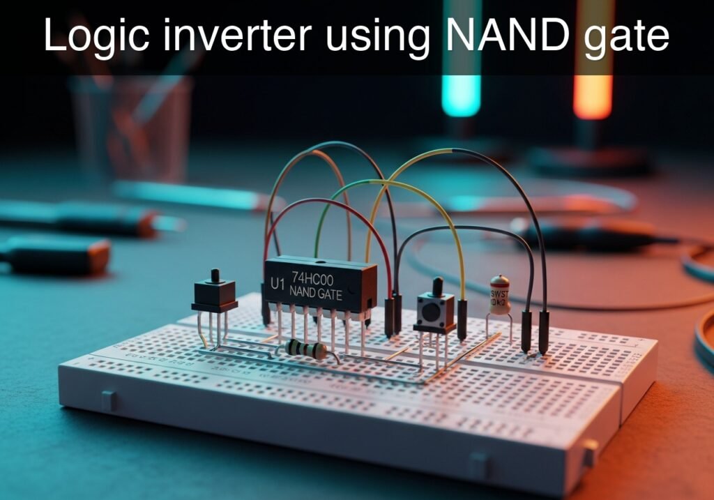
Logic inverter using NAND gate prototype (Maker Style)

Level: Basic – Demonstrate the universality of the NAND gate by configuring it as a basic NOT gate.

Objective and use case

In this practical case, you will build a digital inverter (NOT gate) using a standard 74HC00 NAND gate by shorting its inputs together.

Understanding this configuration is highly useful for several reasons:
* BOM Optimization: It reduces the number of unique integrated circuits needed in a design; if you have spare NAND gates on a board, you do not need to add a dedicated NOT gate chip.
* Logic Universality: It practically proves that NAND gates are «universal,» meaning any logic function can be constructed using only NAND gates.
* Circuit Simplification: It helps streamline routing on printed circuit boards by repurposing nearby unused gates instead of running traces to a different IC.

Expected outcome:
* When the input switch provides a logic LOW (0 V) to the shorted inputs, the output will go HIGH (approx. 5 V), turning on the indicator LED.
* When the input switch provides a logic HIGH (5 V) to the shorted inputs, the output will go LOW (0 V), turning off the indicator LED.
* The circuit will perfectly replicate the behavior of a standard 74HC04 NOT gate.

Target audience: Electronics beginners learning fundamental Boolean algebra and digital hardware implementation.

Materials

  • V1: 5 V DC supply
  • U1: 74HC00 Quad 2-Input NAND Gate
  • SW1: SPST toggle switch or push button, function: input state selector
  • R1: 10 kΩ resistor, function: pull-down for node VA
  • R2: 330 Ω resistor, function: current limiting for the output LED
  • D1: Red LED, function: VOUT state indicator

Pin-out of the IC used

IC: 74HC00 (Quad 2-Input NAND gate)

Pin Name Logic function Connection in this case
1 1 A Input A of Gate 1 Node VA (shorted to 1B)
2 1B Input B of Gate 1 Node VA (shorted to 1 A)
3 1Y Output of Gate 1 Node VOUT
7 GND Ground Node 0
14 VCC Positive Power Supply Node VCC

(Note: Pins 4, 5, 9, 10, 12, 13 are unused inputs in this specific exercise and should ideally be tied to Ground in a final physical circuit to prevent CMOS floating input issues).

Wiring guide

  • V1: Connects between node VCC (+5 V) and node 0 (GND).
  • U1 VCC/GND: Connect pin 14 to node VCC and pin 7 to node 0.
  • SW1: Connects between node VCC and node VA.
  • R1: Connects between node VA and node 0 (ensures a definitive LOW when the switch is open).
  • U1 Inputs: Connect pin 1 (1 A) to node VA and connect pin 2 (1B) to node VA. This ties both inputs of the first NAND gate together.
  • U1 Output: Pin 3 (1Y) provides the inverted signal and connects to node VOUT.
  • R2: Connects between node VOUT and the anode of D1.
  • D1: Connects the cathode to node 0.

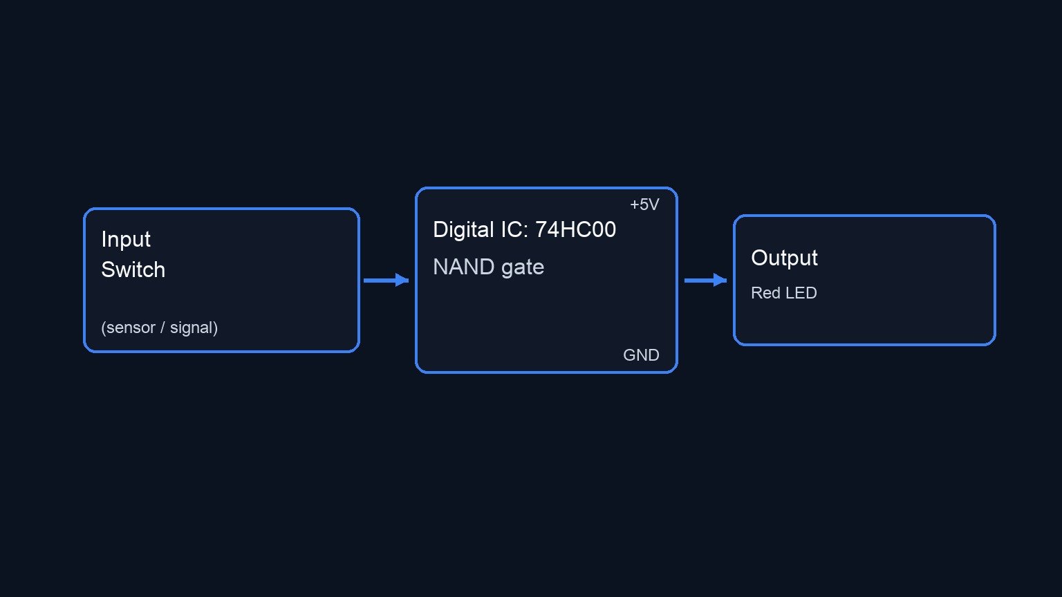
Conceptual block diagram

Conceptual block diagram — 74HC00 NAND gate
Quick read: inputs → main block → output (actuator or measurement). This summarizes the ASCII schematic below.

Schematic

VCC --> [ SW1: Switch ] --(Node VA)--> [ U1: 74HC00 NAND (Pins 1 & 2) ] --(VOUT)--> [ R2: 330 Ω ] --> [ D1: Red LED ] --> GND
                               |
                          [ R1: 10 kΩ ]
                               |
                              GND
Electrical Schematic

Truth table

Input (VA) Output (VOUT) LED State (D1)
0 (LOW) 1 (HIGH) ON
1 (HIGH) 0 (LOW) OFF

Measurements and tests

  1. Input Voltage Measurement: Use a multimeter to measure the voltage at node VA with respect to node 0. Verify that it reads ~0 V when SW1 is open, and ~5 V when SW1 is closed.
  2. Output Voltage Measurement: Move the multimeter probe to node VOUT. Confirm that it reads ~5 V when VA is 0 V, and reads ~0 V when VA is 5 V.
  3. Functional Verification: Toggle the switch multiple times. Ensure D1 behaves inversely to the physical action of the switch (e.g., if pressing the button sends a HIGH signal, the LED should turn off when pressed).

SPICE netlist and simulation

Reference SPICE Netlist (ngspice) — excerptFull SPICE netlist (ngspice)

* Practical case: Logic inverter using NAND gate

* Power Supply
V1 VCC 0 DC 5V

* Switch SW1 (VCC to VA)
* Modeled as a voltage-controlled switch to simulate user interaction
S_SW1 VCC VA SW_CTRL 0 sw_mod
.model sw_mod SW(vt=2.5 vh=0.2 ron=0.1 roff=100Meg)
V_SW_CTRL SW_CTRL 0 PULSE(0 5 10u 1u 1u 100u 200u)

* Pull-down resistor R1
R1 VA 0 10k

* U1: 74HC00 Quad 2-Input NAND Gate (using 1 gate)
* Pin 14: VCC, Pin 7: 0
* Pin 1: VA, Pin 2: VA, Pin 3: VOUT
XU1 VA VA VOUT VCC 0 NAND2_74HC00

* R2: Current limiting resistor
* ... (truncated in public view) ...

Copy this content into a .cir file and run with ngspice.

* Practical case: Logic inverter using NAND gate

* Power Supply
V1 VCC 0 DC 5V

* Switch SW1 (VCC to VA)
* Modeled as a voltage-controlled switch to simulate user interaction
S_SW1 VCC VA SW_CTRL 0 sw_mod
.model sw_mod SW(vt=2.5 vh=0.2 ron=0.1 roff=100Meg)
V_SW_CTRL SW_CTRL 0 PULSE(0 5 10u 1u 1u 100u 200u)

* Pull-down resistor R1
R1 VA 0 10k

* U1: 74HC00 Quad 2-Input NAND Gate (using 1 gate)
* Pin 14: VCC, Pin 7: 0
* Pin 1: VA, Pin 2: VA, Pin 3: VOUT
XU1 VA VA VOUT VCC 0 NAND2_74HC00

* R2: Current limiting resistor
R2 VOUT N1 330

* D1: Red LED
D1 N1 0 DLED

* Models
.model DLED D(IS=1e-15 N=1.8 RS=10)

* Subcircuit for NAND Gate
.subckt NAND2_74HC00 1A 1B 1Y VCC GND
RinA 1A GND 1G
RinB 1B GND 1G
Rvcc VCC GND 100Meg
B1 Y_int GND V = 5 * (1 - (1/(1+exp(-50*(V(1A)-2.5)))) * (1/(1+exp(-50*(V(1B)-2.5)))))
Rout Y_int 1Y 50
.ends

* Analysis
.tran 1u 600u
.print tran V(VA) V(VOUT) V(N1) I(V1)
.op

Simulation Results (Transient Analysis)

Simulation Results (Transient Analysis)
Analysis: The transient simulation shows that when the input VA is LOW (~0V), the output VOUT is HIGH (~4.54V) and the LED node N1 is at ~1.48V (LED ON). When VA goes HIGH (~5V), VOUT goes LOW (~0V) and N1 goes to ~0V (LED OFF). This perfectly matches the expected logic inverter behavior.
Show raw data table (704 rows)
Index   time            v(va)           v(vout)         v(n1)           v1#branch
0	0.000000e+00	4.999400e-04	4.537182e+00	1.482582e+00	-9.99950e-08
1	1.000000e-08	4.999400e-04	4.537182e+00	1.482580e+00	-9.99950e-08
2	2.000000e-08	4.999400e-04	4.537182e+00	1.482580e+00	-9.99950e-08
3	4.000000e-08	4.999400e-04	4.537182e+00	1.482580e+00	-9.99950e-08
4	8.000000e-08	4.999400e-04	4.537182e+00	1.482580e+00	-9.99950e-08
5	1.600000e-07	4.999400e-04	4.537182e+00	1.482580e+00	-9.99950e-08
6	3.200000e-07	4.999400e-04	4.537182e+00	1.482580e+00	-9.99950e-08
7	6.400000e-07	4.999400e-04	4.537182e+00	1.482580e+00	-9.99950e-08
8	1.280000e-06	4.999400e-04	4.537182e+00	1.482580e+00	-9.99950e-08
9	2.280000e-06	4.999400e-04	4.537182e+00	1.482580e+00	-9.99950e-08
10	3.280000e-06	4.999400e-04	4.537182e+00	1.482580e+00	-9.99950e-08
11	4.280000e-06	4.999400e-04	4.537182e+00	1.482580e+00	-9.99950e-08
12	5.280000e-06	4.999400e-04	4.537182e+00	1.482580e+00	-9.99950e-08
13	6.280000e-06	4.999400e-04	4.537182e+00	1.482580e+00	-9.99950e-08
14	7.280000e-06	4.999400e-04	4.537182e+00	1.482580e+00	-9.99950e-08
15	8.280000e-06	4.999400e-04	4.537182e+00	1.482580e+00	-9.99950e-08
16	9.280000e-06	4.999400e-04	4.537182e+00	1.482580e+00	-9.99950e-08
17	1.000000e-05	4.999400e-04	4.537182e+00	1.482580e+00	-9.99950e-08
18	1.010000e-05	4.999400e-04	4.537182e+00	1.482580e+00	-9.99950e-08
19	1.030000e-05	4.999400e-04	4.537182e+00	1.482580e+00	-9.99950e-08
20	1.034750e-05	4.999400e-04	4.537182e+00	1.482580e+00	-9.99950e-08
21	1.043062e-05	4.999400e-04	4.537182e+00	1.482580e+00	-9.99950e-08
22	1.045363e-05	4.999400e-04	4.537182e+00	1.482580e+00	-9.99950e-08
23	1.049390e-05	4.999400e-04	4.537182e+00	1.482580e+00	-9.99950e-08
... (680 more rows) ...


Reference SPICE netlist (ngspice)

* Practical case: Logic inverter using NAND gate

* Power Supply
V1 VCC 0 DC 5V

* Switch SW1 (VCC to VA)
* Modeled as a voltage-controlled switch to simulate user interaction
S_SW1 VCC VA SW_CTRL 0 sw_mod
.model sw_mod SW(vt=2.5 vh=0.2 ron=0.1 roff=100Meg)
V_SW_CTRL SW_CTRL 0 PULSE(0 5 10u 1u 1u 100u 200u)

* Pull-down resistor R1
R1 VA 0 10k

* U1: 74HC00 Quad 2-Input NAND Gate (using 1 gate)
* Pin 14: VCC, Pin 7: 0
* Pin 1: VA, Pin 2: VA, Pin 3: VOUT
XU1 VA VA VOUT VCC 0 NAND2_74HC00

* R2: Current limiting resistor
R2 VOUT N1 330

* D1: Red LED
D1 N1 0 DLED

* Models
.model DLED D(IS=1e-15 N=1.8 RS=10)

* Subcircuit for NAND Gate
.subckt NAND2_74HC00 1A 1B 1Y VCC GND
RinA 1A GND 1G
RinB 1B GND 1G
Rvcc VCC GND 100Meg
B1 Y_int GND V = 5 * (1 - (1/(1+exp(-50*(V(1A)-2.5)))) * (1/(1+exp(-50*(V(1B)-2.5)))))
Rout Y_int 1Y 50
.ends

* Analysis
.tran 1u 600u
.print tran V(VA) V(VOUT) V(N1) I(V1)
.op

Simulation Results (Transient Analysis)

Simulation Results (Transient Analysis)
Analysis: The transient simulation shows that when the input VA is LOW (~0V), the output VOUT is HIGH (~4.54V) and the LED node N1 is at ~1.48V (LED ON). When VA goes HIGH (~5V), VOUT goes LOW (~0V) and N1 goes to ~0V (LED OFF). This perfectly matches the expected logic inverter behavior.

Common mistakes and how to avoid them

  • Leaving CMOS inputs floating: The 74HC00 is a CMOS IC. If you fail to use the pull-down resistor R1, opening SW1 will leave inputs 1 A and 1B floating, leading to erratic output switching and high power consumption. Always use a pull-up or pull-down resistor.
  • Forgetting the LED current limiting resistor: Connecting D1 directly between VOUT and 0 without R2 will draw excessive current, potentially destroying both the LED and the output stage of the 74HC00 IC.
  • Incorrectly shorting inputs: Mistakenly shorting an input to an output (e.g., bridging pins 2 and 3 instead of 1 and 2) will create a feedback loop or logic contention, preventing the circuit from functioning.


Troubleshooting

  • Symptom: The LED never turns on.
    • Cause: The LED (D1) might be inserted backwards, or the IC is unpowered.
    • Fix: Check the polarity of the LED (anode to R2, cathode to 0). Measure the voltage between pins 14 and 7 to confirm the IC is receiving 5 V.
  • Symptom: The LED is always on, regardless of the switch position.
    • Cause: The switch is miswired, or the pull-up/pull-down configuration is incorrect (e.g., node VA is stuck LOW).
    • Fix: Verify that SW1 applies 5 V to node VA when activated. Check R1 for a solid connection to Ground.
  • Symptom: The IC becomes extremely hot.
    • Cause: Power supply is reversed or there is a dead short at the output.
    • Fix: Immediately disconnect power. Verify that pin 14 goes to VCC and pin 7 goes to 0. Ensure R2 is present in the output path.

Possible improvements and extensions

  • Add an Input Indicator: Connect a second LED and resistor directly to node VA. This allows you to visually compare the input state and output state side-by-side (when one LED is ON, the other will be OFF).
  • Build an AND Gate: Cascade this newly built inverter into a second NAND gate. Connect the output of a standard NAND gate to the shorted inputs of your NAND-based NOT gate to create a functional AND gate, further demonstrating universal logic.

More Practical Cases on Prometeo.blog

Find this product and/or books on this topic on Amazon

Go to Amazon

As an Amazon Associate, I earn from qualifying purchases. If you buy through this link, you help keep this project running.

Quick Quiz

Question 1: What is the main objective of the practical case described in the article?


Question 2: Which specific integrated circuit is mentioned for building the digital inverter?


Question 3: How is the NAND gate configured to act as a NOT gate?


Question 4: What does the term 'Logic Universality' mean in the context of NAND gates?


Question 5: How does using a NAND gate as a NOT gate help with BOM (Bill of Materials) optimization?


Question 6: What is the expected output when the input switch provides a logic LOW (0 V) to the shorted inputs?


Question 7: What happens to the indicator LED when a logic HIGH (5 V) is provided to the inputs?


Question 8: How does repurposing unused NAND gates benefit printed circuit board (PCB) design?


Question 9: What logic level corresponds to approximately 5 V in this practical case?


Question 10: What behavior does the configured 74HC00 circuit perfectly replicate?


Carlos Núñez Zorrilla
Electronics & Computer Engineer

Telecommunications Electronics Engineer and Computer Engineer (official degrees in Spain).

Follow me:


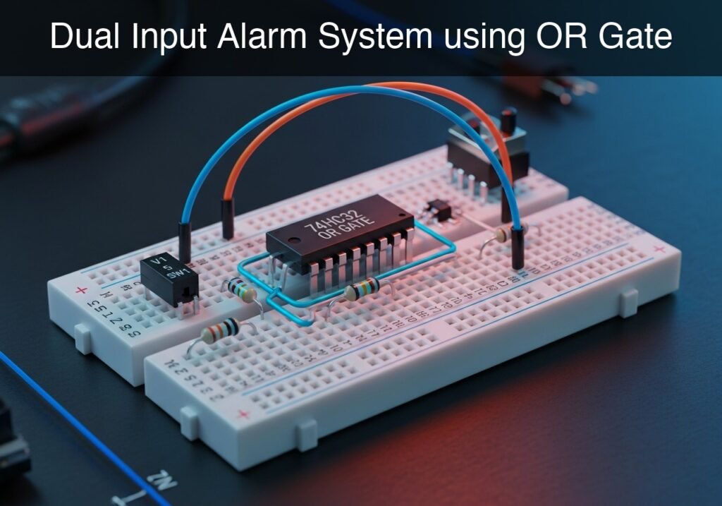
Practical case: Dual Input Alarm System using OR Gate

Dual Input Alarm System using OR Gate prototype (Maker Style)

Level: Basic – Build an alert system that activates a warning LED when either a local or remote signal is triggered.

Objective and use case

In this practical case, you will build a digital alarm indicator utilizing a 74HC32 logic OR gate. The circuit combines two independent input signals (representing a local sensor and a remote sensor) so that if either one or both are activated, the output will drive an alert LED.

Why this circuit is useful:
* Security systems: A single alarm panel can monitor both a front door and a back door.
* Industrial safety: A machine can be halted by either a local emergency stop button or a remote operator console.
* Environmental monitoring: A system can trigger a unified warning if either a smoke detector or a heat sensor detects an anomaly.

Expected outcome:
* With both switches open (0 V at inputs), the output is 0 V and the LED is off.
* Closing the local switch yields 5 V at the first input, forcing the output to 5 V and turning on the LED.
* Closing the remote switch yields 5 V at the second input, forcing the output to 5 V and turning on the LED.
* Closing both switches simultaneously yields 5 V at both inputs, maintaining the 5 V output and keeping the LED illuminated.

Target audience and level: Beginners and hobbyists learning basic digital logic concepts.

Materials

  • U1: 74HC32 quad 2-input OR gate, function: logic control
  • V1: 5 V DC supply, function: power source
  • SW1: SPST switch, function: local alarm trigger
  • SW2: SPST switch, function: remote alarm trigger
  • R1: 10 kΩ resistor, function: pull-down for VA
  • R2: 10 kΩ resistor, function: pull-down for VB
  • R3: 330 Ω resistor, function: LED current limiting
  • D1: red LED, function: alarm indicator

Pin-out of the IC used

74HC32 (Quad 2-input OR gate)

Pin Name Logic function Connection in this case
1 1 A Input 1 for Gate 1 Connects to node VA (from SW1)
2 1B Input 2 for Gate 1 Connects to node VB (from SW2)
3 1Y Output of Gate 1 Connects to node VOUT
7 GND Ground / 0 V reference Connects to node 0
14 VCC Positive supply voltage Connects to node VCC

(Note: Pins 4, 5, 6, 8, 9, 10, 11, 12, and 13 belong to the other three unused OR gates in the package and should ideally have their inputs tied to ground in a permanent design, though they are left out of this primary signal path for simplicity).

Wiring guide

  • V1: Positive terminal connects to node VCC, negative terminal connects to node 0.
  • SW1: Connects between node VCC and node VA.
  • SW2: Connects between node VCC and node VB.
  • R1: Connects between node VA and node 0.
  • R2: Connects between node VB and node 0.
  • U1: Pin 14 connects to node VCC, Pin 7 connects to node 0. Pin 1 connects to node VA, Pin 2 connects to node VB, Pin 3 connects to node VOUT.
  • R3: Connects between node VOUT and node VLED.
  • D1: Anode connects to node VLED, cathode connects to node 0.

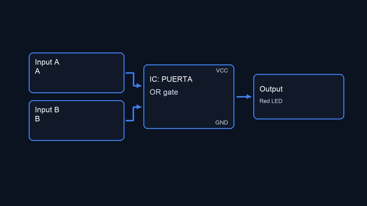
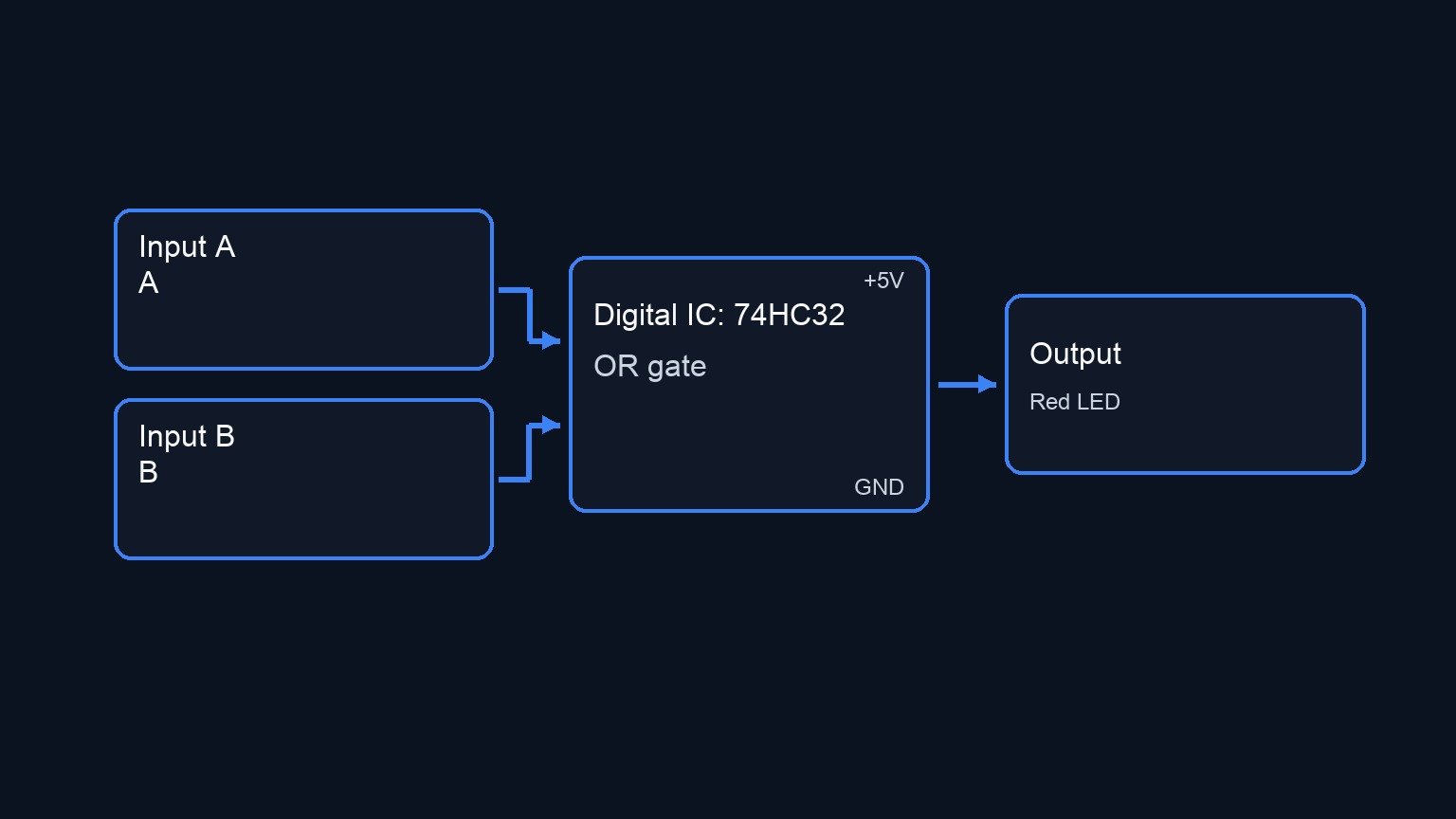
Conceptual block diagram

Conceptual block diagram — PUERTA OR gate
Quick read: inputs → main block → output (actuator or measurement). This summarizes the ASCII schematic below.

Schematic

VCC --> [ SW1: Local Alarm ] --(VA)-->+---------------------------------> [           ]
                                      |                                   [ U1: Pin 1 ]
                                      +--> [ R1: 10 kΩ Pull-down ] --> GND [           ]
                                                                          [  74HC32   ] --(VOUT)--> [ R3: 330 Ω ] --(VLED)--> [ D1: Red LED ] --> GND
VCC --> [ SW2: Remote Alarm] --(VB)-->+---------------------------------> [  OR Gate  ]
                                      |                                   [           ]
                                      +--> [ R2: 10 kΩ Pull-down ] --> GND [ U1: Pin 2 ]
                                                                          [           ]
Electrical Schematic

Truth table

Local Signal (VA) Remote Signal (VB) Output (VOUT) Alarm LED (D1)
0 (Low) 0 (Low) 0 (Low) OFF
0 (Low) 1 (High) 1 (High) ON
1 (High) 0 (Low) 1 (High) ON
1 (High) 1 (High) 1 (High) ON

Measurements and tests

  1. Input Verification: Using a digital multimeter (DMM) referenced to node 0, measure the voltage at nodes VA and VB. Verify that they read approximately 0 V when the respective switch is open, and 5 V when closed.
  2. Output Verification: Measure the voltage at node VOUT. Confirm that it reads 0 V only when both VA and VB are at 0 V. If either or both inputs are at 5 V, VOUT must measure close to 5 V.
  3. Visual Confirmation: Toggle SW1 and SW2 through all four possible combinations as listed in the truth table and confirm D1 behaves accordingly.
  4. Current Measurement (Optional): Place your DMM in series with R3 to measure the LED forward current. It should be approximately 8-10 mA depending on the LED’s forward voltage drop.

SPICE netlist and simulation

Reference SPICE Netlist (ngspice) — excerptFull SPICE netlist (ngspice)

* Dual Input Alarm System using OR Gate
.width out=256

* Power Supply
V1 VCC 0 DC 5

* Local Alarm Trigger (SW1)
* Modeled as a voltage-controlled switch driven by a pulse to simulate user interaction
SW1 VCC VA ctrl1 0 mySW
Vctrl1 ctrl1 0 PULSE(0 5 0 1u 1u 50u 100u)

* Remote Alarm Trigger (SW2)
* Modeled as a voltage-controlled switch driven by a pulse to simulate user interaction
SW2 VCC VB ctrl2 0 mySW
Vctrl2 ctrl2 0 PULSE(0 5 0 1u 1u 100u 200u)

* Switch Model
.model mySW SW(Ron=1 Roff=100Meg Vt=2.5)

* Pull-down resistors
* ... (truncated in public view) ...

Copy this content into a .cir file and run with ngspice.

* Dual Input Alarm System using OR Gate
.width out=256

* Power Supply
V1 VCC 0 DC 5

* Local Alarm Trigger (SW1)
* Modeled as a voltage-controlled switch driven by a pulse to simulate user interaction
SW1 VCC VA ctrl1 0 mySW
Vctrl1 ctrl1 0 PULSE(0 5 0 1u 1u 50u 100u)

* Remote Alarm Trigger (SW2)
* Modeled as a voltage-controlled switch driven by a pulse to simulate user interaction
SW2 VCC VB ctrl2 0 mySW
Vctrl2 ctrl2 0 PULSE(0 5 0 1u 1u 100u 200u)

* Switch Model
.model mySW SW(Ron=1 Roff=100Meg Vt=2.5)

* Pull-down resistors
R1 VA 0 10k
R2 VB 0 10k

* 74HC32 Quad 2-input OR gate (using 1 gate)
XU1 VA VB VOUT 0 VCC U_74HC32_OR

* Robust Subcircuit for 74HC32 OR Gate using continuous math functions
.subckt U_74HC32_OR P1 P2 P3 P7 P14
B1 P3 P7 V = V(P14,P7) * (1 - (1 / (1 + exp(50*(V(P1,P7)-V(P14,P7)/2)))) * (1 / (1 + exp(50*(V(P2,P7)-V(P14,P7)/2)))))
.ends

* Output Indicator
R3 VOUT VLED 330
D1 VLED 0 DLED
.model DLED D(IS=1e-15 N=1.8 RS=10)

* Analysis Commands
.tran 1u 300u
.print tran V(VA) V(VB) V(VOUT) V(VLED)
.op

Simulation Results (Transient Analysis)

Simulation Results (Transient Analysis)
Analysis: The transient analysis spans 0 s to 300 us and captures the switching interval. Main ranges: v(vout) 2.77e-62 uV -> 5 V; v(va) 500 uV -> 5 V; v(vb) 500 uV -> 5 V.
Show raw data table (412 rows)
Index   time            v(va)           v(vb)           v(vout)         v(vled)
0	0.000000e+00	4.999500e-04	4.999500e-04	2.767481e-68	5.488664e-30
1	1.000000e-08	4.999500e-04	4.999500e-04	2.767481e-68	4.008316e-41
2	2.000000e-08	4.999500e-04	4.999500e-04	2.767481e-68	-4.00832e-41
3	4.000000e-08	4.999500e-04	4.999500e-04	2.767481e-68	-1.46362e-51
4	8.000000e-08	4.999500e-04	4.999500e-04	2.767481e-68	5.854466e-52
5	1.600000e-07	4.999500e-04	4.999500e-04	2.767481e-68	3.420369e-62
6	3.200000e-07	4.999500e-04	4.999500e-04	2.767481e-68	-8.55089e-63
7	3.562500e-07	4.999500e-04	4.999500e-04	2.767481e-68	2.767467e-68
8	4.196875e-07	4.999500e-04	4.999500e-04	2.767481e-68	2.767492e-68
9	4.372461e-07	4.999500e-04	4.999500e-04	2.767481e-68	2.767481e-68
10	4.679736e-07	4.999500e-04	4.999500e-04	2.767481e-68	2.767481e-68
11	5.019934e-07	4.999500e+00	4.999500e+00	5.000000e+00	1.503225e+00
12	5.700330e-07	4.999500e+00	4.999500e+00	5.000000e+00	1.502641e+00
13	7.061121e-07	4.999500e+00	4.999500e+00	5.000000e+00	1.502321e+00
14	9.782703e-07	4.999500e+00	4.999500e+00	5.000000e+00	1.502318e+00
15	1.000000e-06	4.999500e+00	4.999500e+00	5.000000e+00	1.502314e+00
16	1.043459e-06	4.999500e+00	4.999500e+00	5.000000e+00	1.502314e+00
17	1.130378e-06	4.999500e+00	4.999500e+00	5.000000e+00	1.502314e+00
18	1.304216e-06	4.999500e+00	4.999500e+00	5.000000e+00	1.502314e+00
19	1.651892e-06	4.999500e+00	4.999500e+00	5.000000e+00	1.502314e+00
20	2.347244e-06	4.999500e+00	4.999500e+00	5.000000e+00	1.502314e+00
21	3.347244e-06	4.999500e+00	4.999500e+00	5.000000e+00	1.502314e+00
22	4.347244e-06	4.999500e+00	4.999500e+00	5.000000e+00	1.502314e+00
23	5.347244e-06	4.999500e+00	4.999500e+00	5.000000e+00	1.502314e+00
... (388 more rows) ...


Reference SPICE netlist (ngspice)

* Dual Input Alarm System using OR Gate
.width out=256

* Power Supply
V1 VCC 0 DC 5

* Local Alarm Trigger (SW1)
* Modeled as a voltage-controlled switch driven by a pulse to simulate user interaction
SW1 VCC VA ctrl1 0 mySW
Vctrl1 ctrl1 0 PULSE(0 5 0 1u 1u 50u 100u)

* Remote Alarm Trigger (SW2)
* Modeled as a voltage-controlled switch driven by a pulse to simulate user interaction
SW2 VCC VB ctrl2 0 mySW
Vctrl2 ctrl2 0 PULSE(0 5 0 1u 1u 100u 200u)

* Switch Model
.model mySW SW(Ron=1 Roff=100Meg Vt=2.5)

* Pull-down resistors
R1 VA 0 10k
R2 VB 0 10k

* 74HC32 Quad 2-input OR gate (using 1 gate)
XU1 VA VB VOUT 0 VCC U_74HC32_OR

* Robust Subcircuit for 74HC32 OR Gate using continuous math functions
.subckt U_74HC32_OR P1 P2 P3 P7 P14
B1 P3 P7 V = V(P14,P7) * (1 - (1 / (1 + exp(50*(V(P1,P7)-V(P14,P7)/2)))) * (1 / (1 + exp(50*(V(P2,P7)-V(P14,P7)/2)))))
.ends

* Output Indicator
R3 VOUT VLED 330
D1 VLED 0 DLED
.model DLED D(IS=1e-15 N=1.8 RS=10)

* Analysis Commands
.tran 1u 300u
.print tran V(VA) V(VB) V(VOUT) V(VLED)
.op

Simulation Results (Transient Analysis)

Simulation Results (Transient Analysis)
Analysis: The transient analysis spans 0 s to 300 us and captures the switching interval. Main ranges: v(vout) 2.77e-62 uV -> 5 V; v(va) 500 uV -> 5 V; v(vb) 500 uV -> 5 V.

Common mistakes and how to avoid them

  1. Floating inputs: Forgetting to connect the pull-down resistors (R1 and R2). Without them, when the switches are open, the 74HC32 inputs act like antennas and will cause the output to randomly toggle or oscillate. Always use pull-down resistors.
  2. Missing LED current limiting resistor: Connecting the LED directly from the output pin (node VOUT) to ground. This will draw excessive current, potentially burning out both the LED and the 74HC32 output stage. Always include R3.
  3. Forgetting IC power connections: Wiring the inputs and outputs but forgetting to supply VCC to pin 14 and GND to pin 7. The IC cannot function without its power rails connected.


Troubleshooting

  • Symptom: The LED is always ON, regardless of switch positions.
    • Cause: Inputs are permanently shorted to VCC, or switches are wired as «Normally Closed».
    • Fix: Verify that the switches only bridge VCC to the inputs when actively pressed. Ensure nodes VA and VB measure 0 V when switches are released.
  • Symptom: The LED never turns ON.
    • Cause: LED D1 is inserted backwards (reversed polarity), or the IC is not powered.
    • Fix: Check the orientation of D1 (anode to R3, cathode to ground). Measure pin 14 on U1 to guarantee it receives 5 V.
  • Symptom: The LED flickers when you move your hand near the circuit.
    • Cause: The inputs are floating. CMOS chips have highly sensitive inputs.
    • Fix: Check the connections of R1 and R2. Ensure they securely tie nodes VA and VB to ground when the switches are open.

Possible improvements and extensions

  1. Audible alert integration: Add an active 5 V piezoelectric buzzer in parallel with the LED/resistor combination (connecting the buzzer’s positive lead to VOUT and the negative lead to node 0) to provide both a visual and audible alarm.
  2. Expand to a 3-input alarm: Utilize a second OR gate inside the same 74HC32 chip. Connect VOUT to Pin 4 (2 A), a third switch/pull-down assembly to Pin 5 (2B), and use Pin 6 (2Y) to drive the LED, creating a system that monitors three distinct zones.

More Practical Cases on Prometeo.blog

Find this product and/or books on this topic on Amazon

Go to Amazon

As an Amazon Associate, I earn from qualifying purchases. If you buy through this link, you help keep this project running.

Quick Quiz

Question 1: What is the main logic gate used in this alert system?


Question 2: What condition turns the warning LED off?


Question 3: What voltage represents an open switch at the inputs in this circuit?


Question 4: What happens to the LED if only the local switch is closed?


Question 5: Which of the following is a mentioned use case for this circuit?


Question 6: In the environmental monitoring example, what two sensors are combined?


Question 7: What is the output voltage when both switches are closed simultaneously?


Question 8: How many independent input signals does this specific circuit combine?


Question 9: What does the output of the 74HC32 gate drive in this practical case?


Question 10: In a security system application, what could the two inputs represent?


Carlos Núñez Zorrilla
Electronics & Computer Engineer

Telecommunications Electronics Engineer and Computer Engineer (official degrees in Spain).
Follow me:


Practical case: Nurse call bell

Nurse call bell prototype (Maker Style)

Level: Basic – Implement an OR gate to activate an alert from two independent switches.

Objective and use case

You will build a basic nurse call circuit using a digital OR gate to trigger a visual alert whenever either of two patient bed switches is pressed.

Why it is useful:
* Allows centralized monitoring of multiple independent trigger points.
* Demonstrates how basic digital logic simplifies parallel alarm systems without cross-wiring physical switches.
* Forms the foundation for larger, more complex call bell or security systems.

Expected outcome:
* Pressing switch A drives the output HIGH (near 5 V), lighting the LED.
* Pressing switch B drives the output HIGH (near 5 V), lighting the LED.
* Pressing both switches simultaneously drives the output HIGH, lighting the LED.
* The output remains LOW (0 V) and the LED stays off when no switches are pressed.

Target audience and level: Beginners learning digital logic gates and the importance of pull-down networks.

Materials

  • V1: 5 V DC supply
  • U1: 74HC32 quad 2-input OR gate IC
  • SW1: Push button switch, normally open, function: Bed A trigger
  • SW2: Push button switch, normally open, function: Bed B trigger
  • R1: 10 kΩ resistor, function: pull-down for VA
  • R2: 10 kΩ resistor, function: pull-down for VB
  • R3: 330 Ω resistor, function: LED current limiting
  • D1: Red LED, function: alert indicator

Pin-out of the IC used

74HC32 (Quad 2-Input OR Gate)

Pin Name Logic function Connection in this case
1 1 A Input 1 for Gate 1 Node VA (Switch A)
2 1B Input 2 for Gate 1 Node VB (Switch B)
3 1Y Output of Gate 1 Node VOUT (to LED circuit)
7 GND Ground Node 0
14 VCC Power Supply Node VCC

(Note: Pins 4, 5, 8, 9, 10, 11, 12, 13 are unused inputs and should be tied to Ground in a permanent circuit to prevent CMOS latch-up).

Wiring guide

  • V1: positive terminal connects to VCC; negative terminal connects to 0.
  • SW1: connects between VCC and VA.
  • SW2: connects between VCC and VB.
  • R1: connects between VA and 0.
  • R2: connects between VB and 0.
  • U1 (pin 14): connects to VCC.
  • U1 (pin 7): connects to 0.
  • U1 (pin 1): connects to VA.
  • U1 (pin 2): connects to VB.
  • U1 (pin 3): connects to VOUT.
  • R3: connects between VOUT and the anode of D1.
  • D1: cathode connects to 0.

Conceptual block diagram

Conceptual block diagram — 74HC32 OR gate
Quick read: inputs → main block → output (actuator or measurement). This summarizes the ASCII schematic below.

Schematic

VCC --> [ SW1: Bed A ] --(VA)--> [ R1: 10 kΩ Pull-down ] --> GND
                             \
                              -->(Pin 1) \
                                          [ U1: 74HC32 OR Gate ] --(VOUT, Pin 3)--> [ R3: 330 Ω ] --> [ D1: Red LED ] --> GND
                                          /
                              -->(Pin 2) /
                             /
VCC --> [ SW2: Bed B ] --(VB)--> [ R2: 10 kΩ Pull-down ] --> GND
Electrical Schematic

Truth table

Input A (VA) Input B (VB) Output Y (VOUT) LED State
0 (LOW) 0 (LOW) 0 (LOW) OFF
0 (LOW) 1 (HIGH) 1 (HIGH) ON
1 (HIGH) 0 (LOW) 1 (HIGH) ON
1 (HIGH) 1 (HIGH) 1 (HIGH) ON

Measurements and tests

  1. Power Verification: Measure the voltage between VCC and 0 using a multimeter to ensure it is exactly 5 V.
  2. Idle State Testing: Without pressing any buttons, measure the voltage at nodes VA and VB. Both should read exactly 0 V. The node VOUT should also read 0 V.
  3. Logic HIGH Testing: Press and hold SW1. Measure node VA (should be ~5 V) and measure node VOUT (should be ~5 V). Verify the LED is ON. Repeat this process for SW2 and node VB.
  4. Current Measurement (Optional): Place your multimeter in series with R3 and D1 to measure the forward current of the LED (it should be roughly 8-10 mA depending on the LED’s forward voltage drop).

SPICE netlist and simulation

Reference SPICE Netlist (ngspice) — excerptFull SPICE netlist (ngspice)

* Practical case: Nurse call bell
.width out=256

* Power Supply
V1 VCC 0 DC 5

* Bed A Trigger (SW1)
* Modeled as a voltage-controlled switch activated by a pulse to simulate a user pressing the button
VctrlA ctrlA 0 PULSE(0 5 10u 1u 1u 40u 100u)
S1 VCC VA ctrlA 0 my_switch

* Bed B Trigger (SW2)
* Modeled as a voltage-controlled switch activated by a pulse to simulate a user pressing the button
VctrlB ctrlB 0 PULSE(0 5 10u 1u 1u 90u 200u)
S2 VCC VB ctrlB 0 my_switch

* Pull-down resistors for switch inputs
R1 VA 0 10k
R2 VB 0 10k

* ... (truncated in public view) ...

Copy this content into a .cir file and run with ngspice.

* Practical case: Nurse call bell
.width out=256

* Power Supply
V1 VCC 0 DC 5

* Bed A Trigger (SW1)
* Modeled as a voltage-controlled switch activated by a pulse to simulate a user pressing the button
VctrlA ctrlA 0 PULSE(0 5 10u 1u 1u 40u 100u)
S1 VCC VA ctrlA 0 my_switch

* Bed B Trigger (SW2)
* Modeled as a voltage-controlled switch activated by a pulse to simulate a user pressing the button
VctrlB ctrlB 0 PULSE(0 5 10u 1u 1u 90u 200u)
S2 VCC VB ctrlB 0 my_switch

* Pull-down resistors for switch inputs
R1 VA 0 10k
R2 VB 0 10k

* U1: 74HC32 quad 2-input OR gate IC (using 1 gate)
* Wiring: Pin 1 -> VA, Pin 2 -> VB, Pin 3 -> VOUT, Pin 14 -> VCC, Pin 7 -> 0
XU1 VA VB VOUT VCC 0 74HC32_OR

* Alert Indicator (LED and current limiting resistor)
R3 VOUT D1_A 330
D1 D1_A 0 DLED

* --- Models and Subcircuits ---

* Ideal switch model
.model my_switch SW(vt=2.5 vh=0.5 ron=1 roff=100MEG)

* Generic Red LED model
.model DLED D(IS=1e-20 N=2.2 RS=2)

* Behavioral model for a 74HC32 OR gate (Continuous functions for robust convergence)
.subckt 74HC32_OR A B Y VCC GND
RinA A GND 10MEG
RinB B GND 10MEG
* OR Logic: V_out = VCC * (1 - (1-A)*(1-B)) implemented with sigmoids
B1 Y_int GND V = V(VCC) * (1 - (1 - 1/(1+exp(-50*(V(A)-2.5)))) * (1 - 1/(1+exp(-50*(V(B)-2.5)))))
Rout Y_int Y 10
.ends

* --- Analysis Directives ---

.tran 1u 250u
.print tran V(VA) V(VB) V(VOUT) V(D1_A)
.op
.end

Simulation Results (Transient Analysis)

Simulation Results (Transient Analysis)
Analysis: The transient analysis spans 0 s to 250 us and captures the switching interval. Main ranges: v(vout) -1.01e-29 uV -> 4.92 V; v(va) 499 uV -> 5 V; v(vb) 499 uV -> 5 V.
Show raw data table (354 rows)
Index   time            v(va)           v(vb)           v(vout)         v(d1_a)
0	0.000000e+00	4.994506e-04	4.994506e-04	-1.00582e-35	-3.41977e-34
1	1.000000e-08	4.994506e-04	4.994506e-04	-6.04520e-52	-2.05537e-50
2	2.000000e-08	4.994506e-04	4.994506e-04	6.045198e-52	2.055367e-50
3	4.000000e-08	4.994506e-04	4.994506e-04	1.816637e-67	6.176631e-66
4	8.000000e-08	4.994506e-04	4.994506e-04	-7.26682e-68	-2.47066e-66
5	1.600000e-07	4.994506e-04	4.994506e-04	-1.94609e-72	-1.94609e-72
6	3.200000e-07	4.994506e-04	4.994506e-04	-1.94609e-72	-1.94609e-72
7	6.400000e-07	4.994506e-04	4.994506e-04	-1.94609e-72	-1.94609e-72
8	1.280000e-06	4.994506e-04	4.994506e-04	-1.94609e-72	-1.94609e-72
9	2.280000e-06	4.994506e-04	4.994506e-04	-1.94609e-72	-1.94609e-72
10	3.280000e-06	4.994506e-04	4.994506e-04	-1.94609e-72	-1.94609e-72
11	4.280000e-06	4.994506e-04	4.994506e-04	-1.94609e-72	-1.94609e-72
12	5.280000e-06	4.994506e-04	4.994506e-04	-1.94609e-72	-1.94609e-72
13	6.280000e-06	4.994506e-04	4.994506e-04	-1.94609e-72	-1.94609e-72
14	7.280000e-06	4.994506e-04	4.994506e-04	-1.94609e-72	-1.94609e-72
15	8.280000e-06	4.994506e-04	4.994506e-04	-1.94609e-72	-1.94609e-72
16	9.280000e-06	4.994506e-04	4.994506e-04	-1.94609e-72	-1.94609e-72
17	1.000000e-05	4.994506e-04	4.994506e-04	-1.94609e-72	-1.94609e-72
18	1.010000e-05	4.994506e-04	4.994506e-04	-1.94609e-72	-1.94609e-72
19	1.030000e-05	4.994506e-04	4.994506e-04	-1.94609e-72	-1.94609e-72
20	1.035875e-05	4.994506e-04	4.994506e-04	-1.94609e-72	-1.94609e-72
21	1.046156e-05	4.994506e-04	4.994506e-04	-1.94609e-72	-1.94609e-72
22	1.049002e-05	4.994506e-04	4.994506e-04	-1.94609e-72	-1.94609e-72
23	1.053982e-05	4.994506e-04	4.994506e-04	-1.94609e-72	-1.94609e-72
... (330 more rows) ...


Reference SPICE netlist (ngspice)

* Practical case: Nurse call bell
.width out=256

* Power Supply
V1 VCC 0 DC 5

* Bed A Trigger (SW1)
* Modeled as a voltage-controlled switch activated by a pulse to simulate a user pressing the button
VctrlA ctrlA 0 PULSE(0 5 10u 1u 1u 40u 100u)
S1 VCC VA ctrlA 0 my_switch

* Bed B Trigger (SW2)
* Modeled as a voltage-controlled switch activated by a pulse to simulate a user pressing the button
VctrlB ctrlB 0 PULSE(0 5 10u 1u 1u 90u 200u)
S2 VCC VB ctrlB 0 my_switch

* Pull-down resistors for switch inputs
R1 VA 0 10k
R2 VB 0 10k

* U1: 74HC32 quad 2-input OR gate IC (using 1 gate)
* Wiring: Pin 1 -> VA, Pin 2 -> VB, Pin 3 -> VOUT, Pin 14 -> VCC, Pin 7 -> 0
XU1 VA VB VOUT VCC 0 74HC32_OR

* Alert Indicator (LED and current limiting resistor)
R3 VOUT D1_A 330
D1 D1_A 0 DLED

* --- Models and Subcircuits ---

* Ideal switch model
.model my_switch SW(vt=2.5 vh=0.5 ron=1 roff=100MEG)

* Generic Red LED model
.model DLED D(IS=1e-20 N=2.2 RS=2)

* Behavioral model for a 74HC32 OR gate (Continuous functions for robust convergence)
.subckt 74HC32_OR A B Y VCC GND
RinA A GND 10MEG
RinB B GND 10MEG
* OR Logic: V_out = VCC * (1 - (1-A)*(1-B)) implemented with sigmoids
B1 Y_int GND V = V(VCC) * (1 - (1 - 1/(1+exp(-50*(V(A)-2.5)))) * (1 - 1/(1+exp(-50*(V(B)-2.5)))))
Rout Y_int Y 10
.ends

* --- Analysis Directives ---

.tran 1u 250u
.print tran V(VA) V(VB) V(VOUT) V(D1_A)
.op
.end

Simulation Results (Transient Analysis)

Simulation Results (Transient Analysis)
Analysis: The transient analysis spans 0 s to 250 us and captures the switching interval. Main ranges: v(vout) -1.01e-29 uV -> 4.92 V; v(va) 499 uV -> 5 V; v(vb) 499 uV -> 5 V.

Common mistakes and how to avoid them

  • Floating inputs: Forgetting the pull-down resistors (R1 and R2). Without them, the voltage at the gate inputs will float when the switches are open, causing random, unpredictable triggering of the alarm.
  • Omitting power connections to the IC: Forgetting to connect pins 7 and 14 to Ground and VCC, respectively. The logic gate cannot function without its own power supply.
  • Leaving unused CMOS inputs floating: The 74HC32 is a CMOS device. Any unused input pins (e.g., pins 4, 5, 9, 10, 12, 13) should be tied to Ground (0) to prevent excess power consumption or erratic behavior.


Troubleshooting

  • Symptom: The LED stays ON constantly, even when no buttons are pressed.
  • Cause: One of the pull-down resistors (R1 or R2) is missing or not properly connected to ground.
  • Fix: Verify the connection of the resistors between inputs VA or VB and node 0.
  • Symptom: The LED never turns ON.
  • Cause: LED is installed backward, missing VCC/GND to the IC, or a disconnected R3.
  • Fix: Check LED polarity (flat side / shorter leg goes to node 0). Ensure pins 7 and 14 on U1 have power.
  • Symptom: The LED turns ON randomly when my hand is near the breadboard.
  • Cause: The circuit is experiencing a «floating input» acting as an antenna picking up stray capacitance.
  • Fix: Check your pull-down resistors. Make sure they firmly connect the input pins to ground.
  • Symptom: Output is logic HIGH (measured at pin 3), but LED is extremely dim.
  • Cause: The current limiting resistor R3 is too large (e.g., 10 kΩ instead of 330 Ω).
  • Fix: Replace R3 with the correct 330 Ω value.

Possible improvements and extensions

  • Add an audible alert: Connect an active 5 V buzzer in parallel with the LED/resistor combination so that triggering the switch produces both a light and a sound.
  • Implement a latching circuit: In a real hospital, the light must stay ON until a nurse arrives to reset it. Feed the output of the OR gate into the SET pin of an SR Latch (or use logic gates to build one), and add a third «Reset» button at the nurse station.

More Practical Cases on Prometeo.blog

Find this product and/or books on this topic on Amazon

Go to Amazon

As an Amazon Associate, I earn from qualifying purchases. If you buy through this link, you help keep this project running.

Quick Quiz

Question 1: What is the main objective of the circuit described in the article?


Question 2: Which type of digital logic gate is used to trigger the visual alert in this circuit?


Question 3: What happens to the output when neither switch is pressed?


Question 4: What is the expected outcome if both patient bed switches are pressed simultaneously?


Question 5: Which IC model is used as the quad 2-input OR gate in this project?


Question 6: Which IC model is used as the quad 2-input OR gate in this project?


Question 7: Which IC model is used as the quad 2-input OR gate in this project?


Question 8: Which IC model is used as the quad 2-input OR gate in this project?


Question 9: Which IC model is used as the quad 2-input OR gate in this project?


Question 10: Which IC model is used as the quad 2-input OR gate in this project?


Carlos Núñez Zorrilla
Electronics & Computer Engineer

Telecommunications Electronics Engineer and Computer Engineer (official degrees in Spain).
Follow me:


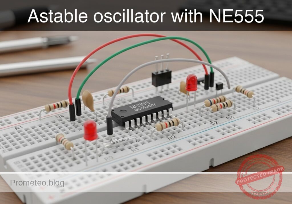
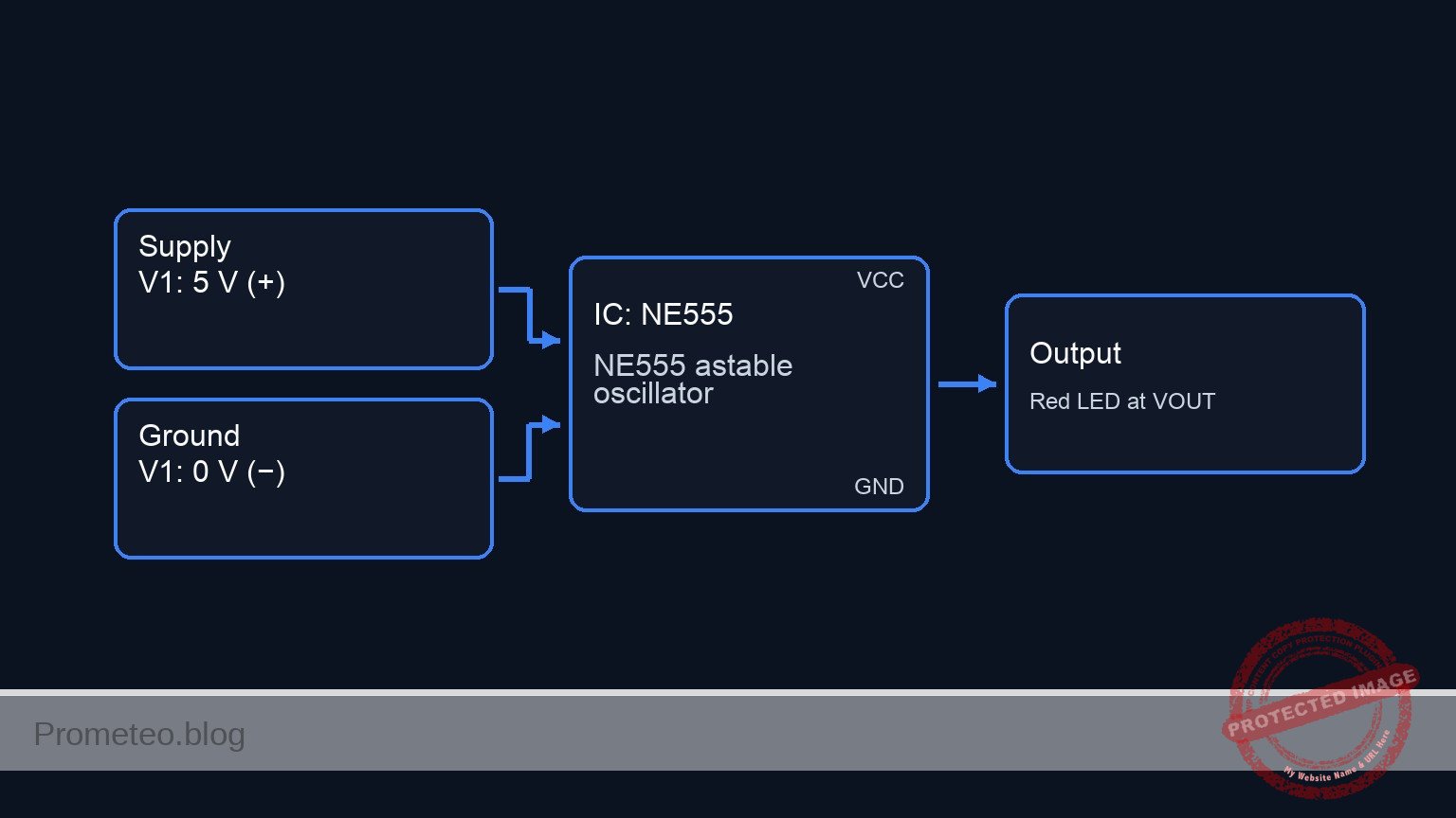
Practical case: astable oscillator with NE555

Astable oscillator with NE555 prototype (Maker Style)

Level: Basic — Build an NE555 astable timer that blinks an LED at a visible frequency.

Objective and use case

You will build a simple astable timer with an NE555 powered from 5 V. The circuit will generate a repetitive square wave that turns an LED on and off continuously.

Why it is useful:
– It demonstrates how a basic timer generates a clock signal without a microcontroller.
– It is useful as a visual blink indicator for power or system status.
– It can be used as a simple test source for checking frequency measurement tools.
– It helps students observe capacitor charge and discharge behavior in a real circuit.

Expected outcome:
VOUT switches between approximately 0 V and 5 V.
– The LED blinks at a clearly visible rate, about 1 Hz to 3 Hz.
– The timing node TH_TR shows a repeating charge/discharge waveform between about 1/3 VCC and 2/3 VCC.
– The measured period is close to the value predicted by the NE555 astable equations.
– The duty cycle is greater than 50% for the standard RA/RB astable connection.

Target audience and level: Beginners in basic electronics laboratory practice.

Materials

  • U1: NE555 timer IC, function: astable oscillator core
  • R1: 10 kΩ resistor, function: timing resistor RA from VCC to DIS
  • R2: 68 kΩ resistor, function: timing resistor RB from DIS to TH_TR
  • C1: 10 µF electrolytic capacitor, function: timing capacitor
  • C2: 10 nF capacitor, function: control-voltage noise filter on CV
  • C3: 100 nF capacitor, function: supply decoupling across VCC and GND
  • R3: 330 Ω resistor, function: LED current limiting
  • D1: red LED, function: visual output indicator
  • V1: 5 V DC supply
  • B1: breadboard, function: circuit assembly platform
  • J1: jumper wires, function: interconnections

Wiring guide

Use the node names VCC, 0, DIS, TH_TR, CV, RESET, and VOUT.

  • V1 connects between nodes VCC and 0.
  • U1 pin 8 (VCC) connects to node VCC.
  • U1 pin 1 (GND) connects to node 0.
  • U1 pin 4 (RESET) connects to node VCC.
  • U1 pin 3 (OUT) connects to node VOUT.
  • U1 pin 7 (DISCH) connects to node DIS.
  • U1 pin 2 (TRIG) connects to node TH_TR.
  • U1 pin 6 (THRESH) connects to node TH_TR.
  • U1 pin 5 (CTRL) connects to node CV.
  • R1 connects between nodes VCC and DIS.
  • R2 connects between nodes DIS and TH_TR.
  • C1 connects between nodes TH_TR and 0; if electrolytic, connect the positive lead to TH_TR and the negative lead to 0.
  • C2 connects between nodes CV and 0.
  • C3 connects between nodes VCC and 0, placed physically close to U1.
  • R3 connects between nodes VOUT and LED_A.
  • D1 connects between nodes LED_A and 0; connect the anode to LED_A and the cathode to 0.

Conceptual block diagram

Conceptual block diagram — NE555 NE555 astable oscillator
Quick read: inputs → main block → output (actuator or measurement). This summarizes the ASCII schematic below.

Schematic

Practical case: astable oscillator with NE555

[ V1: 5 V DC ] --(+)--> [ VCC ]
[ V1: 5 V DC ] --(-)--> [ 0 ]

[ VCC ] --(pin8 supply)--> [ U1: NE555 astable core ] --(pin3 = VOUT)--> [ R3: 330 ohm ] --(LED_A)--> [ D1: Red LED ] --> [ 0 ]
[ VCC ] --(RESET to pin4)--> [ U1: NE555 astable core ]
[ VCC ] --(R1: 10 k ohm, RA)--> [ DIS / U1 pin7 ] --(R2: 68 k ohm, RB)--> [ TH_TR / U1 pins2+6 ] --(timing sense)--> [ U1: NE555 astable core ]
[ TH_TR / U1 pins2+6 ] --(C1: 10 uF, + to TH_TR, - to 0)--> [ 0 ]
[ U1 pin5 = CV ] --(C2: 10 nF noise filter to 0)--> [ 0 ]
[ VCC ] --(C3: 100 nF decoupling to 0, close to U1)--> [ 0 ]
[ U1 pin1 = GND ] --> [ 0 ]
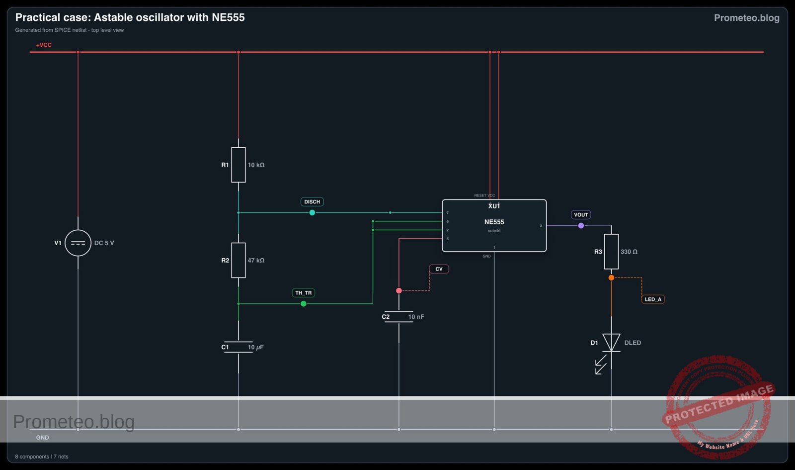
Electrical Schematic

Electrical diagram

Electrical diagram for case: Practical case: astable oscillator with NE555
Generated from the validated SPICE netlist for this case.

🔒 This electrical diagram is premium. With the monthly membership (7-day free trial) you can unlock the complete didactic material and the print-ready PDF pack.🔓 See premium access plans

Measurements and tests

  1. Power-off inspection
  2. Check that U1 pin 1 goes to 0 and U1 pin 8 goes to VCC.
  3. Verify that U1 pin 2 and U1 pin 6 are linked together at TH_TR.
  4. Confirm LED polarity: anode toward R3, cathode toward 0.

  5. Initial power test

  6. Apply 5 V from V1.
  7. The LED should start blinking immediately.
  8. If the LED stays always on or always off, remove power and recheck wiring.

  9. Measure output voltage

  10. Probe VOUT with a multimeter or oscilloscope.
  11. With an oscilloscope, expect a square-like waveform from near 0 V to near 5 V.
  12. With a multimeter, the reading may show an average voltage between these limits, depending on blink speed.

  13. Measure the timing node

  14. Probe TH_TR.
  15. Expect a repeating capacitor waveform rising from about 1.67 V to 3.33 V when VCC = 5 V.
  16. This confirms the internal 1/3 VCC and 2/3 VCC thresholds of the NE555.

  17. Check the control-voltage node

  18. Probe CV.
  19. Expect a nearly steady voltage close to 2/3 VCC, around 3.3 V, with small ripple.

  20. Estimate period and frequency

  21. Use the standard astable equations:
  22. T = 0.693 x (R1 + 2R2) x C1
  23. f = 1 / T
  24. With R1 = 10 kΩ, R2 = 68 kΩ, C1 = 10 µF:
  25. T ≈ 0.693 x (10k + 136k) x 10 µF ≈ 1.01 s
  26. f ≈ 0.99 Hz
  27. Measured blinking should be close to 1 blink per second.

  28. Estimate duty cycle

  29. Use:
  30. tHIGH = 0.693 x (R1 + R2) x C1
  31. tLOW = 0.693 x R2 x C1
  32. Duty cycle ≈ tHIGH / T
  33. For these values, duty cycle is about 53%.
  34. On the oscilloscope, the high time should be slightly longer than the low time.

SPICE netlist and simulation

Reference SPICE Netlist (ngspice) — excerptFull SPICE netlist (ngspice)

* Practical case: Astable oscillator with NE555
.width out=256

* Power Supply
V1 VCC 0 DC 5

* NE555 Timer IC Subcircuit Instance
* Pins: GND TRIG OUT RESET CTRL THRES DISCH VCC_PIN
XU1 0 TH_TR VOUT VCC CV TH_TR DISCH VCC NE555

* Timing Components
R1 VCC DISCH 10k
R2 DISCH TH_TR 47k
C1 TH_TR 0 10u
C2 CV 0 10n

* Output Load (LED)
R3 VOUT LED_A 330
D1 LED_A 0 DLED

* ... (truncated in public view) ...

Copy this content into a .cir file and run with ngspice.

🔒 Part of this section is premium. With the monthly membership (7-day free trial) you can access the full content (materials, wiring, detailed build, validation, troubleshooting, variants and checklist) and download the complete print-ready PDF pack.

* Practical case: Astable oscillator with NE555
.width out=256

* Power Supply
V1 VCC 0 DC 5

* NE555 Timer IC Subcircuit Instance
* Pins: GND TRIG OUT RESET CTRL THRES DISCH VCC_PIN
XU1 0 TH_TR VOUT VCC CV TH_TR DISCH VCC NE555

* Timing Components
R1 VCC DISCH 10k
R2 DISCH TH_TR 47k
C1 TH_TR 0 10u
C2 CV 0 10n

* Output Load (LED)
R3 VOUT LED_A 330
D1 LED_A 0 DLED

* Models
.MODEL DLED D(IS=1e-19 N=1.6 RS=10 BV=5 IBV=10u)

* Behavioral NE555 Subcircuit
.SUBCKT NE555 GND TRIG OUT RESET CTRL THRES DISCH VCC_PIN
* Internal voltage divider (3 x 5k resistors)
R1 VCC_PIN CTRL 5k
R2 CTRL N1 5k
R3 N1 GND 5k

* Smooth comparators for threshold, trigger, and reset
B_COMP_TH COMP_TH GND V=0.5*(1+tanh(100*(V(THRES,GND)-V(CTRL,GND))))
B_COMP_TR COMP_TR GND V=0.5*(1+tanh(100*(V(N1,GND)-V(TRIG,GND))))
B_COMP_RST COMP_RST GND V=0.5*(1+tanh(100*(0.7-V(RESET,GND))))

* SR Latch (Integrator with positive feedback for infinite hold time)
B_LATCH GND LATCH I=V(COMP_TR,GND) - V(COMP_TH,GND) - 5*V(COMP_RST,GND) + (V(LATCH,GND)>0.5 ? 0.1 : -0.1)
C_LATCH LATCH GND 1n
R_LATCH LATCH GND 100Meg

* Latch Voltage Clamps (Clamps V(LATCH) between ~0V and ~1V)
D1 GND LATCH D_CLAMP
V_CLAMP V_CLAMP_NODE GND 1
D2 LATCH V_CLAMP_NODE D_CLAMP
.model D_CLAMP D(N=0.01 RS=1)

* Output Driver Stage
B_OUT OUT_INT GND V=V(LATCH,GND)>0.5 ? V(VCC_PIN,GND) : 0.1
R_OUT OUT_INT OUT 10

* Open-Collector Discharge Transistor (Modeled as a Switch)
B_DISCH_CTRL DISCH_CTRL GND V=V(LATCH,GND)<0.5 ? 1 : 0
S_DISCH DISCH GND DISCH_CTRL GND SW_DISCH
.model SW_DISCH SW(VT=0.5 RON=15 ROFF=100Meg)
.ENDS

* Force initial condition on timing capacitor to ensure guaranteed oscillator startup
.ic V(TH_TR)=0

* Simulation Commands
.op
.tran 1m 3
.print tran V(VOUT) V(TH_TR) V(DISCH) V(LED_A) V(CV)

Simulation Results (Transient Analysis)

Simulation Results (Transient Analysis)
Analysis: The transient analysis spans 0 s to 3 s. Main ranges: v(vout) 100 mV -> 4.9 V; v(disch) 8.02 mV -> 4.71 V; v(th_tr) 0 uV -> 3.32 V.
Show raw data table (3013 rows)
Index   time            v(vout)         v(th_tr)        v(disch)        v(led_a)        v(cv)
0	0.000000e+00	4.903386e+00	0.000000e+00	4.122467e+00	1.715117e+00	3.333333e+00
1	1.000000e-05	4.903386e+00	8.771053e-05	4.122482e+00	1.715117e+00	3.333333e+00
2	2.000000e-05	4.903386e+00	1.754195e-04	4.122498e+00	1.715117e+00	3.333333e+00
3	4.000000e-05	4.903386e+00	3.508344e-04	4.122529e+00	1.715117e+00	3.333333e+00
4	8.000000e-05	4.903386e+00	7.016457e-04	4.122590e+00	1.715117e+00	3.333333e+00
5	1.600000e-04	4.903386e+00	1.403195e-03	4.122713e+00	1.715117e+00	3.333333e+00
6	3.200000e-04	4.903386e+00	2.805997e-03	4.122959e+00	1.715117e+00	3.333333e+00
7	6.400000e-04	4.903386e+00	5.610420e-03	4.123451e+00	1.715117e+00	3.333333e+00
8	1.280000e-03	4.903386e+00	1.121455e-02	4.124434e+00	1.715117e+00	3.333333e+00
9	2.280000e-03	4.903386e+00	1.995841e-02	4.125968e+00	1.715117e+00	3.333333e+00
10	3.280000e-03	4.903386e+00	2.868694e-02	4.127499e+00	1.715117e+00	3.333333e+00
11	4.280000e-03	4.903386e+00	3.740018e-02	4.129028e+00	1.715117e+00	3.333333e+00
12	5.280000e-03	4.903386e+00	4.609814e-02	4.130554e+00	1.715117e+00	3.333333e+00
13	6.280000e-03	4.903386e+00	5.478085e-02	4.132077e+00	1.715117e+00	3.333333e+00
14	7.280000e-03	4.903386e+00	6.344835e-02	4.133597e+00	1.715117e+00	3.333333e+00
15	8.280000e-03	4.903386e+00	7.210065e-02	4.135115e+00	1.715117e+00	3.333333e+00
16	9.280000e-03	4.903386e+00	8.073778e-02	4.136630e+00	1.715117e+00	3.333333e+00
17	1.028000e-02	4.903386e+00	8.935978e-02	4.138143e+00	1.715117e+00	3.333333e+00
18	1.128000e-02	4.903386e+00	9.796666e-02	4.139653e+00	1.715117e+00	3.333333e+00
19	1.228000e-02	4.903386e+00	1.065585e-01	4.141160e+00	1.715117e+00	3.333333e+00
20	1.328000e-02	4.903386e+00	1.151352e-01	4.142665e+00	1.715117e+00	3.333333e+00
21	1.428000e-02	4.903386e+00	1.236969e-01	4.144166e+00	1.715117e+00	3.333333e+00
22	1.528000e-02	4.903386e+00	1.322436e-01	4.145666e+00	1.715117e+00	3.333333e+00
23	1.628000e-02	4.903386e+00	1.407753e-01	4.147162e+00	1.715117e+00	3.333333e+00
... (2989 more rows) ...


Reference SPICE netlist (ngspice)

* Practical case: Astable oscillator with NE555
.width out=256

* Power Supply
V1 VCC 0 DC 5

* NE555 Timer IC Subcircuit Instance
* Pins: GND TRIG OUT RESET CTRL THRES DISCH VCC_PIN
XU1 0 TH_TR VOUT VCC CV TH_TR DISCH VCC NE555

* Timing Components
R1 VCC DISCH 10k
R2 DISCH TH_TR 47k
C1 TH_TR 0 10u
C2 CV 0 10n

* Output Load (LED)
R3 VOUT LED_A 330
D1 LED_A 0 DLED

* Models
.MODEL DLED D(IS=1e-19 N=1.6 RS=10 BV=5 IBV=10u)

* Behavioral NE555 Subcircuit
.SUBCKT NE555 GND TRIG OUT RESET CTRL THRES DISCH VCC_PIN
* Internal voltage divider (3 x 5k resistors)
R1 VCC_PIN CTRL 5k
R2 CTRL N1 5k
R3 N1 GND 5k

* Smooth comparators for threshold, trigger, and reset
B_COMP_TH COMP_TH GND V=0.5*(1+tanh(100*(V(THRES,GND)-V(CTRL,GND))))
B_COMP_TR COMP_TR GND V=0.5*(1+tanh(100*(V(N1,GND)-V(TRIG,GND))))
B_COMP_RST COMP_RST GND V=0.5*(1+tanh(100*(0.7-V(RESET,GND))))

* SR Latch (Integrator with positive feedback for infinite hold time)
B_LATCH GND LATCH I=V(COMP_TR,GND) - V(COMP_TH,GND) - 5*V(COMP_RST,GND) + (V(LATCH,GND)>0.5 ? 0.1 : -0.1)
C_LATCH LATCH GND 1n
R_LATCH LATCH GND 100Meg

* Latch Voltage Clamps (Clamps V(LATCH) between ~0V and ~1V)
D1 GND LATCH D_CLAMP
V_CLAMP V_CLAMP_NODE GND 1
D2 LATCH V_CLAMP_NODE D_CLAMP
.model D_CLAMP D(N=0.01 RS=1)

* Output Driver Stage
B_OUT OUT_INT GND V=V(LATCH,GND)>0.5 ? V(VCC_PIN,GND) : 0.1
R_OUT OUT_INT OUT 10

* Open-Collector Discharge Transistor (Modeled as a Switch)
B_DISCH_CTRL DISCH_CTRL GND V=V(LATCH,GND)<0.5 ? 1 : 0
S_DISCH DISCH GND DISCH_CTRL GND SW_DISCH
.model SW_DISCH SW(VT=0.5 RON=15 ROFF=100Meg)
.ENDS

* Force initial condition on timing capacitor to ensure guaranteed oscillator startup
.ic V(TH_TR)=0

* Simulation Commands
.op
.tran 1m 3
.print tran V(VOUT) V(TH_TR) V(DISCH) V(LED_A) V(CV)

Simulation Results (Transient Analysis)

Simulation Results (Transient Analysis)
Analysis: The transient analysis spans 0 s to 3 s. Main ranges: v(vout) 100 mV -> 4.9 V; v(disch) 8.02 mV -> 4.71 V; v(th_tr) 0 uV -> 3.32 V.

Common mistakes and how to avoid them

  1. Reversing the electrolytic capacitor
  2. Error: C1 installed with wrong polarity.
  3. Fix: connect the positive terminal of C1 to TH_TR and the negative terminal to 0.

  4. Wrong NE555 pin placement on the breadboard

  5. Error: pin numbering mirrored or shifted.
  6. Fix: identify the notch or dot on the IC and count pins correctly before wiring.

  7. Forgetting supply decoupling

  8. Error: omitting C3 causes unstable behavior or irregular blinking.
  9. Fix: place C3 = 100 nF directly between U1 pin 8 and U1 pin 1.

Troubleshooting

  • Symptom: LED does not light at all
  • Cause: no 5 V supply, wrong LED polarity, or open resistor path.
  • Fix: verify VCC, check D1 orientation, and confirm continuity from VOUT through R3 to D1.

  • Symptom: LED stays permanently on

  • Cause: TH_TR not connected correctly, DIS wiring error, or R2 misplaced.
  • Fix: check that R2 is between DIS and TH_TR, and that pins 2 and 6 are tied together.

  • Symptom: LED stays permanently off

  • Cause: RESET not tied high or output shorted.
  • Fix: connect U1 pin 4 directly to VCC and inspect VOUT for accidental grounding.

  • Symptom: Blink rate is much too fast or too slow

  • Cause: wrong resistor value or wrong capacitor value.
  • Fix: measure R1, R2, and C1; replace parts with the intended values.

  • Symptom: Irregular or noisy waveform

  • Cause: poor breadboard contacts or missing C2/C3.
  • Fix: reseat the IC, shorten wiring, and install the bypass capacitors.

Possible improvements and extensions

  • Add a frequency control
  • Replace R2 with a series combination of a fixed resistor and a potentiometer to adjust the blink rate.

  • Drive a buzzer or second indicator

  • Use VOUT to control a transistor stage so the timer can flash a brighter LED or pulse a small buzzer.

More Practical Cases on Prometeo.blog

Find this product and/or books on this topic on Amazon

Go to Amazon

As an Amazon Associate, I earn from qualifying purchases. If you buy through this link, you help keep this project running.

Quick Quiz

Question 1: What is the main IC used to build the blinking circuit?


Question 2: What supply voltage is used for the astable timer in the article?


Question 3: What is the expected LED blink rate?


Question 4: In the standard NE555 astable connection, the duty cycle is expected to be


Question 5: What voltage range does VOUT switch between approximately?


Question 6: What does the circuit generate continuously?


Question 7: What is one practical use of this circuit?


Question 8: What waveform behavior is expected at the TH_TR timing node?


Question 9: Why is this circuit useful for checking instruments?


Question 10: Why is this project helpful for beginners?


Carlos Núñez Zorrilla
Electronics & Computer Engineer

Telecommunications Electronics Engineer and Computer Engineer (official degrees in Spain).

Follow me: