Level: Basic – Demonstrate how a diode protects a sensitive circuit (like a DC motor) if the battery is connected backwards.
Objective and use case
In this practical case, you will build a safety circuit that allows current to flow to a load (a DC motor) only when the battery is connected with the correct polarity.
- Prevents damage to components: Essential for protecting polarized components like electrolytic capacitors and microcontrollers from exploding or burning out.
- Automotive applications: Used in car electronics (ECUs, radios) to prevent damage if the car battery is installed incorrectly.
- Consumer electronics: Protects toys and handheld devices where users might insert batteries backwards.
Expected outcome:
* Correct Polarity: The motor spins, and the voltage at the load is approximately 0.7 V lower than the battery voltage.
* Reverse Polarity: The motor remains completely off (0 V at the load), ensuring no reverse current damages the device.
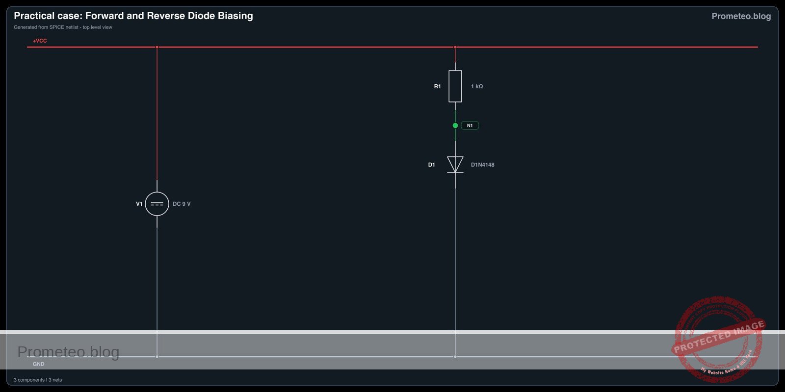
* Voltage Drop: Measurement of the characteristic forward voltage drop (~0.6 V to 0.7 V) across the silicon diode.
Target audience: Hobbyists and basic electronics students.
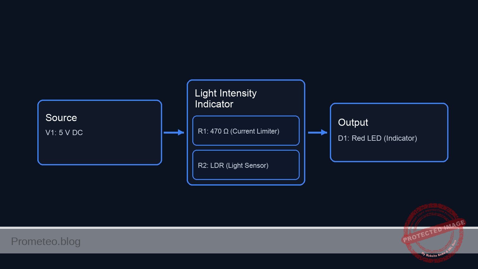
Materials
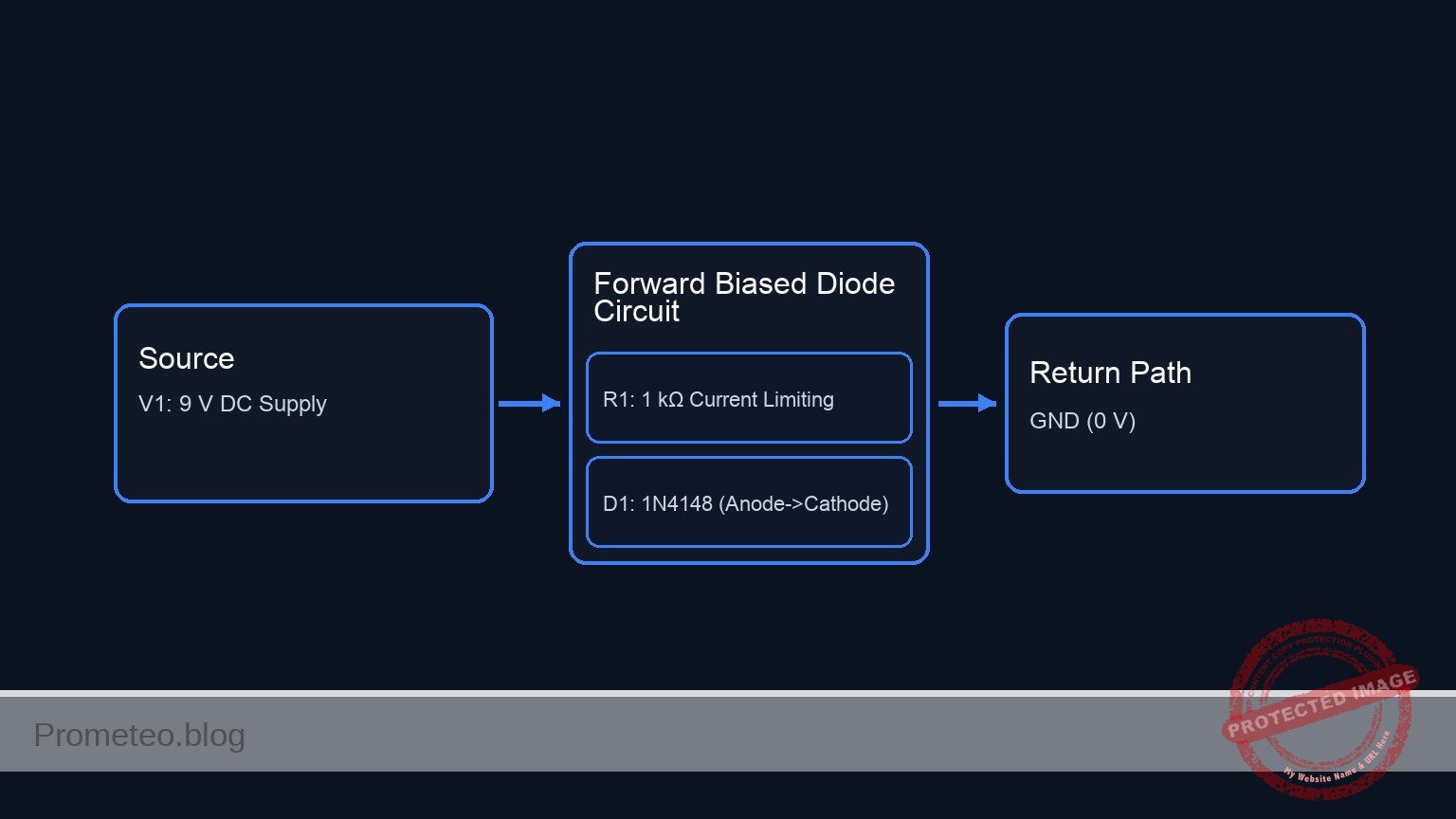
- V1: 9 V Battery or DC Power Supply, function: Main energy source.
- D1: 1N4007 Rectifier Diode, function: Blocks current flow in reverse direction.
- M1: 9 V DC Hobby Motor, function: The sensitive load being protected.
- S1: SPST Toggle Switch (Optional), function: Master ON/OFF control.
Wiring guide
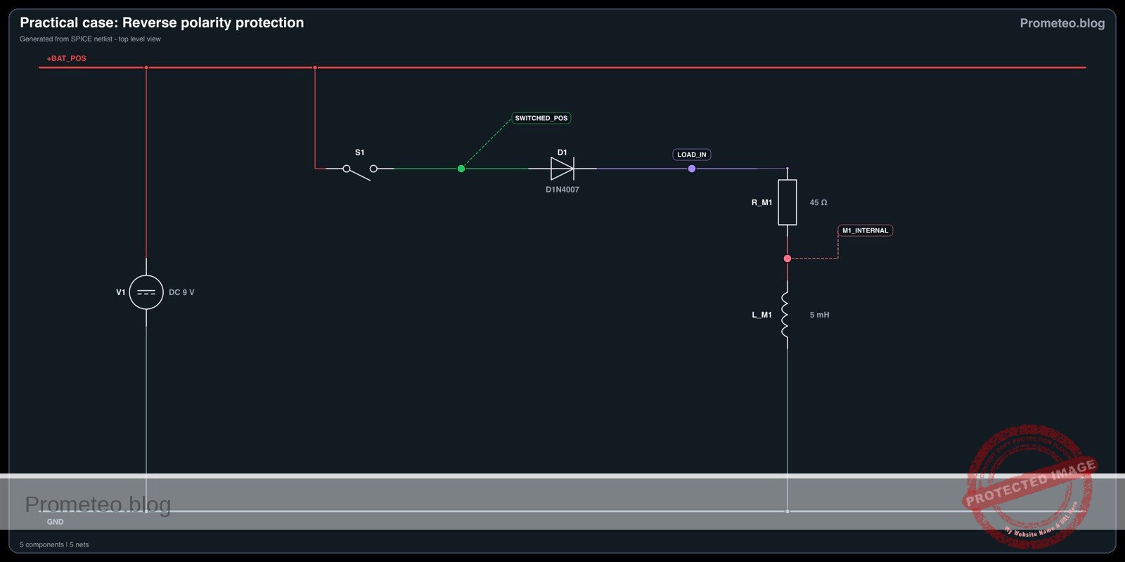
This circuit puts the diode in series with the positive rail of the power supply.
- V1 (Positive Terminal) connects to node
BAT_POS. - V1 (Negative Terminal) connects to node
0(GND). - S1 (if used) connects between
BAT_POSand nodeSWITCHED_POS. (If not used, connectBAT_POSdirectly toSWITCHED_POS). - D1 (Anode) connects to node
SWITCHED_POS. - D1 (Cathode) connects to node
LOAD_IN. (The striped band on the physical component marks the cathode). - M1 (Positive Terminal) connects to node
LOAD_IN. - M1 (Negative Terminal) connects to node
0(GND).
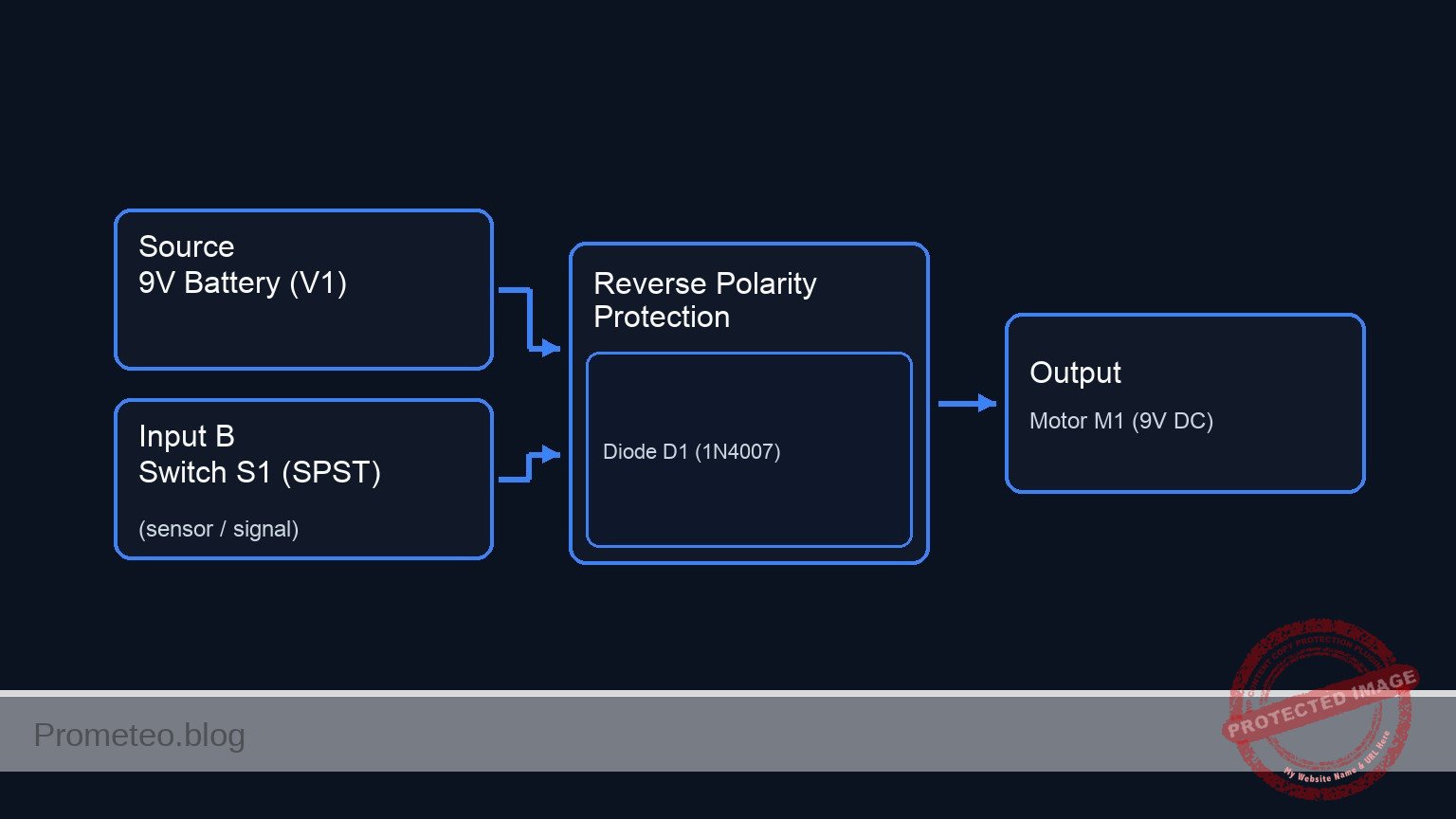
Conceptual block diagram
Schematic
[ POWER SOURCE ]              [ LOGIC / PROTECTION ]                 [ OUTPUT LOAD ]

+---------------------+       +-----------+        +--------------+       +--------------+
|   9 V Battery (V1)   |       | Switch S1 |        |   Diode D1   |       |   Motor M1   |
|      (Positive)     |------>|  (SPST)   |------->|   (1N4007)   |------>|   (9 V DC)    |-----> [ GND ]
+---------------------+   ^   +-----------+    ^   | Anode->Cath  |   ^   +--------------+
                          |                    |   +--------------+   |
                      (BAT_POS)          (SWITCHED_POS)           (LOAD_IN)
Electrical diagram
Measurements and tests
To validate the protection, perform the following steps using a multimeter:
-
Forward Bias Test (Normal Operation):
- Connect V1 correctly (Positive to Anode side).
- Observe: The motor M1 spins.
- Measure: Place the red probe on
LOAD_INand the black probe on0(GND). Expect a reading of approx. 8.3 V to 8.4 V (9 V input minus the diode drop).
-
Diode Drop Measurement:
- With the circuit powered ON, place probes across D1 (Red on
SWITCHED_POS, Black onLOAD_IN). - Result: You should read approximately 0.6 V to 0.7 V. This confirms the diode is conducting.
- With the circuit powered ON, place probes across D1 (Red on
-
Reverse Bias Test (Simulation of Error):
- Disconnect V1 and reverse the connections (Positive to GND, Negative to the input of the switch/diode).
- Observe: The motor M1 does not spin. It is completely safe.
- Measure: Place the red probe on
LOAD_INand the black probe on the battery negative (now at the top). The reading should be 0 V. Current is blocked.
SPICE netlist and simulation
Reference SPICE Netlist (ngspice) — excerptFull SPICE netlist (ngspice)
* TITLE: Practical case: Reverse polarity protection

* --- Bill of Materials & Component Models ---

* V1: 9 V Battery or DC Power Supply
* Function: Main energy source
* Connected between BAT_POS and GND (0)
V1 BAT_POS 0 DC 9

* S1: SPST Toggle Switch
* Function: Master ON/OFF control
* Connected between BAT_POS and SWITCHED_POS
* Modeled as a voltage-controlled switch driven by a stimulus source to simulate user action.
S1 BAT_POS SWITCHED_POS CTRL_NODE 0 SW_MODEL
.model SW_MODEL SW(Vt=2.5 Ron=0.1 Roff=100Meg)

* Stimulus for S1 (User pressing the switch)
* Switch is OPEN (0V) initially, closes (5V) at 100us.
V_S1_ACT CTRL_NODE 0 PULSE(0 5 100u 1u 1u 10m 20m)

* ... (truncated in public view) ...
Copy this content into a .cir file and run with ngspice.
* TITLE: Practical case: Reverse polarity protection

* --- Bill of Materials & Component Models ---

* V1: 9 V Battery or DC Power Supply
* Function: Main energy source
* Connected between BAT_POS and GND (0)
V1 BAT_POS 0 DC 9

* S1: SPST Toggle Switch
* Function: Master ON/OFF control
* Connected between BAT_POS and SWITCHED_POS
* Modeled as a voltage-controlled switch driven by a stimulus source to simulate user action.
S1 BAT_POS SWITCHED_POS CTRL_NODE 0 SW_MODEL
.model SW_MODEL SW(Vt=2.5 Ron=0.1 Roff=100Meg)

* Stimulus for S1 (User pressing the switch)
* Switch is OPEN (0V) initially, closes (5V) at 100us.
V_S1_ACT CTRL_NODE 0 PULSE(0 5 100u 1u 1u 10m 20m)

* D1: 1N4007 Rectifier Diode
* Function: Blocks current flow in reverse direction
* Anode -> SWITCHED_POS, Cathode -> LOAD_IN
D1 SWITCHED_POS LOAD_IN D1N4007
* Standard generic model for 1N4007
.model D1N4007 D(IS=7.03n RS=0.034 N=1.8 BV=1000 IBV=5u CJO=10p VJ=0.7 M=0.5 TT=100n)

* M1: 9 V DC Hobby Motor
* Function: The sensitive load being protected
* Connected between LOAD_IN and GND (0)
* Modeled as a Series Resistor (winding resistance) and Inductor
R_M1 LOAD_IN M1_INTERNAL 45
L_M1 M1_INTERNAL 0 5m

* --- Analysis & Output Directives ---

* Transient analysis to observe the switch turning on and voltage drop across diode
.tran 10u 2m

* Print directives for ngspice batch mode
.print tran V(BAT_POS) V(SWITCHED_POS) V(LOAD_IN)

* Operating point analysis
.op

.end
Simulation Results (Transient Analysis)

Show raw data table (233 rows)
Index   time            v(bat_pos)      v(switched_pos) v(load_in)
0	0.000000e+00	9.000000e+00	1.216207e-01	3.995271e-06
1	1.000000e-07	9.000000e+00	1.216207e-01	3.995280e-06
2	2.000000e-07	9.000000e+00	1.216207e-01	3.995265e-06
3	4.000000e-07	9.000000e+00	1.216207e-01	3.995282e-06
4	8.000000e-07	9.000000e+00	1.216207e-01	3.995257e-06
5	1.600000e-06	9.000000e+00	1.216207e-01	3.995290e-06
6	3.200000e-06	9.000000e+00	1.216207e-01	3.995250e-06
7	6.400000e-06	9.000000e+00	1.216207e-01	3.995292e-06
8	1.280000e-05	9.000000e+00	1.216207e-01	3.995249e-06
9	2.280000e-05	9.000000e+00	1.216207e-01	3.995292e-06
10	3.280000e-05	9.000000e+00	1.216207e-01	3.995249e-06
11	4.280000e-05	9.000000e+00	1.216207e-01	3.995292e-06
12	5.280000e-05	9.000000e+00	1.216207e-01	3.995249e-06
13	6.280000e-05	9.000000e+00	1.216207e-01	3.995292e-06
14	7.280000e-05	9.000000e+00	1.216207e-01	3.995249e-06
15	8.280000e-05	9.000000e+00	1.216207e-01	3.995292e-06
16	9.280000e-05	9.000000e+00	1.216207e-01	3.995249e-06
17	1.000000e-04	9.000000e+00	1.216207e-01	3.995292e-06
18	1.001000e-04	9.000000e+00	1.216207e-01	3.995267e-06
19	1.002600e-04	9.000000e+00	1.216207e-01	3.995284e-06
20	1.003075e-04	9.000000e+00	1.216207e-01	3.995227e-06
21	1.003906e-04	9.000000e+00	1.216207e-01	3.995299e-06
22	1.004136e-04	9.000000e+00	1.216207e-01	3.995334e-06
23	1.004539e-04	9.000000e+00	1.216207e-01	3.995198e-06
... (209 more rows) ...
Common mistakes and how to avoid them
- Installing the diode backwards: The circuit will not work even with the correct battery polarity. Always ensure the silver band (cathode) points toward the load (M1).
- Using a signal diode for high loads: Using a small 1N4148 for a high-current motor may cause the diode to overheat and fail. Use a 1N400x series diode (1 A rating) for motors.
- Ignoring voltage drop: Students often forget that the diode «eats» about 0.7 V. If your load requires exactly 9 V, supplying 9 V through a diode might result in under-performance (8.3 V).
Troubleshooting
- Symptom: Motor runs slower than expected.
- Cause: The voltage drop across the diode reduces the effective voltage at the motor.
- Fix: Increase the supply voltage slightly or use a Schottky diode.
- Symptom: Diode gets very hot.
- Cause: The motor draws more current than the diode is rated for.
- Fix: Check the motor’s current draw and replace D1 with a higher amperage diode (e.g., 1N5408 for 3 A).
- Symptom: Motor works in both battery orientations.
- Cause: The diode has failed short (internal damage) or is bypassed by a wire.
- Fix: Test the diode with the «Diode Check» function on a multimeter; replace if it conducts in both directions.
Possible improvements and extensions
- Schottky Diode Upgrade: Replace the 1N4007 with a 1N5817 (Schottky). Measure the voltage drop again; it should be lower (~0.3 V), making the circuit more efficient.
- Full Bridge Rectifier: Replace the single diode with a bridge rectifier consisting of 4 diodes. This allows the device to work regardless of polarity (auto-correction) rather than just blocking the wrong polarity.
More Practical Cases on Prometeo.blog
        <div class="amazon-affiliate">
          <p><strong>Find this product and/or books on this topic on Amazon</strong></p>
          <p><a class="amazon-affiliate-btn" href="https://amzn.to/4mt8r4C" target="_blank" rel="nofollow sponsored noopener">Go to Amazon</a></p>
          <p class="amazon-affiliate-disclaimer">As an Amazon Associate, I earn from qualifying purchases. If you buy through this link, you help keep this project running.</p>
        </div>
Quick Quiz

Telecommunications Electronics Engineer and Computer Engineer (official degrees in Spain).