Practical case: Simple twilight switch

Simple twilight switch prototype (Maker Style)

Level: Basic. Objective: Build a circuit that activates an LED when light levels drop.

Objective and use case

In this practical case, you will design and assemble a light-sensing circuit that automatically turns on an LED when the environment becomes dark. This circuit uses a photodiode to control an NPN transistor acting as a switch.

  • Real-world applications:
    • Automatic street lighting systems.
    • Emergency corridor lights that activate during power outages (if light absent).
    • Battery-saving garden solar lights.
    • Security systems triggered by shadows or obstruction of light beams.
  • Expected outcome:
    • Bright light: The LED remains OFF; the voltage at the transistor base is low.
    • Darkness: The LED turns ON; the voltage at the transistor base rises above 0.7 V.
    • Transition: The circuit reacts to the absence of light (dark sensor logic).
  • Target audience: Beginners and electronics students.

Materials

  • V1: 5 V DC supply, function: main power source.
  • R1: 100 kΩ resistor, function: base pull-up resistor (sets sensitivity).
  • R2: 330 Ω resistor, function: LED current limiting.
  • D1: Generic silicon photodiode, function: light sensor.
  • Q1: 2N2222 (or BC547) NPN Transistor, function: electronic switch.
  • D2: Red LED, function: visual output indicator.

Wiring guide

This guide uses specific node names to define the connections clearly.
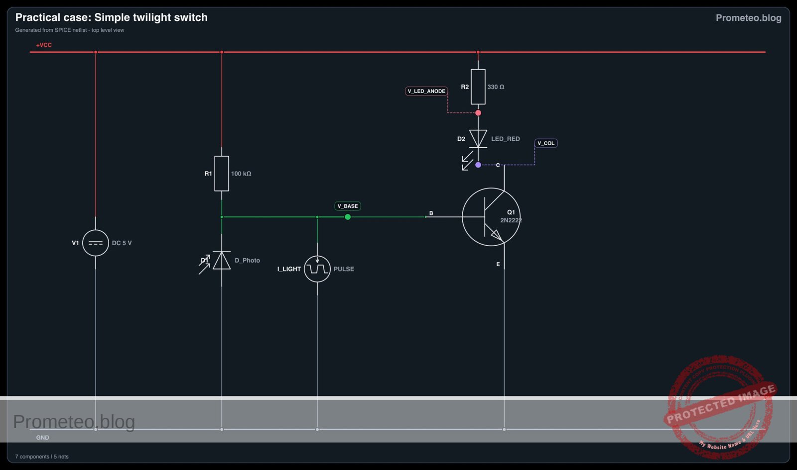
* Nodes defined: VCC (5 V), GND (0 V), V_BASE (Control voltage), V_COL (Collector voltage).

  • V1 (Source): Connect positive terminal to VCC and negative terminal to GND.
  • R1 (Bias): Connect between VCC and V_BASE.
  • D1 (Photodiode):
    • Connect the Cathode to V_BASE.
    • Connect the Anode to GND.
    • Note: The photodiode is used in reverse bias mode.
  • Q1 (Transistor):
    • Connect the Base to V_BASE.
    • Connect the Emitter to GND.
    • Connect the Collector to V_COL.
  • R2 & D2 (Output Loop):
    • Connect R2 between VCC and the Anode of D2.
    • Connect the Cathode of D2 to V_COL (the Collector of Q1).

Conceptual block diagram

Conceptual block diagram — 74HC14 Photodiode
Quick read: inputs → main block → output (actuator or measurement). This summarizes the ASCII schematic below.

Schematic

[ INPUT / SENSING ]                     [ LOGIC / SWITCHING ]                   [ OUTPUT / LOAD ]

      [ VCC (5 V) ]                                                                       [ VCC (5 V) ]
           |                                                                                  |
           |                                                                                  |
           v                                                                                  v
    [ R1: 100k Bias ] --(Pull Up)--+                                                  [ R2: 330 Ohm ]
                                   |                                                          |
                                   |                                                          |
                                (V_BASE)                                                      v
                                   |                                                    [ D2: Red LED ]
                                   |                                                          |
                                   +--(Control Sig)--> [ Q1: NPN Base ]                       |
                                   |                   [              ]                       |
                                   |                   [ Q1 Collector ] <--(Sink Current)-----+
    [ D1: Photodiode ] --(Sensor)--+                   [              ]                 (V_COL Node)
    (Reverse Biased)               |                   [ Q1 Emitter   ]
           |                       |                          |
           |                       |                          |
           v                       |                          v
        [ GND ]                    +---------------------> [ GND ]
Schematic (ASCII)

Electrical diagram

Electrical diagram for case: Practical case: Simple twilight switch
Generated from the validated SPICE netlist for this case.

🔒 This electrical diagram is premium. With the monthly membership (7-day free trial) you can unlock the complete didactic material and the print-ready PDF pack.🔓 See premium access plans

Measurements and tests

Perform the following validation steps using a multimeter to ensure the circuit works as intended.

  1. Check Supply Voltage:
    • Measure between VCC and GND. It should read approximately 5 V.
  2. Test Light Condition (LED OFF):
    • Shine a bright light directly on the photodiode D1.
    • Measure voltage at V_BASE. It should be low (typically < 0.5 V) because the photodiode conducts current to ground.
    • Observe D2 (LED). It should be OFF.
    • Measure voltage at V_COL. It should be close to VCC (High) as the transistor is in cutoff.
  3. Test Dark Condition (LED ON):
    • Cover D1 completely with your hand or a dark cap.
    • Measure voltage at V_BASE. It should rise above 0.6 V – 0.7 V.
    • Observe D2 (LED). It should turn ON.
    • Measure voltage at V_COL. It should drop to near 0 V (saturation voltage ~0.2 V).

SPICE netlist and simulation

Reference SPICE Netlist (ngspice) — excerptFull SPICE netlist (ngspice)

* Practical case: Simple twilight switch

* --- Power Supply ---
* V1: 5 V DC supply
V1 VCC 0 DC 5

* --- Input Stage (Light Sensor) ---
* R1: 100 kΩ resistor (Base pull-up)
* Connect between VCC and V_BASE
R1 VCC V_BASE 100k

* D1: Generic silicon photodiode
* Connect the Cathode to V_BASE, Anode to GND (Reverse Bias)
* SPICE Syntax: Dname Anode Cathode Model
D1 0 V_BASE D_GENERIC

* OPTICAL STIMULUS SIMULATION
* The photodiode generates a photocurrent flowing from Cathode to Anode 
* (Reverse current) proportional to light intensity.
* We simulate this with a Current Source (I_LIGHT) in parallel with D1.
* ... (truncated in public view) ...

Copy this content into a .cir file and run with ngspice.

🔒 Part of this section is premium. With the monthly membership (7-day free trial) you can access the full content (materials, wiring, detailed build, validation, troubleshooting, variants and checklist) and download the complete print-ready PDF pack.

* Practical case: Simple twilight switch

* --- Power Supply ---
* V1: 5 V DC supply
V1 VCC 0 DC 5

* --- Input Stage (Light Sensor) ---
* R1: 100 kΩ resistor (Base pull-up)
* Connect between VCC and V_BASE
R1 VCC V_BASE 100k

* D1: Generic silicon photodiode
* Connect the Cathode to V_BASE, Anode to GND (Reverse Bias)
* SPICE Syntax: Dname Anode Cathode Model
D1 0 V_BASE D_GENERIC

* OPTICAL STIMULUS SIMULATION
* The photodiode generates a photocurrent flowing from Cathode to Anode 
* (Reverse current) proportional to light intensity.
* We simulate this with a Current Source (I_LIGHT) in parallel with D1.
* Logic: 
*   0uA = Dark (Night) -> Base High -> Q1 ON -> LED ON
*   100uA = Light (Day) -> Base Low -> Q1 OFF -> LED OFF
* Waveform: Dark (0uA) transitioning to Light (100uA)
I_LIGHT V_BASE 0 PULSE(0 100u 100u 100u 100u 2m 5m)

* --- Switching Stage ---
* Q1: 2N2222 NPN Transistor
* Base to V_BASE, Emitter to GND, Collector to V_COL
* SPICE Syntax: Qname Collector Base Emitter Model
Q1 V_COL V_BASE 0 2N2222

* --- Output Stage ---
* R2: 330 Ω resistor
* Connect between VCC and the Anode of D2 (Node V_LED_ANODE)
R2 VCC V_LED_ANODE 330

* D2: Red LED
* Connect Anode to V_LED_ANODE, Cathode to V_COL
D2 V_LED_ANODE V_COL LED_RED

* --- Models ---
* Standard NPN Transistor Model
.model 2N2222 NPN (IS=1E-14 VAF=100 BF=200 IKF=0.3 XTB=1.5 BR=3 CJC=8E-12 CJE=25E-12 TR=46.91E-9 TF=411.1E-12 ITF=0.6 VTF=1.7 XTF=3 RB=10 RC=1 RE=0.1)

* Generic Red LED Model (Approx 1.8V-2V drop)
.model LED_RED D (IS=93.2p RS=42m N=3.73 BV=5 IBV=10u CJO=2.97p VJ=0.75 M=0.333 TT=4.32u)

* Generic Silicon Diode Model for Photodiode (Dark characteristics)
.model D_GENERIC D (IS=1N N=1 RS=0.1)

* --- Analysis Directives ---
* Transient analysis to show the switching behavior
.tran 10u 5m

* Print required voltages to verify operation
* V(V_BASE): Sensor voltage (High = Dark, Low = Light)
* V(V_COL): Output state (Low = LED ON, High/Floating = LED OFF)
.print tran V(V_BASE) V(V_COL)

.op
.end

Simulation Results (Transient Analysis)

Simulation Results (Transient Analysis)
Show raw data table (534 rows)
Index   time            v(v_base)       v(v_col)
0	0.000000e+00	7.119659e-01	4.863696e-01
1	1.000000e-07	7.119659e-01	4.863696e-01
2	2.000000e-07	7.119659e-01	4.863696e-01
3	4.000000e-07	7.119659e-01	4.863696e-01
4	8.000000e-07	7.119659e-01	4.863696e-01
5	1.600000e-06	7.119659e-01	4.863696e-01
6	3.200000e-06	7.119659e-01	4.863696e-01
7	6.400000e-06	7.119659e-01	4.863696e-01
8	1.280000e-05	7.119659e-01	4.863696e-01
9	2.280000e-05	7.119659e-01	4.863696e-01
10	3.280000e-05	7.119659e-01	4.863696e-01
11	4.280000e-05	7.119659e-01	4.863696e-01
12	5.280000e-05	7.119659e-01	4.863696e-01
13	6.280000e-05	7.119659e-01	4.863696e-01
14	7.280000e-05	7.119659e-01	4.863696e-01
15	8.280000e-05	7.119659e-01	4.863696e-01
16	9.280000e-05	7.119659e-01	4.863696e-01
17	1.000000e-04	7.119659e-01	4.863696e-01
18	1.006859e-04	7.117420e-01	5.075675e-01
19	1.020576e-04	7.110644e-01	5.716214e-01
20	1.044620e-04	7.094358e-01	7.222583e-01
21	1.068767e-04	7.077111e-01	8.743413e-01
22	1.096009e-04	7.056321e-01	1.048175e+00
23	1.150494e-04	7.009675e-01	1.400214e+00
... (510 more rows) ...


Reference SPICE netlist (ngspice)

* Practical case: Simple twilight switch

* --- Power Supply ---
* V1: 5 V DC supply
V1 VCC 0 DC 5

* --- Input Stage (Light Sensor) ---
* R1: 100 kΩ resistor (Base pull-up)
* Connect between VCC and V_BASE
R1 VCC V_BASE 100k

* D1: Generic silicon photodiode
* Connect the Cathode to V_BASE, Anode to GND (Reverse Bias)
* SPICE Syntax: Dname Anode Cathode Model
D1 0 V_BASE D_GENERIC

* OPTICAL STIMULUS SIMULATION
* The photodiode generates a photocurrent flowing from Cathode to Anode
* (Reverse current) proportional to light intensity.
* We simulate this with a Current Source (I_LIGHT) in parallel with D1.
* Logic:
*   0uA = Dark (Night) -> Base High -> Q1 ON -> LED ON
*   100uA = Light (Day) -> Base Low -> Q1 OFF -> LED OFF
* Waveform: Dark (0uA) transitioning to Light (100uA)
I_LIGHT V_BASE 0 PULSE(0 100u 100u 100u 100u 2m 5m)

* --- Switching Stage ---
* Q1: 2N2222 NPN Transistor
* Base to V_BASE, Emitter to GND, Collector to V_COL
* SPICE Syntax: Qname Collector Base Emitter Model
Q1 V_COL V_BASE 0 2N2222

* --- Output Stage ---
* R2: 330 Ω resistor
* Connect between VCC and the Anode of D2 (Node V_LED_ANODE)
R2 VCC V_LED_ANODE 330

* D2: Red LED
* Connect Anode to V_LED_ANODE, Cathode to V_COL
D2 V_LED_ANODE V_COL LED_RED

* --- Models ---
* Standard NPN Transistor Model
.model 2N2222 NPN (IS=1E-14 VAF=100 BF=200 IKF=0.3 XTB=1.5 BR=3 CJC=8E-12 CJE=25E-12 TR=46.91E-9 TF=411.1E-12 ITF=0.6 VTF=1.7 XTF=3 RB=10 RC=1 RE=0.1)

* Generic Red LED Model (Approx 1.8V-2V drop)
.model LED_RED D (IS=93.2p RS=42m N=3.73 BV=5 IBV=10u CJO=2.97p VJ=0.75 M=0.333 TT=4.32u)

* Generic Silicon Diode Model for Photodiode (Dark characteristics)
.model D_GENERIC D (IS=1N N=1 RS=0.1)

* --- Analysis Directives ---
* Transient analysis to show the switching behavior
.tran 10u 5m

* Print required voltages to verify operation
* V(V_BASE): Sensor voltage (High = Dark, Low = Light)
* V(V_COL): Output state (Low = LED ON, High/Floating = LED OFF)
.print tran V(V_BASE) V(V_COL)

.op
.end

Simulation Results (Transient Analysis)

Simulation Results (Transient Analysis)

Common mistakes and how to avoid them

  1. Reversing the Photodiode:
    • Error: Connecting the Anode to Base and Cathode to Ground.
    • Result: The diode acts like a standard forward-biased diode, clamping the Base to ~0.7 V permanently or conducting fully, preventing the switching logic.
    • Solution: Ensure the Cathode (marked with a line or flat side) connects to the positive side (Base) for reverse bias operation.
  2. Incorrect Transistor Pinout:
    • Error: Swapping Collector and Emitter on the 2N2222.
    • Result: The gain is significantly reduced, and the LED may not turn on fully or the transistor might overheat.
    • Solution: Verify the pinout (E-B-C) in the datasheet before insertion.
  3. Wrong Resistor Value for R1:
    • Error: Using a very low value (e.g., 1 kΩ) for R1.
    • Result: The photodiode current cannot pull the voltage down enough in bright light, keeping the LED ON permanently.
    • Solution: Use a high value (100 kΩ to 330 kΩ) to allow the small photocurrent to control the voltage divider effectively.

Troubleshooting

  • Symptom: LED is always ON, even in bright light.
    • Cause: R1 is too small, or the ambient light is not strong enough to generate sufficient photocurrent.
    • Fix: Increase R1 to 220 kΩ or 330 kΩ, or bring the light source closer.
  • Symptom: LED is always OFF, even in total darkness.
    • Cause: Photodiode is shorted, R1 is open, or Transistor is blown.
    • Fix: Check continuity on R1. Remove D1; if LED turns on, D1 was shorted or installed backward (forward biased).
  • Symptom: LED glows dimly in the dark.
    • Cause: Q1 is not fully saturating.
    • Fix: Decrease R2 slightly (ensure it stays above 220 Ω) or check if V1 is actually 5 V.

Possible improvements and extensions

  1. Sensitivity Adjustment: Replace R1 with a 500 kΩ potentiometer (in series with a 10 kΩ safety resistor) to manually tune the light level at which the LED triggers.
  2. Hysteresis/Clean Switching: Add a second transistor or a Schmitt Trigger (e.g., 74HC14) between the photodiode node and the driver transistor to prevent the LED from flickering at the «twilight» threshold.

More Practical Cases on Prometeo.blog

Find this product and/or books on this topic on Amazon

Go to Amazon

As an Amazon Associate, I earn from qualifying purchases. If you buy through this link, you help keep this project running.

Quick Quiz

Question 1: What is the primary objective of the circuit described in the text?


Question 2: Which component acts as the electronic switch in this circuit?


Question 3: What happens to the LED when the environment is bright?


Question 4: What is the function of the 330 Ω resistor (R2)?


Question 5: Which voltage threshold at the transistor base is mentioned for turning the LED ON?


Question 6: What real-world application is listed for this type of circuit?


Question 7: What is the role of resistor R1 (100 kΩ)?


Question 8: What is the function of the V1 component in the materials list?


Question 9: How does the circuit behave during the transition from light to dark?


Question 10: Who is the target audience for this circuit project?


Carlos Núñez Zorrilla
Electronics & Computer Engineer

Telecommunications Electronics Engineer and Computer Engineer (official degrees in Spain).
Follow me:


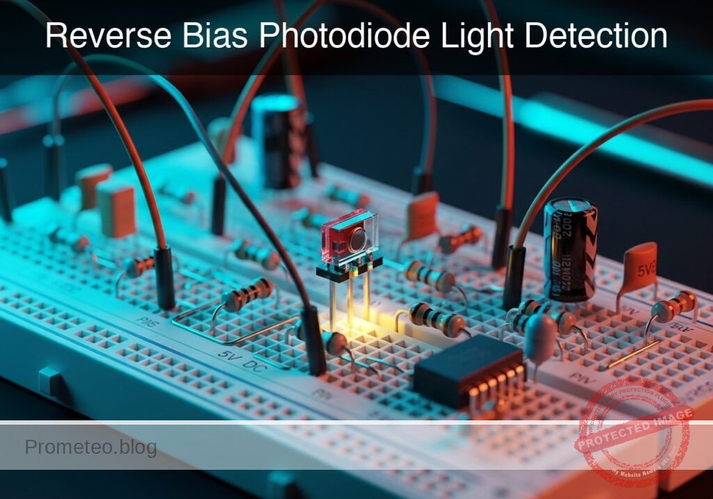
Practical case: Reverse Bias Photodiode Light Detection

Reverse Bias Photodiode Light Detection prototype (Maker Style)

Level: Basic – Understand how a reverse-biased photodiode acts as a light sensor.

Objective and use case

In this practical case, you will build a circuit that utilizes a photodiode in reverse bias mode to detect varying levels of light intensity. By measuring the voltage drop across a series resistor, you will observe the relationship between photon incidence and leakage current.

  • Real-world utility:

    • Optical communications: Used in fiber optic receivers to convert light pulses back into electrical data.
    • Smoke detectors: Detects light scattered by smoke particles in an optical chamber.
    • Ambient light sensors: Adjusts screen brightness on smartphones based on surrounding light.
    • Safety curtains: Stops industrial machinery when a light beam is interrupted.
  • Expected outcome:

    • Dark condition: The voltage output will be near 0 V (minimal dark current).
    • Light condition: The voltage output will rise proportionally to the light intensity.
    • Linearity: The photodiode acts as a current source where Iphoto is linear with respect to illuminance (Lux).
  • Target audience: Students and hobbyists introducing themselves to semiconductor sensors.

Materials

  • V1: 5 V DC supply, function: Reverse bias voltage source.
  • D1: Photodiode (e.g., BPW34 or generic silicon photodiode), function: Light sensor.
  • R1: 100 kΩ resistor, function: Current-to-voltage conversion (Load resistor).
  • L1: White LED or Flashlight, function: External light stimulus.
  • M1: Multimeter, function: Voltmeter for V_OUT.

Wiring guide

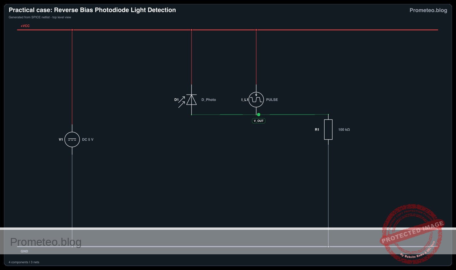
This circuit uses a series configuration to measure the reverse photocurrent. We define the nodes as VCC (5 V source), V_OUT (Measurement point), and 0 (Ground).

  • V1: Connect the positive terminal to node VCC and the negative terminal to node 0.
  • D1 (Photodiode): Connect the Cathode (marked side) to node VCC. Connect the Anode to node V_OUT. Note: This ensures the diode is reverse-biased.
  • R1: Connect one leg to node V_OUT and the other leg to node 0.
  • M1 (Voltmeter): Connect the positive probe to V_OUT and the negative probe to 0.

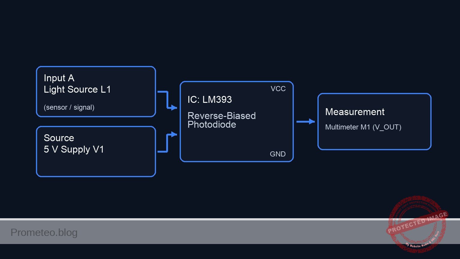
Conceptual block diagram

Conceptual block diagram — LM393 Reverse-Biased Photodiode
Quick read: inputs → main block → output (actuator or measurement). This summarizes the ASCII schematic below.

Schematic

[ STIMULUS & POWER ]               [ SENSOR LOGIC ]                     [ OUTPUT ]

    [ Light Source L1 ] ~~~(Light)~~~>+---------------------+
                                      |    Photodiode D1    |
                                      | (Sensor / Rev Bias) |
    [ 5 V Supply V1 ] -----(VCC)------>| Cathode       Anode |----(V_OUT)---> [ Multimeter M1 ]
                                      +----------+----------+      (Volts)
                                                 |
                                           (Photocurrent)
                                                 |
                                                 v
                                      +----------+----------+
                                      |     Resistor R1     |
                                      |      (100 kΩ)       |
                                      +----------+----------+
                                                 |
                                                 v
                                          [ GND (0 V) ]
Schematic (ASCII)

Electrical diagram

Electrical diagram for case: Reverse Bias Photodiode Light Detection
Generated from the validated SPICE netlist for this case.

🔒 This electrical diagram is premium. With the monthly membership (7-day free trial) you can unlock the complete didactic material and the print-ready PDF pack.🔓 See premium access plans

Measurements and tests

  1. Dark Test: Cover the photodiode completely with an opaque object or your hand. Measure the voltage at V_OUT.
    • Expectation: The reading should be very close to 0 V (typically in the microvolt or low millivolt range), representing the dark current.
  2. Ambient Light Test: Expose the sensor to normal room lighting.
    • Expectation: V_OUT should rise significantly (e.g., 0.5 V to 2.0 V, depending on brightness and the exact value of R1).
  3. High Intensity Test: Shine a flashlight or bright LED (L1) directly at D1.
    • Expectation: V_OUT should increase further, potentially approaching the supply voltage limit if the light is very intense.
  4. Calculation: Use Ohm’s Law to calculate the photocurrent at any specific light level: Ireverse = VOUT / R1.

SPICE netlist and simulation

Reference SPICE Netlist (ngspice) — excerptFull SPICE netlist (ngspice)

* Practical case: Reverse Bias Photodiode Light Detection

* --- Models ---
* Generic Photodiode Model (Approximation for BPW34)
* Parameters: IS (Sat Current), CJO (Junction Cap), BV (Breakdown), RS (Series Res)
.model BPW34 D(IS=10n RS=5 N=1.1 BV=60 IBV=10u CJO=70p M=0.45 VJ=0.75)

* --- Components ---

* V1: 5 V DC supply
* Wiring: Positive to VCC, Negative to 0 (Ground)
V1 VCC 0 DC 5

* D1: Photodiode (Sensor)
* Wiring Guide: Cathode to VCC, Anode to V_OUT
* Note: SPICE Diode syntax is D   
D1 V_OUT VCC BPW34

* L1: External Light Stimulus (White LED/Flashlight)
* Modeled as a Current Source (I_L1) representing the generated photocurrent.
* ... (truncated in public view) ...

Copy this content into a .cir file and run with ngspice.

🔒 Part of this section is premium. With the monthly membership (7-day free trial) you can access the full content (materials, wiring, detailed build, validation, troubleshooting, variants and checklist) and download the complete print-ready PDF pack.

* Practical case: Reverse Bias Photodiode Light Detection

* --- Models ---
* Generic Photodiode Model (Approximation for BPW34)
* Parameters: IS (Sat Current), CJO (Junction Cap), BV (Breakdown), RS (Series Res)
.model BPW34 D(IS=10n RS=5 N=1.1 BV=60 IBV=10u CJO=70p M=0.45 VJ=0.75)

* --- Components ---

* V1: 5 V DC supply
* Wiring: Positive to VCC, Negative to 0 (Ground)
V1 VCC 0 DC 5

* D1: Photodiode (Sensor)
* Wiring Guide: Cathode to VCC, Anode to V_OUT
* Note: SPICE Diode syntax is D   
D1 V_OUT VCC BPW34

* L1: External Light Stimulus (White LED/Flashlight)
* Modeled as a Current Source (I_L1) representing the generated photocurrent.
* In reverse bias, photocurrent flows from Cathode to Anode (internally),
* effectively injecting current from VCC into V_OUT.
* Simulation: Pulsing light from Dark (0A) to Light (30uA).
* Timing: Delay 100us, Rise/Fall 10us, Width 400us, Period 1ms.
I_L1 VCC V_OUT PULSE(0 30u 100u 10u 10u 400u 1m)

* R1: 100 kOhm Load Resistor
* Wiring: One leg to V_OUT, other leg to 0
R1 V_OUT 0 100k

* M1: Multimeter (Voltmeter)
* Function: Measure voltage at V_OUT relative to Ground.
* Implemented via .print output directives below.

* --- Analysis Directives ---

* Transient Analysis:
* Step: 10us, Stop: 3ms (Captures 3 full light pulses)
.tran 10u 3m

* Operating Point Analysis (Initial DC Check):
.op

* Output Printing:
* Prints the voltage at the output node (V_OUT) and supply (VCC)
.print tran V(V_OUT) V(VCC)

.end

Simulation Results (Transient Analysis)

Simulation Results (Transient Analysis)
Show raw data table (347 rows)
Index   time            v(v_out)        v(vcc)
0	0.000000e+00	1.000500e-03	5.000000e+00
1	1.000000e-07	1.000500e-03	5.000000e+00
2	2.000000e-07	1.000500e-03	5.000000e+00
3	4.000000e-07	1.000500e-03	5.000000e+00
4	8.000000e-07	1.000500e-03	5.000000e+00
5	1.600000e-06	1.000500e-03	5.000000e+00
6	3.200000e-06	1.000500e-03	5.000000e+00
7	6.400000e-06	1.000500e-03	5.000000e+00
8	1.280000e-05	1.000500e-03	5.000000e+00
9	2.280000e-05	1.000500e-03	5.000000e+00
10	3.280000e-05	1.000500e-03	5.000000e+00
11	4.280000e-05	1.000500e-03	5.000000e+00
12	5.280000e-05	1.000500e-03	5.000000e+00
13	6.280000e-05	1.000500e-03	5.000000e+00
14	7.280000e-05	1.000500e-03	5.000000e+00
15	8.280000e-05	1.000500e-03	5.000000e+00
16	9.280000e-05	1.000500e-03	5.000000e+00
17	1.000000e-04	1.000500e-03	5.000000e+00
18	1.010000e-04	7.978912e-02	5.000000e+00
19	1.030000e-04	3.507154e-01	5.000000e+00
20	1.070000e-04	1.270928e+00	5.000000e+00
21	1.100000e-04	2.076364e+00	5.000000e+00
22	1.108000e-04	2.250021e+00	5.000000e+00
23	1.124000e-04	2.525718e+00	5.000000e+00
... (323 more rows) ...


Reference SPICE netlist (ngspice)

* Practical case: Reverse Bias Photodiode Light Detection

* --- Models ---
* Generic Photodiode Model (Approximation for BPW34)
* Parameters: IS (Sat Current), CJO (Junction Cap), BV (Breakdown), RS (Series Res)
.model BPW34 D(IS=10n RS=5 N=1.1 BV=60 IBV=10u CJO=70p M=0.45 VJ=0.75)

* --- Components ---

* V1: 5 V DC supply
* Wiring: Positive to VCC, Negative to 0 (Ground)
V1 VCC 0 DC 5

* D1: Photodiode (Sensor)
* Wiring Guide: Cathode to VCC, Anode to V_OUT
* Note: SPICE Diode syntax is D
D1 V_OUT VCC BPW34

* L1: External Light Stimulus (White LED/Flashlight)
* Modeled as a Current Source (I_L1) representing the generated photocurrent.
* In reverse bias, photocurrent flows from Cathode to Anode (internally),
* effectively injecting current from VCC into V_OUT.
* Simulation: Pulsing light from Dark (0A) to Light (30uA).
* Timing: Delay 100us, Rise/Fall 10us, Width 400us, Period 1ms.
I_L1 VCC V_OUT PULSE(0 30u 100u 10u 10u 400u 1m)

* R1: 100 kOhm Load Resistor
* Wiring: One leg to V_OUT, other leg to 0
R1 V_OUT 0 100k

* M1: Multimeter (Voltmeter)
* Function: Measure voltage at V_OUT relative to Ground.
* Implemented via .print output directives below.

* --- Analysis Directives ---

* Transient Analysis:
* Step: 10us, Stop: 3ms (Captures 3 full light pulses)
.tran 10u 3m

* Operating Point Analysis (Initial DC Check):
.op

* Output Printing:
* Prints the voltage at the output node (V_OUT) and supply (VCC)
.print tran V(V_OUT) V(VCC)

.end

Simulation Results (Transient Analysis)

Simulation Results (Transient Analysis)

Common mistakes and how to avoid them

  1. Forward Biasing the Photodiode: Connecting the Anode to VCC makes the photodiode act like a regular diode (or LED), conducting current constantly regardless of light.
    • Solution: Ensure the Cathode (stripe) connects to the positive supply (VCC).
  2. Resistor Value too Low: Using a 100 Ω or 1 kΩ resistor might result in a voltage output too small for a standard multimeter to read easily.
    • Solution: Use a high value resistor (100 kΩ to 1 MΩ) to convert the small microampere photocurrent into a readable voltage.
  3. Multimeter in Current Mode: Connecting the multimeter in parallel while set to Ammeter mode effectively shorts V_OUT to ground.
    • Solution: Always ensure the multimeter is set to DC Volts and connected in parallel with R1.

Troubleshooting

  • Symptom: Output voltage is always constant near 5 V (VCC).
    • Cause: The photodiode is likely connected in forward bias (Anode to VCC), or the photodiode is shorted.
    • Fix: Reverse the photodiode orientation.
  • Symptom: Output voltage stays at 0 V even with bright light.
    • Cause: Open circuit connections, R1 is shorted, or the photodiode is damaged.
    • Fix: Check continuity on the breadboard; verify D1 is actually a photodiode and not a standard LED (which also produces current but much less).
  • Symptom: Readings are unstable or «jumpy».
    • Cause: Interference from AC powered lights (50/60 Hz flicker) picked up by the high-impedance node V_OUT.
    • Fix: Test using a DC light source (flashlight) or add a small capacitor (e.g., 100 nF) in parallel with R1 to filter noise.

Possible improvements and extensions

  1. Transimpedance Amplifier (TIA): Replace R1 with an Operational Amplifier configured as a TIA. This provides a much faster response time and linear output voltage buffered from the load.
  2. Light Threshold Alarm: Feed V_OUT into a voltage comparator (like an LM393) to trigger a buzzer or LED when the light level exceeds a specific setpoint.

More Practical Cases on Prometeo.blog

        <div class="amazon-affiliate">
          <p><strong>Find this product and/or books on this topic on Amazon</strong></p>
          <p><a class="amazon-affiliate-btn" href="https://amzn.to/4mt8r4C" target="_blank" rel="nofollow sponsored noopener">Go to Amazon</a></p>
          <p class="amazon-affiliate-disclaimer">As an Amazon Associate, I earn from qualifying purchases. If you buy through this link, you help keep this project running.</p>
        </div>

Quick Quiz

Question 1: What is the primary function of the photodiode in the described circuit?


Question 2: In which mode is the photodiode operated in this practical case?


Question 3: What is the role of the series resistor in the circuit?


Question 4: What is the expected voltage output in a 'dark condition'?


Question 5: How does the photodiode behave with respect to illuminance (Lux)?


Question 6: Which of the following is listed as a real-world utility for this circuit?


Question 7: What physical phenomenon is observed when measuring the voltage drop across the resistor?


Question 8: What happens to the voltage output when the light condition changes from dark to light?


Question 9: How are photodiodes utilized in optical communications?


Question 10: What is the function of a photodiode in a smoke detector?


Carlos Núñez Zorrilla
Electronics & Computer Engineer

Telecommunications Electronics Engineer and Computer Engineer (official degrees in Spain).
Follow me:


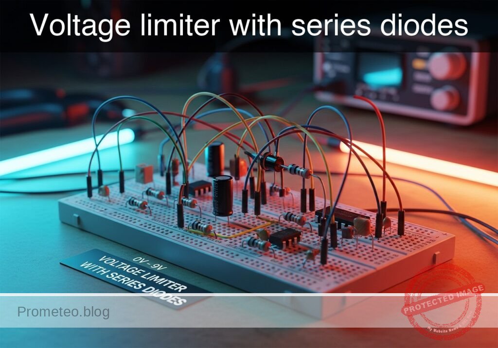
Practical case: Voltage limiter with series diodes

Voltage limiter with series diodes prototype (Maker Style)

Level: Basic – Build a circuit to clamp load voltage using diode forward drops.

Objective and use case

In this practical case, you will build a passive voltage limiter (clipper) circuit. By placing multiple silicon diodes in series parallel to the load, you will create a hard «ceiling» for the output voltage, preventing it from exceeding the sum of the forward voltage drops of the diodes.

  • Input protection: Prevents high voltage spikes from damaging sensitive microcontroller inputs (ADCs).
  • Simple regulation: Provides a crude but effective constant voltage reference without a Zener diode.
  • Signal conditioning: Used in audio circuits to create distortion or «fuzz» effects by clipping signal peaks.
  • Logical reference: Can be used to establish specific logic threshold levels in analog computing.

Expected outcome:
* When Input Voltage < ~2.1 V: The output voltage follows the input (minus minor resistive losses).
* When Input Voltage > ~2.1 V: The output voltage clamps and remains stable at approximately 2.1 V.
* The current through the diodes increases significantly once the threshold is reached.
* Target audience: Students and hobbyists learning about diode I-V characteristics.

Materials

  • V1: 0 V to 9 V Variable DC Power Supply, function: Input signal source.
  • R1: 1 kΩ resistor, function: Current limiting for the diodes and source protection.
  • R2: 10 kΩ resistor, function: Load resistor (simulating a downstream circuit).
  • D1: 1N4148 Silicon Diode, function: First voltage drop element (~0.7 V).
  • D2: 1N4148 Silicon Diode, function: Second voltage drop element (~0.7 V).
  • D3: 1N4148 Silicon Diode, function: Third voltage drop element (~0.7 V).

Wiring guide

Construct the circuit following these connections. The node names (e.g., VIN, VOUT, 0) refer to specific electrical points in the circuit. Node 0 represents the Ground (GND).

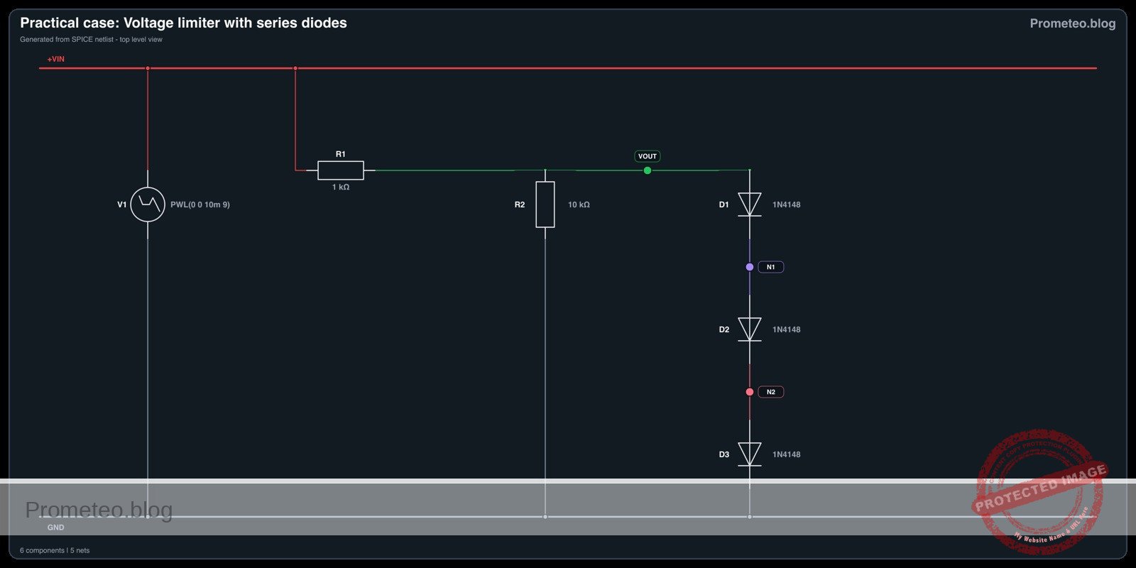
  • V1 (Source): Connect the positive terminal to node VIN and the negative terminal to node 0.
  • R1 (Limiter): Connect one pin to node VIN and the other pin to node VOUT.
  • R2 (Load): Connect one pin to node VOUT and the other pin to node 0.
  • D1: Connect the Anode to node VOUT and the Cathode to intermediate node N1.
  • D2: Connect the Anode to intermediate node N1 and the Cathode to intermediate node N2.
  • D3: Connect the Anode to intermediate node N2 and the Cathode to node 0.

Note: This creates a chain where D1, D2, and D3 are in series with each other, and that entire string is in parallel with R2.

Conceptual block diagram

Conceptual block diagram — Series Diode Limiter
Quick read: inputs → main block → output (actuator or measurement). This summarizes the ASCII schematic below.

Schematic

[ INPUT SOURCE ]              [ SERIES LIMITER ]                  [ OUTPUT NODE & BRANCHES ]

                                                                 /------> [ R2: 10 kΩ Load ] ---------> GND (0)
                                                                 |
[ V1: 0-9 V Variable ] --(VIN)--> [ R1: 1 kΩ Resistor ] --(VOUT)-->+
                                                                 |
                                                                 |        [ VOLTAGE CLAMP CHAIN ]
                                                                 |
                                                                 \------> [ D1: 1N4148 ] --(N1)-->+
                                                                                                  |
                                                                          [ D2: 1N4148 ] <--------+
                                                                          |
                                                                          +--(N2)--> [ D3: 1N4148 ] --> GND (0)
Schematic (ASCII)

Electrical diagram

Electrical diagram for practical case: Voltage limiter with series diodes
Generated from the validated SPICE netlist for this case.

🔒 This electrical diagram is premium. With the monthly membership (7-day free trial) you can unlock the complete didactic material and the print-ready PDF pack.🔓 See premium access plans

Measurements and tests

Follow these steps to validate the limiting behavior.

  1. Low Voltage Test (Below Threshold):

    • Set V1 to 1.0 V.
    • Measure the voltage at VOUT relative to GND.
    • Expected Result: VOUT should be approximately 0.9 V – 1.0 V (diodes are off/high impedance; R1 and R2 form a voltage divider).
  2. Transition Test (Near Threshold):

    • Set V1 to 2.5 V.
    • Measure the voltage at VOUT.
    • Expected Result: VOUT begins to lag behind VIN. Diodes start conducting. VOUT will likely be around 1.8 V to 2.0 V.
  3. Clamping Test (Above Threshold):

    • Set V1 to 9.0 V.
    • Measure the voltage at VOUT.
    • Expected Result: VOUT should be clamped at approximately 2.1 V to 2.2 V (3 diodes × ~0.7 V each). It will NOT reach 9 V.
  4. Transfer Curve Sweep:

    • Slowly increase V1 from 0 V to 9 V while monitoring VOUT.
    • Observe that VOUT rises linearly initially, then «knees» over and flattens out around 2.1 V.

SPICE netlist and simulation

Reference SPICE Netlist (ngspice) — excerptFull SPICE netlist (ngspice)

* Practical case: Voltage limiter with series diodes

* --- Power Supply / Input Signal ---
* V1: 0 V to 9 V Variable DC Power Supply
* Modeled as a linear ramp (PWL) from 0V to 9V over 10ms
* This allows the transient analysis to show the voltage limiting characteristic.
V1 VIN 0 PWL(0 0 10m 9)

* --- Resistors ---
* R1: 1 kΩ resistor (Current limiting)
* Connects VIN to VOUT
R1 VIN VOUT 1k

* R2: 10 kΩ resistor (Load)
* Connects VOUT to Ground (0)
R2 VOUT 0 10k

* --- Diodes ---
* Chain of 3 diodes in series, connected in parallel with the load (R2).
* This clamps VOUT to approximately 3 * 0.7V = 2.1V.
* ... (truncated in public view) ...

Copy this content into a .cir file and run with ngspice.

🔒 Part of this section is premium. With the monthly membership (7-day free trial) you can access the full content (materials, wiring, detailed build, validation, troubleshooting, variants and checklist) and download the complete print-ready PDF pack.

* Practical case: Voltage limiter with series diodes

* --- Power Supply / Input Signal ---
* V1: 0 V to 9 V Variable DC Power Supply
* Modeled as a linear ramp (PWL) from 0V to 9V over 10ms
* This allows the transient analysis to show the voltage limiting characteristic.
V1 VIN 0 PWL(0 0 10m 9)

* --- Resistors ---
* R1: 1 kΩ resistor (Current limiting)
* Connects VIN to VOUT
R1 VIN VOUT 1k

* R2: 10 kΩ resistor (Load)
* Connects VOUT to Ground (0)
R2 VOUT 0 10k

* --- Diodes ---
* Chain of 3 diodes in series, connected in parallel with the load (R2).
* This clamps VOUT to approximately 3 * 0.7V = 2.1V.

* D1: 1N4148 Silicon Diode
* Anode -> VOUT, Cathode -> N1
D1 VOUT N1 1N4148

* D2: 1N4148 Silicon Diode
* Anode -> N1, Cathode -> N2
D2 N1 N2 1N4148

* D3: 1N4148 Silicon Diode
* Anode -> N2, Cathode -> Ground (0)
D3 N2 0 1N4148

* --- Models ---
* Standard model for 1N4148 small signal diode
.model 1N4148 D (IS=2.682n N=1.836 RS=0.5664 BV=100 IBV=20n CJO=4p TT=11.54n)

* --- Simulation Directives ---
* Perform a transient analysis for 10ms (matching the input ramp duration)
* Step size 10us
.tran 10u 10m

* Calculate DC operating point
.op

* Output data for plotting/logging
.print tran V(VIN) V(VOUT) V(N1) V(N2)

.end

Simulation Results (Transient Analysis)

Simulation Results (Transient Analysis)
Show raw data table (2016 rows)
Index   time            v(vin)          v(vout)         v(n1)
0	0.000000e+00	0.000000e+00	-9.87864e-23	2.810146e-18
1	1.000000e-07	9.000000e-05	8.083682e-05	5.389121e-05
2	2.000000e-07	1.800000e-04	1.626418e-04	1.084279e-04
3	4.000000e-07	3.600000e-04	3.262751e-04	2.175167e-04
4	8.000000e-07	7.200000e-04	6.535424e-04	4.356949e-04
5	1.600000e-06	1.440000e-03	1.308076e-03	8.720508e-04
6	3.200000e-06	2.880000e-03	2.617144e-03	1.744763e-03
7	6.400000e-06	5.760000e-03	5.235279e-03	3.490186e-03
8	1.280000e-05	1.152000e-02	1.047155e-02	6.981032e-03
9	2.280000e-05	2.052000e-02	1.865321e-02	1.243547e-02
10	3.280000e-05	2.952000e-02	2.683486e-02	1.788991e-02
11	4.280000e-05	3.852000e-02	3.501650e-02	2.334434e-02
12	5.280000e-05	4.752000e-02	4.319814e-02	2.879876e-02
13	6.280000e-05	5.652000e-02	5.137976e-02	3.425317e-02
14	7.280000e-05	6.552000e-02	5.956137e-02	3.970758e-02
15	8.280000e-05	7.452000e-02	6.774297e-02	4.516198e-02
16	9.280000e-05	8.352000e-02	7.592455e-02	5.061637e-02
17	1.028000e-04	9.252000e-02	8.410612e-02	5.607075e-02
18	1.128000e-04	1.015200e-01	9.228768e-02	6.152512e-02
19	1.228000e-04	1.105200e-01	1.004692e-01	6.697948e-02
20	1.328000e-04	1.195200e-01	1.086507e-01	7.243383e-02
21	1.428000e-04	1.285200e-01	1.168323e-01	7.788817e-02
22	1.528000e-04	1.375200e-01	1.250137e-01	8.334250e-02
23	1.628000e-04	1.465200e-01	1.331952e-01	8.879681e-02
... (1992 more rows) ...


Reference SPICE netlist (ngspice)

* Practical case: Voltage limiter with series diodes

* --- Power Supply / Input Signal ---
* V1: 0 V to 9 V Variable DC Power Supply
* Modeled as a linear ramp (PWL) from 0V to 9V over 10ms
* This allows the transient analysis to show the voltage limiting characteristic.
V1 VIN 0 PWL(0 0 10m 9)

* --- Resistors ---
* R1: 1 kΩ resistor (Current limiting)
* Connects VIN to VOUT
R1 VIN VOUT 1k

* R2: 10 kΩ resistor (Load)
* Connects VOUT to Ground (0)
R2 VOUT 0 10k

* --- Diodes ---
* Chain of 3 diodes in series, connected in parallel with the load (R2).
* This clamps VOUT to approximately 3 * 0.7V = 2.1V.

* D1: 1N4148 Silicon Diode
* Anode -> VOUT, Cathode -> N1
D1 VOUT N1 1N4148

* D2: 1N4148 Silicon Diode
* Anode -> N1, Cathode -> N2
D2 N1 N2 1N4148

* D3: 1N4148 Silicon Diode
* Anode -> N2, Cathode -> Ground (0)
D3 N2 0 1N4148

* --- Models ---
* Standard model for 1N4148 small signal diode
.model 1N4148 D (IS=2.682n N=1.836 RS=0.5664 BV=100 IBV=20n CJO=4p TT=11.54n)

* --- Simulation Directives ---
* Perform a transient analysis for 10ms (matching the input ramp duration)
* Step size 10us
.tran 10u 10m

* Calculate DC operating point
.op

* Output data for plotting/logging
.print tran V(VIN) V(VOUT) V(N1) V(N2)

.end

Simulation Results (Transient Analysis)

Simulation Results (Transient Analysis)

Common mistakes and how to avoid them

  1. Reversing diode polarity: If diodes are connected Cathode-to-Anode (facing up towards positive), they will not conduct in forward bias. Solution: Ensure the band (Cathode) of D3 connects to Ground, and the arrows point from VOUT to Ground.
  2. Omitting R1: Connecting the source directly to the diode string without R1 causes a short circuit when V1 > 2.1 V, likely destroying the diodes. Solution: Always include a series resistor (R1) to drop the excess voltage.
  3. Using a low resistance load (R2): If R2 is very small (e.g., 100 Ω), it will dominate the circuit and reduce VOUT below the clamping threshold purely by voltage division. Solution: Ensure the load R2 is significantly larger than R1 (at least 10x larger) for sharp clamping action.

Troubleshooting

  • Symptom: VOUT equals VIN for the entire 0-9 V range.
    • Cause: The diode path is open.
    • Fix: Check for loose connections in the D1-D2-D3 string or a backwards diode blocking current.
  • Symptom: VOUT stays near 0 V even when VIN is increased.
    • Cause: Diodes are shorted or one diode is reversed and connected in parallel with the supply incorrectly (though R1 usually protects this).
    • Fix: Check diode orientation. If a diode is reversed parallel to the load, it clamps at -0.7 V (essentially 0 V in this setup).
  • Symptom: The clamping voltage is ~0.7 V or ~1.4 V instead of ~2.1 V.
    • Cause: One or two diodes are shorted or bypassed.
    • Fix: Verify that exactly three healthy diodes are in the series string.

Possible improvements and extensions

  1. Adjustable Clamp: Replace the fixed D1-D3 string with a Zener diode (e.g., 3.3 V or 5.1 V) to set a specific protection voltage with a single component.
  2. Visual Indication: Replace one of the standard diodes with a red LED. The clamp voltage will rise (LEDs drop ~1.8 V – 2.0 V), and the LED will light up when the input voltage exceeds the limit, acting as an «Overvoltage Warning.»

More Practical Cases on Prometeo.blog

Find this product and/or books on this topic on Amazon

Go to Amazon

As an Amazon Associate, I earn from qualifying purchases. If you buy through this link, you help keep this project running.

Quick Quiz

Question 1: What is the primary function of the circuit described in this practical case?


Question 2: How is the voltage 'ceiling' established in this specific circuit design?


Question 3: What happens to the output voltage when the input voltage exceeds approximately 2.1 V?


Question 4: What is the primary purpose of the resistor R1 (1 kΩ) in this circuit?


Question 5: Which component represents the downstream circuit or load in this experiment?


Question 6: What is the approximate forward voltage drop of a single standard silicon diode like the 1N4148?


Question 7: When used for input protection, what specific threat does this circuit mitigate?


Question 8: In the context of audio circuits, what effect does this clipping signal conditioning produce?


Question 9: How does the current flowing through the diodes behave once the voltage threshold is reached?


Question 10: To achieve a clamping threshold of ~2.1 V using silicon diodes (approx. 0.7 V drop each), how many are needed in series?


Carlos Núñez Zorrilla
Electronics & Computer Engineer

Telecommunications Electronics Engineer and Computer Engineer (official degrees in Spain).
Follow me:


Practical case: Reverse polarity protection

Reverse polarity protection prototype (Maker Style)

Level: Basic – Demonstrate how a diode protects a sensitive circuit (like a DC motor) if the battery is connected backwards.

Objective and use case

In this practical case, you will build a safety circuit that allows current to flow to a load (a DC motor) only when the battery is connected with the correct polarity.

  • Prevents damage to components: Essential for protecting polarized components like electrolytic capacitors and microcontrollers from exploding or burning out.
  • Automotive applications: Used in car electronics (ECUs, radios) to prevent damage if the car battery is installed incorrectly.
  • Consumer electronics: Protects toys and handheld devices where users might insert batteries backwards.

Expected outcome:
* Correct Polarity: The motor spins, and the voltage at the load is approximately 0.7 V lower than the battery voltage.
* Reverse Polarity: The motor remains completely off (0 V at the load), ensuring no reverse current damages the device.
* Voltage Drop: Measurement of the characteristic forward voltage drop (~0.6 V to 0.7 V) across the silicon diode.

Target audience: Hobbyists and basic electronics students.

Materials

  • V1: 9 V Battery or DC Power Supply, function: Main energy source.
  • D1: 1N4007 Rectifier Diode, function: Blocks current flow in reverse direction.
  • M1: 9 V DC Hobby Motor, function: The sensitive load being protected.
  • S1: SPST Toggle Switch (Optional), function: Master ON/OFF control.

Wiring guide

This circuit puts the diode in series with the positive rail of the power supply.

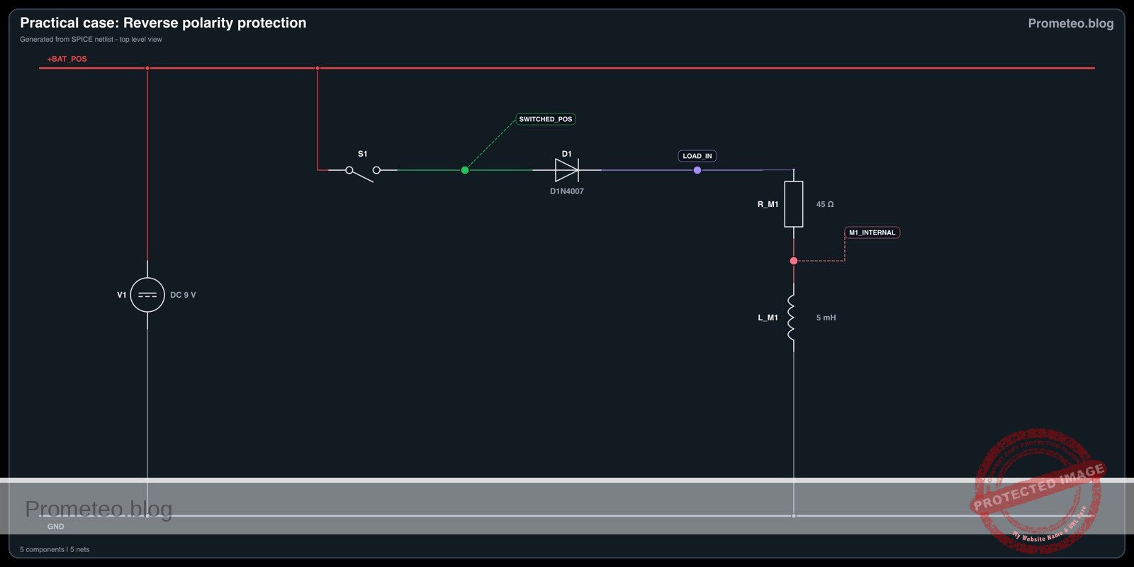
  • V1 (Positive Terminal) connects to node BAT_POS.
  • V1 (Negative Terminal) connects to node 0 (GND).
  • S1 (if used) connects between BAT_POS and node SWITCHED_POS. (If not used, connect BAT_POS directly to SWITCHED_POS).
  • D1 (Anode) connects to node SWITCHED_POS.
  • D1 (Cathode) connects to node LOAD_IN. (The striped band on the physical component marks the cathode).
  • M1 (Positive Terminal) connects to node LOAD_IN.
  • M1 (Negative Terminal) connects to node 0 (GND).

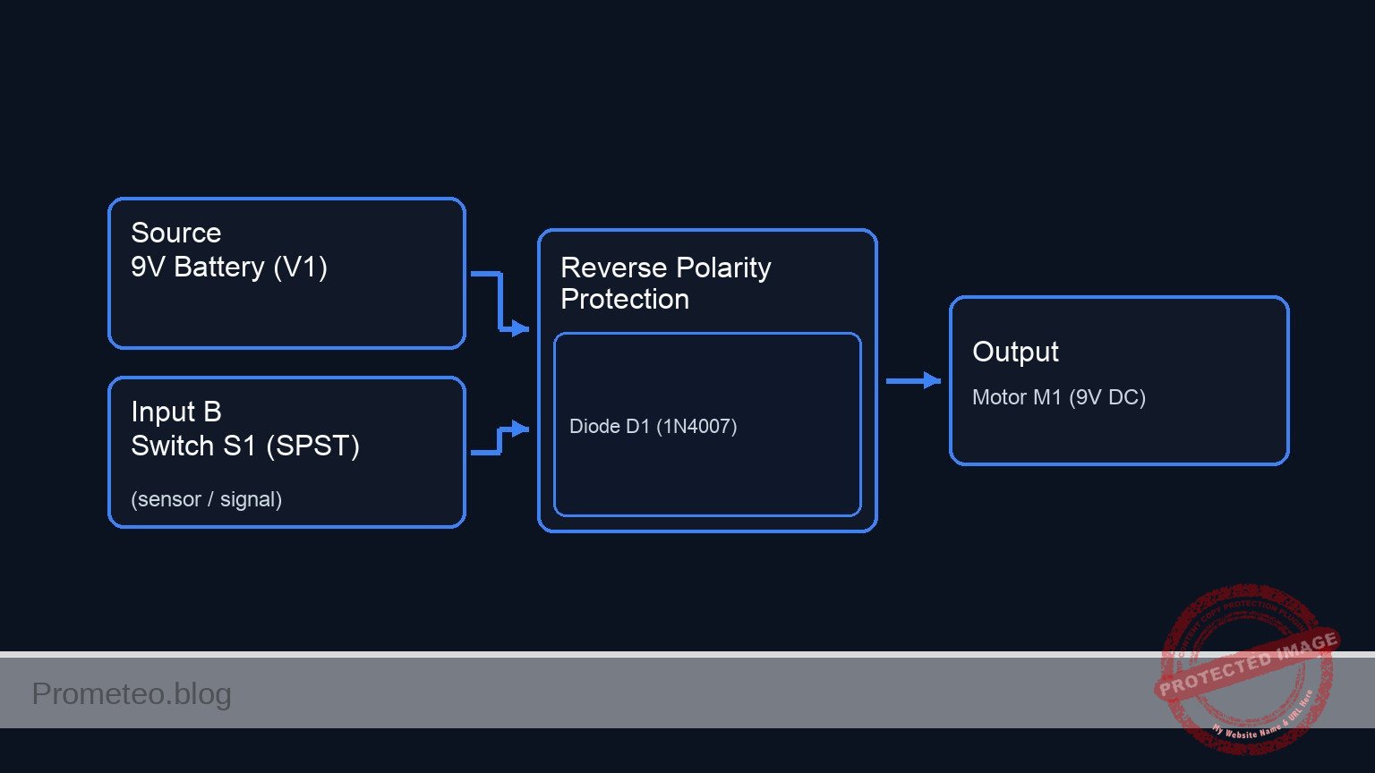
Conceptual block diagram

Conceptual block diagram — Reverse Polarity Protection
Quick read: inputs → main block → output (actuator or measurement). This summarizes the ASCII schematic below.

Schematic

[ POWER SOURCE ]              [ LOGIC / PROTECTION ]                 [ OUTPUT LOAD ]

+---------------------+       +-----------+        +--------------+       +--------------+
|   9 V Battery (V1)   |       | Switch S1 |        |   Diode D1   |       |   Motor M1   |
|      (Positive)     |------>|  (SPST)   |------->|   (1N4007)   |------>|   (9 V DC)    |-----> [ GND ]
+---------------------+   ^   +-----------+    ^   | Anode->Cath  |   ^   +--------------+
                          |                    |   +--------------+   |
                      (BAT_POS)          (SWITCHED_POS)           (LOAD_IN)
Schematic (ASCII)

Electrical diagram

Electrical diagram for case: Reverse polarity protection
Generated from the validated SPICE netlist for this case.

🔒 This electrical diagram is premium. With the monthly membership (7-day free trial) you can unlock the complete didactic material and the print-ready PDF pack.🔓 See premium access plans

Measurements and tests

To validate the protection, perform the following steps using a multimeter:

  1. Forward Bias Test (Normal Operation):

    • Connect V1 correctly (Positive to Anode side).
    • Observe: The motor M1 spins.
    • Measure: Place the red probe on LOAD_IN and the black probe on 0 (GND). Expect a reading of approx. 8.3 V to 8.4 V (9 V input minus the diode drop).
  2. Diode Drop Measurement:

    • With the circuit powered ON, place probes across D1 (Red on SWITCHED_POS, Black on LOAD_IN).
    • Result: You should read approximately 0.6 V to 0.7 V. This confirms the diode is conducting.
  3. Reverse Bias Test (Simulation of Error):

    • Disconnect V1 and reverse the connections (Positive to GND, Negative to the input of the switch/diode).
    • Observe: The motor M1 does not spin. It is completely safe.
    • Measure: Place the red probe on LOAD_IN and the black probe on the battery negative (now at the top). The reading should be 0 V. Current is blocked.

SPICE netlist and simulation

Reference SPICE Netlist (ngspice) — excerptFull SPICE netlist (ngspice)

* TITLE: Practical case: Reverse polarity protection

* --- Bill of Materials & Component Models ---

* V1: 9 V Battery or DC Power Supply
* Function: Main energy source
* Connected between BAT_POS and GND (0)
V1 BAT_POS 0 DC 9

* S1: SPST Toggle Switch
* Function: Master ON/OFF control
* Connected between BAT_POS and SWITCHED_POS
* Modeled as a voltage-controlled switch driven by a stimulus source to simulate user action.
S1 BAT_POS SWITCHED_POS CTRL_NODE 0 SW_MODEL
.model SW_MODEL SW(Vt=2.5 Ron=0.1 Roff=100Meg)

* Stimulus for S1 (User pressing the switch)
* Switch is OPEN (0V) initially, closes (5V) at 100us.
V_S1_ACT CTRL_NODE 0 PULSE(0 5 100u 1u 1u 10m 20m)

* ... (truncated in public view) ...

Copy this content into a .cir file and run with ngspice.

🔒 Part of this section is premium. With the monthly membership (7-day free trial) you can access the full content (materials, wiring, detailed build, validation, troubleshooting, variants and checklist) and download the complete print-ready PDF pack.

* TITLE: Practical case: Reverse polarity protection

* --- Bill of Materials & Component Models ---

* V1: 9 V Battery or DC Power Supply
* Function: Main energy source
* Connected between BAT_POS and GND (0)
V1 BAT_POS 0 DC 9

* S1: SPST Toggle Switch
* Function: Master ON/OFF control
* Connected between BAT_POS and SWITCHED_POS
* Modeled as a voltage-controlled switch driven by a stimulus source to simulate user action.
S1 BAT_POS SWITCHED_POS CTRL_NODE 0 SW_MODEL
.model SW_MODEL SW(Vt=2.5 Ron=0.1 Roff=100Meg)

* Stimulus for S1 (User pressing the switch)
* Switch is OPEN (0V) initially, closes (5V) at 100us.
V_S1_ACT CTRL_NODE 0 PULSE(0 5 100u 1u 1u 10m 20m)

* D1: 1N4007 Rectifier Diode
* Function: Blocks current flow in reverse direction
* Anode -> SWITCHED_POS, Cathode -> LOAD_IN
D1 SWITCHED_POS LOAD_IN D1N4007
* Standard generic model for 1N4007
.model D1N4007 D(IS=7.03n RS=0.034 N=1.8 BV=1000 IBV=5u CJO=10p VJ=0.7 M=0.5 TT=100n)

* M1: 9 V DC Hobby Motor
* Function: The sensitive load being protected
* Connected between LOAD_IN and GND (0)
* Modeled as a Series Resistor (winding resistance) and Inductor
R_M1 LOAD_IN M1_INTERNAL 45
L_M1 M1_INTERNAL 0 5m

* --- Analysis & Output Directives ---

* Transient analysis to observe the switch turning on and voltage drop across diode
.tran 10u 2m

* Print directives for ngspice batch mode
.print tran V(BAT_POS) V(SWITCHED_POS) V(LOAD_IN)

* Operating point analysis
.op

.end

Simulation Results (Transient Analysis)

Simulation Results (Transient Analysis)
Show raw data table (233 rows)
Index   time            v(bat_pos)      v(switched_pos) v(load_in)
0	0.000000e+00	9.000000e+00	1.216207e-01	3.995271e-06
1	1.000000e-07	9.000000e+00	1.216207e-01	3.995280e-06
2	2.000000e-07	9.000000e+00	1.216207e-01	3.995265e-06
3	4.000000e-07	9.000000e+00	1.216207e-01	3.995282e-06
4	8.000000e-07	9.000000e+00	1.216207e-01	3.995257e-06
5	1.600000e-06	9.000000e+00	1.216207e-01	3.995290e-06
6	3.200000e-06	9.000000e+00	1.216207e-01	3.995250e-06
7	6.400000e-06	9.000000e+00	1.216207e-01	3.995292e-06
8	1.280000e-05	9.000000e+00	1.216207e-01	3.995249e-06
9	2.280000e-05	9.000000e+00	1.216207e-01	3.995292e-06
10	3.280000e-05	9.000000e+00	1.216207e-01	3.995249e-06
11	4.280000e-05	9.000000e+00	1.216207e-01	3.995292e-06
12	5.280000e-05	9.000000e+00	1.216207e-01	3.995249e-06
13	6.280000e-05	9.000000e+00	1.216207e-01	3.995292e-06
14	7.280000e-05	9.000000e+00	1.216207e-01	3.995249e-06
15	8.280000e-05	9.000000e+00	1.216207e-01	3.995292e-06
16	9.280000e-05	9.000000e+00	1.216207e-01	3.995249e-06
17	1.000000e-04	9.000000e+00	1.216207e-01	3.995292e-06
18	1.001000e-04	9.000000e+00	1.216207e-01	3.995267e-06
19	1.002600e-04	9.000000e+00	1.216207e-01	3.995284e-06
20	1.003075e-04	9.000000e+00	1.216207e-01	3.995227e-06
21	1.003906e-04	9.000000e+00	1.216207e-01	3.995299e-06
22	1.004136e-04	9.000000e+00	1.216207e-01	3.995334e-06
23	1.004539e-04	9.000000e+00	1.216207e-01	3.995198e-06
... (209 more rows) ...


Reference SPICE netlist (ngspice)

* TITLE: Practical case: Reverse polarity protection

* --- Bill of Materials & Component Models ---

* V1: 9 V Battery or DC Power Supply
* Function: Main energy source
* Connected between BAT_POS and GND (0)
V1 BAT_POS 0 DC 9

* S1: SPST Toggle Switch
* Function: Master ON/OFF control
* Connected between BAT_POS and SWITCHED_POS
* Modeled as a voltage-controlled switch driven by a stimulus source to simulate user action.
S1 BAT_POS SWITCHED_POS CTRL_NODE 0 SW_MODEL
.model SW_MODEL SW(Vt=2.5 Ron=0.1 Roff=100Meg)

* Stimulus for S1 (User pressing the switch)
* Switch is OPEN (0V) initially, closes (5V) at 100us.
V_S1_ACT CTRL_NODE 0 PULSE(0 5 100u 1u 1u 10m 20m)

* D1: 1N4007 Rectifier Diode
* Function: Blocks current flow in reverse direction
* Anode -> SWITCHED_POS, Cathode -> LOAD_IN
D1 SWITCHED_POS LOAD_IN D1N4007
* Standard generic model for 1N4007
.model D1N4007 D(IS=7.03n RS=0.034 N=1.8 BV=1000 IBV=5u CJO=10p VJ=0.7 M=0.5 TT=100n)

* M1: 9 V DC Hobby Motor
* Function: The sensitive load being protected
* Connected between LOAD_IN and GND (0)
* Modeled as a Series Resistor (winding resistance) and Inductor
R_M1 LOAD_IN M1_INTERNAL 45
L_M1 M1_INTERNAL 0 5m

* --- Analysis & Output Directives ---

* Transient analysis to observe the switch turning on and voltage drop across diode
.tran 10u 2m

* Print directives for ngspice batch mode
.print tran V(BAT_POS) V(SWITCHED_POS) V(LOAD_IN)

* Operating point analysis
.op

.end

Simulation Results (Transient Analysis)

Simulation Results (Transient Analysis)

Common mistakes and how to avoid them

  1. Installing the diode backwards: The circuit will not work even with the correct battery polarity. Always ensure the silver band (cathode) points toward the load (M1).
  2. Using a signal diode for high loads: Using a small 1N4148 for a high-current motor may cause the diode to overheat and fail. Use a 1N400x series diode (1 A rating) for motors.
  3. Ignoring voltage drop: Students often forget that the diode «eats» about 0.7 V. If your load requires exactly 9 V, supplying 9 V through a diode might result in under-performance (8.3 V).

Troubleshooting

  • Symptom: Motor runs slower than expected.
    • Cause: The voltage drop across the diode reduces the effective voltage at the motor.
    • Fix: Increase the supply voltage slightly or use a Schottky diode.
  • Symptom: Diode gets very hot.
    • Cause: The motor draws more current than the diode is rated for.
    • Fix: Check the motor’s current draw and replace D1 with a higher amperage diode (e.g., 1N5408 for 3 A).
  • Symptom: Motor works in both battery orientations.
    • Cause: The diode has failed short (internal damage) or is bypassed by a wire.
    • Fix: Test the diode with the «Diode Check» function on a multimeter; replace if it conducts in both directions.

Possible improvements and extensions

  1. Schottky Diode Upgrade: Replace the 1N4007 with a 1N5817 (Schottky). Measure the voltage drop again; it should be lower (~0.3 V), making the circuit more efficient.
  2. Full Bridge Rectifier: Replace the single diode with a bridge rectifier consisting of 4 diodes. This allows the device to work regardless of polarity (auto-correction) rather than just blocking the wrong polarity.

More Practical Cases on Prometeo.blog

        <div class="amazon-affiliate">
          <p><strong>Find this product and/or books on this topic on Amazon</strong></p>
          <p><a class="amazon-affiliate-btn" href="https://amzn.to/4mt8r4C" target="_blank" rel="nofollow sponsored noopener">Go to Amazon</a></p>
          <p class="amazon-affiliate-disclaimer">As an Amazon Associate, I earn from qualifying purchases. If you buy through this link, you help keep this project running.</p>
        </div>

Quick Quiz

Question 1: What is the primary function of the diode in this circuit?


Question 2: What happens to the DC motor if the battery is connected with reverse polarity in this circuit?


Question 3: Which component is typically identified as 'D1' in this type of circuit?


Question 4: What is the approximate voltage drop expected across the silicon diode when the polarity is correct?


Question 5: Why is this circuit important for components like electrolytic capacitors?


Question 6: If the battery voltage is 9 V and the diode drop is 0.7 V, what is the approximate voltage at the load?


Question 7: How is the diode typically connected in this protection circuit?


Question 8: Which of the following is a listed use case for this circuit?


Question 9: What role does the battery (often labeled V1) play in this circuit?


Question 10: Who is the stated target audience for this practical case?


Carlos Núñez Zorrilla
Electronics & Computer Engineer

Telecommunications Electronics Engineer and Computer Engineer (official degrees in Spain).

Follow me:


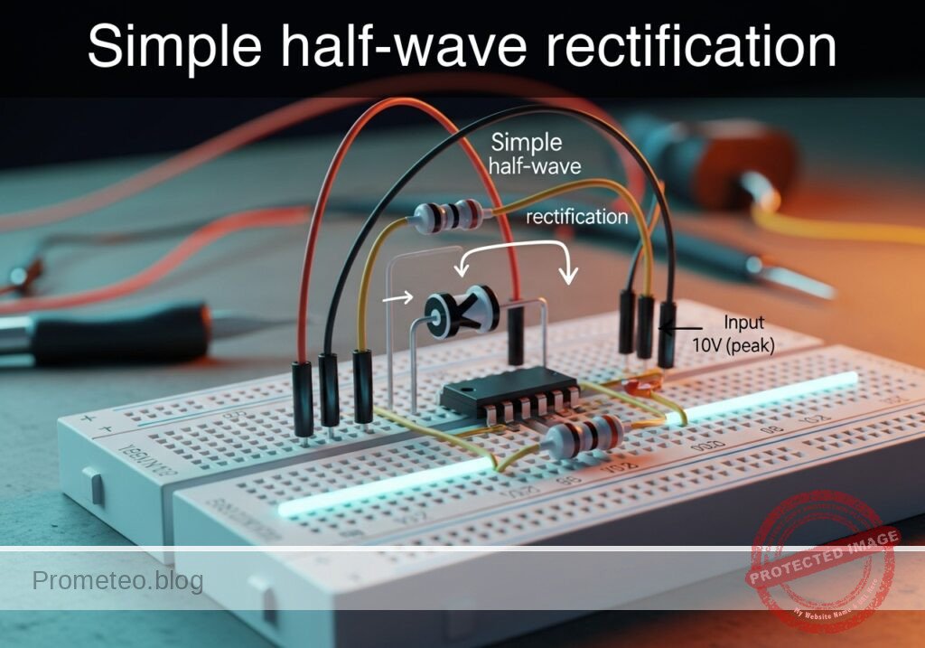
Practical case: Simple half-wave rectification

Simple half-wave rectification prototype (Maker Style)

Level: Basic. Visualizing how a diode converts AC to pulsating DC by removing the negative half-cycle.

Objective and use case

You will build a fundamental analog circuit that uses a single semiconductor diode to block the negative portion of an alternating current (AC) signal, passing only the positive portion to a resistive load.

Why it is useful:
* Power conversion: It represents the first stage in converting AC mains power to DC for electronic devices.
* Signal demodulation: Used in AM radios to extract audio signals from radio frequency carriers (envelope detector).
* Polarity protection: Similar logic prevents damage to DC circuits if batteries are inserted backward.

Expected outcome:
* Input Signal: A complete sine wave swinging between positive and negative voltages (e.g., +10 V to -10 V).
* Output Signal: A pulsating waveform showing only the positive «humps» of the sine wave; the voltage sits at 0 V during the negative cycle.
* Voltage Drop: The peak output voltage will be approximately 0.7 V lower than the input peak due to the silicon diode forward voltage drop.
* Frequency: The output frequency remains identical to the input frequency.

Target audience and level: Students and hobbyists learning basic analog components.

Materials

  • V1: 10 V (peak), 60 Hz AC voltage source (sine wave), function: main power input.
  • D1: 1N4007 (or 1N4148), function: rectifier diode.
  • R1: 1 kΩ resistor, function: resistive load.

Wiring guide

This guide defines the connections between components using specific node names (VIN, VOUT, 0).

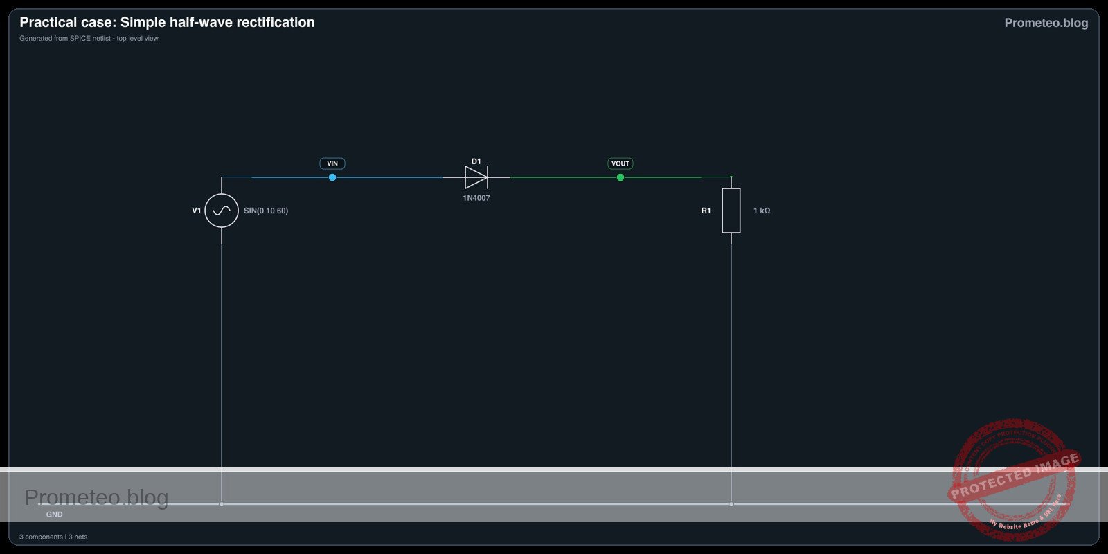
  • V1 (Source): Connect the positive terminal to node VIN and the negative terminal to node 0 (GND).
  • D1 (Diode): Connect the Anode to node VIN and the Cathode (marked with a stripe) to node VOUT.
  • R1 (Load): Connect one terminal to node VOUT and the other terminal to node 0 (GND).

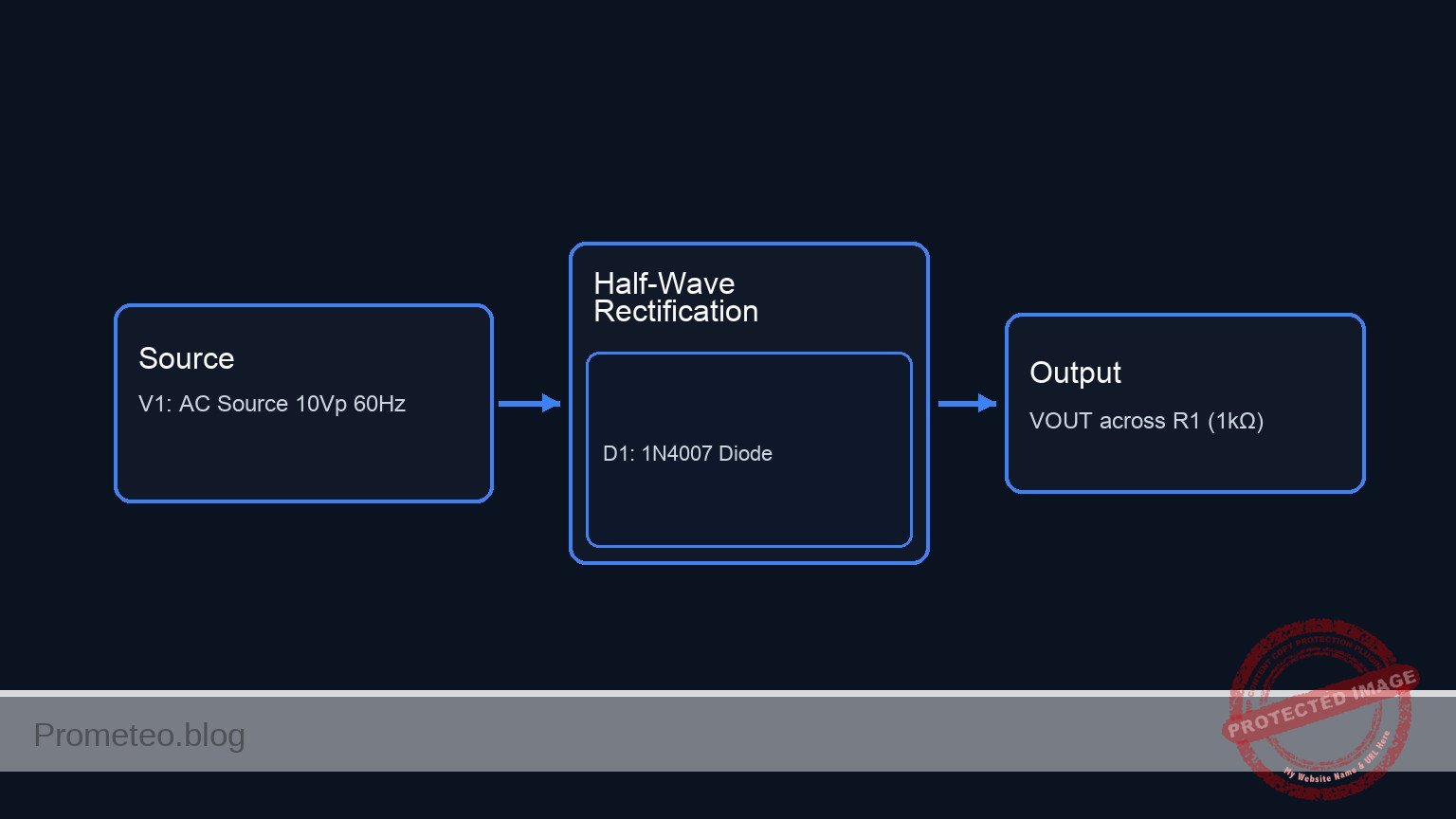
Conceptual block diagram

Conceptual block diagram — Half-Wave Rectification
Quick read: inputs → main block → output (actuator or measurement). This summarizes the ASCII schematic below.

Schematic

[ SOURCE / INPUT ]             [ RECTIFICATION ]               [ LOAD / OUTPUT ]

[ V1: AC Source    ]           +----------------------+           [ R1: Resistor   ]
[ 10 V Peak, 60Hz   ] --(VIN)-->| Anode (A) -> Cathode | --(VOUT)--> [ 1 kΩ         ] --> GND
                               | D1: 1N4007           |
                               +----------------------+
Schematic (ASCII)

Electrical diagram

Electrical diagram for case: Simple half-wave rectification
Generated from the validated SPICE netlist for this case.

🔒 This electrical diagram is premium. With the monthly membership (7-day free trial) you can unlock the complete didactic material and the print-ready PDF pack.🔓 See premium access plans

Measurements and tests

To validate the circuit, you will need a dual-channel oscilloscope or a simulation tool.

  1. Setup Probes:
    • Connect Channel A (Yellow) to VIN to monitor the source.
    • Connect Channel B (Blue) to VOUT to monitor the voltage across the resistor.
    • Ensure the ground clips of both probes are connected to node 0 (GND).
  2. Visual Inspection:
    • Observe that VIN is a full sine wave centered at 0 V.
    • Observe that VOUT follows VIN during the positive cycle but stays flat at 0 V during the negative cycle.
  3. Cursor Measurement:
    • Measure the peak voltage of VIN (e.g., 10.0 V).
    • Measure the peak voltage of VOUT. It should be approximately 9.3 V.
    • Calculate the difference (Vin – Vout). This confirms the roughly 0.7 V forward voltage drop of the silicon diode.

SPICE netlist and simulation

Reference SPICE Netlist (ngspice) — excerptFull SPICE netlist (ngspice)

* Practical case: Simple half-wave rectification

* --- Circuit Description ---
* V1 (Source): 10V Peak, 60Hz Sine Wave
* D1 (Diode): 1N4007 Rectifier
* R1 (Load): 1k Ohm Resistor

* --- Components ---

* V1: Main power input
* Connected: Positive -> VIN, Negative -> 0 (GND)
* Syntax: SIN(Voffset Vamp Freq)
V1 VIN 0 SIN(0 10 60)

* D1: Rectifier diode (1N4007)
* Connected: Anode -> VIN, Cathode -> VOUT
D1 VIN VOUT 1N4007

* R1: Resistive load
* Connected: VOUT -> 0 (GND)
* ... (truncated in public view) ...

Copy this content into a .cir file and run with ngspice.

🔒 Part of this section is premium. With the monthly membership (7-day free trial) you can access the full content (materials, wiring, detailed build, validation, troubleshooting, variants and checklist) and download the complete print-ready PDF pack.

* Practical case: Simple half-wave rectification

* --- Circuit Description ---
* V1 (Source): 10V Peak, 60Hz Sine Wave
* D1 (Diode): 1N4007 Rectifier
* R1 (Load): 1k Ohm Resistor

* --- Components ---

* V1: Main power input
* Connected: Positive -> VIN, Negative -> 0 (GND)
* Syntax: SIN(Voffset Vamp Freq)
V1 VIN 0 SIN(0 10 60)

* D1: Rectifier diode (1N4007)
* Connected: Anode -> VIN, Cathode -> VOUT
D1 VIN VOUT 1N4007

* R1: Resistive load
* Connected: VOUT -> 0 (GND)
R1 VOUT 0 1k

* --- Models ---
* Standard model for 1N4007 Diode
.model 1N4007 D (IS=7.69n RS=0.042 N=1.45 BV=1000 IBV=5u CJO=14.2p VJ=0.5 M=0.333 TT=4.32u)

* --- Analysis Commands ---
* Transient analysis
* Frequency is 60Hz (Period ~16.67ms).
* Simulate for 50ms to capture approximately 3 full cycles.
.tran 0.1ms 50ms

* Operating Point for initial check
.op

* --- Output Directives ---
* Print input voltage and rectified output voltage
.print tran V(VIN) V(VOUT)

.end

Simulation Results (Transient Analysis)

Simulation Results (Transient Analysis)
Show raw data table (515 rows)
Index   time            v(vin)          v(vout)
0	0.000000e+00	0.000000e+00	-2.01593e-21
1	1.000000e-06	3.769911e-03	5.704546e-05
2	2.000000e-06	7.539822e-03	5.927562e-05
3	4.000000e-06	1.507964e-02	6.305993e-05
4	8.000000e-06	3.015924e-02	7.111847e-05
5	1.600000e-05	6.031821e-02	1.021853e-04
6	3.200000e-05	1.206342e-01	3.070797e-04
7	5.378437e-05	2.027484e-01	2.167324e-03
8	7.424258e-05	2.798514e-01	1.250260e-02
9	9.741093e-05	3.671480e-01	4.715921e-02
10	1.262516e-04	4.757778e-01	1.182339e-01
11	1.839330e-04	6.928557e-01	2.983890e-01
12	2.467131e-04	9.287461e-01	5.130162e-01
13	3.467131e-04	1.303359e+00	8.676123e-01
14	4.467131e-04	1.676120e+00	1.226655e+00
15	5.467131e-04	2.046499e+00	1.587509e+00
16	6.467131e-04	2.413969e+00	1.947514e+00
17	7.467131e-04	2.778010e+00	2.305173e+00
18	8.467131e-04	3.138102e+00	2.659882e+00
19	9.467131e-04	3.493735e+00	3.010809e+00
20	1.046713e-03	3.844404e+00	3.357375e+00
21	1.146713e-03	4.189609e+00	3.698904e+00
22	1.246713e-03	4.528861e+00	4.034877e+00
23	1.346713e-03	4.861677e+00	4.364712e+00
... (491 more rows) ...


Reference SPICE netlist (ngspice)

* Practical case: Simple half-wave rectification

* --- Circuit Description ---
* V1 (Source): 10V Peak, 60Hz Sine Wave
* D1 (Diode): 1N4007 Rectifier
* R1 (Load): 1k Ohm Resistor

* --- Components ---

* V1: Main power input
* Connected: Positive -> VIN, Negative -> 0 (GND)
* Syntax: SIN(Voffset Vamp Freq)
V1 VIN 0 SIN(0 10 60)

* D1: Rectifier diode (1N4007)
* Connected: Anode -> VIN, Cathode -> VOUT
D1 VIN VOUT 1N4007

* R1: Resistive load
* Connected: VOUT -> 0 (GND)
R1 VOUT 0 1k

* --- Models ---
* Standard model for 1N4007 Diode
.model 1N4007 D (IS=7.69n RS=0.042 N=1.45 BV=1000 IBV=5u CJO=14.2p VJ=0.5 M=0.333 TT=4.32u)

* --- Analysis Commands ---
* Transient analysis
* Frequency is 60Hz (Period ~16.67ms).
* Simulate for 50ms to capture approximately 3 full cycles.
.tran 0.1ms 50ms

* Operating Point for initial check
.op

* --- Output Directives ---
* Print input voltage and rectified output voltage
.print tran V(VIN) V(VOUT)

.end

Simulation Results (Transient Analysis)

Simulation Results (Transient Analysis)

Common mistakes and how to avoid them

  1. Reversing the diode:
    • Error: The diode is installed with the cathode pointing toward the source.
    • Result: The circuit produces negative voltage pulses instead of positive ones.
    • Solution: Verify the stripe (cathode) points toward the load resistor.
  2. Ignoring power ratings:
    • Error: Using a very small resistor (e.g., 10 Ω) with a standard 1/4W resistor.
    • Result: The resistor overheats and burns.
    • Solution: Calculate power (P = V^2 / R) or use a resistor value like 1 kΩ or higher for demonstration purposes.
  3. Floating Ground:
    • Error: Measuring VOUT without a common ground reference between the source and the oscilloscope.
    • Result: Noisy or floating signals on the screen.
    • Solution: Ensure all grounds (Source, Resistor, Oscilloscope) are tied to node 0.

Troubleshooting

  • Symptom: No output voltage (0 V flatline).
    • Cause: Diode is open (blown) or disconnected.
    • Fix: Check continuity with a multimeter; replace the diode.
  • Symptom: Output is identical to Input (full sine wave).
    • Cause: Diode is shorted internally.
    • Fix: Replace the diode; a shorted diode acts like a wire.
  • Symptom: Output peak is significantly lower than expected (e.g., 5 V drop).
    • Cause: High internal resistance of the source or an incorrect component (e.g., using a Zener diode in reverse breakdown).
    • Fix: Verify the diode part number is a standard rectifier (1N400x series).

Possible improvements and extensions

  1. Filter Capacitor: Connect a capacitor (e.g., 10 µF) in parallel with R1 to observe how the capacitor fills in the gaps between pulses, smoothing the DC output.
  2. Full-Wave Bridge: Replace the single diode with four diodes (bridge configuration) to utilize both the positive and negative halves of the AC cycle, improving efficiency.

More Practical Cases on Prometeo.blog

Find this product and/or books on this topic on Amazon

Go to Amazon

As an Amazon Associate, I earn from qualifying purchases. If you buy through this link, you help keep this project running.

Quick Quiz

Question 1: What is the primary function of the semiconductor diode in this circuit?


Question 2: What is the expected shape of the output signal?


Question 3: How does the output frequency compare to the input frequency in this half-wave rectifier?


Question 4: Why is the peak output voltage slightly lower than the input peak voltage?


Question 5: Approximately how much voltage is typically dropped across a standard silicon diode?


Question 6: In a standard schematic for this circuit, which component typically acts as the load?


Question 7: What happens to the voltage at the output during the negative cycle of the input?


Question 8: Which of the following is a practical use case for this type of circuit mentioned in the text?


Question 9: To allow positive current to flow from the source to the load, how should the diode be oriented?


Question 10: If the input signal swings between +10 V and -10 V, what is the approximate peak output voltage?


Carlos Núñez Zorrilla
Electronics & Computer Engineer

Telecommunications Electronics Engineer and Computer Engineer (official degrees in Spain).
Follow me:


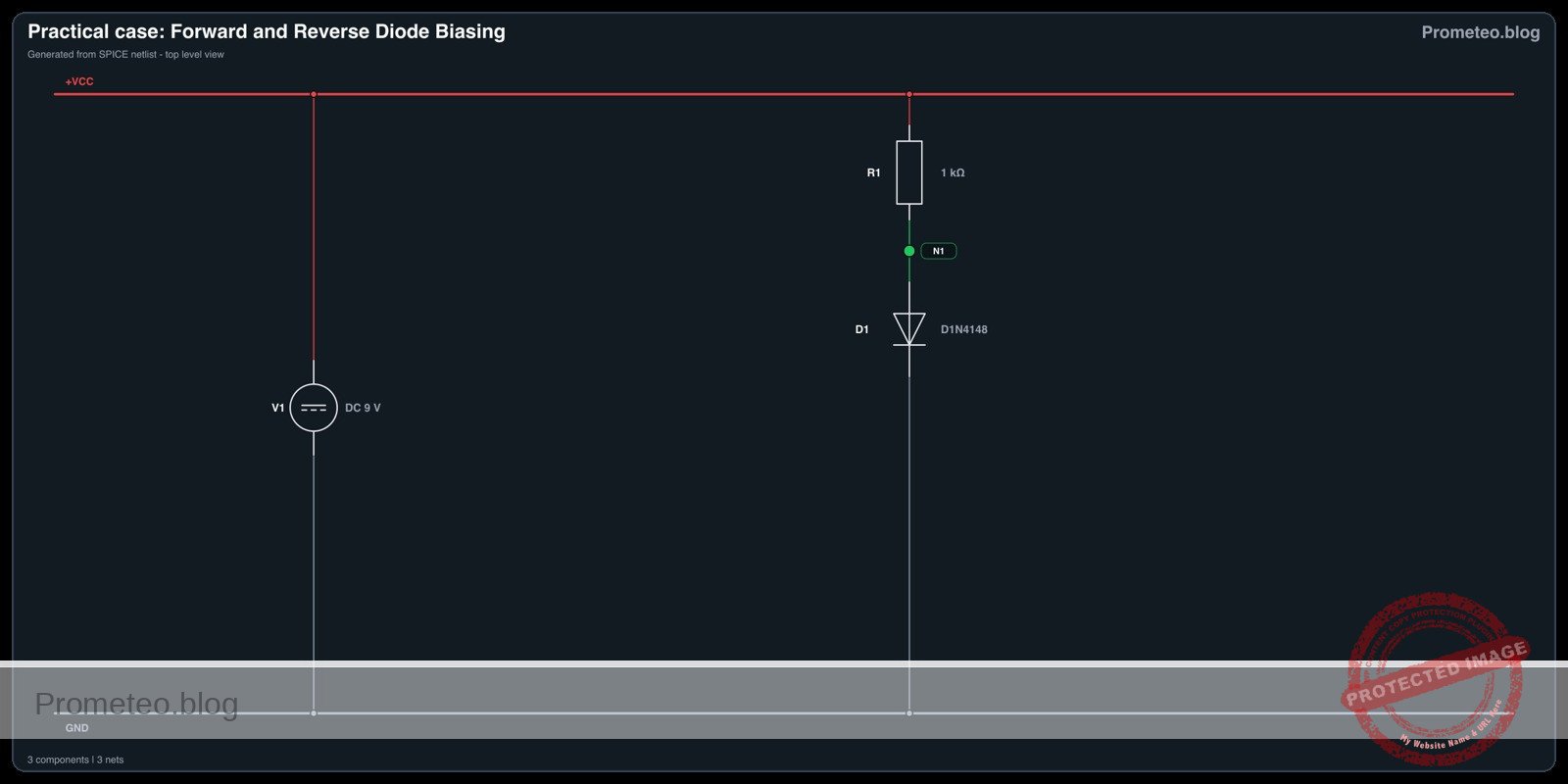
Practical case: Forward and Reverse Diode Biasing

Forward and Reverse Diode Biasing prototype (Maker Style)

Level: Basic. Verify the diode’s behavior as a unidirectional switch by measuring current and voltage in both polarities.

Objective and use case

In this experiment, you will build a simple series circuit consisting of a DC voltage source, a current-limiting resistor, and a silicon diode. You will measure the voltage drop across the diode and the current flowing through the circuit to confirm how the component blocks or conducts electricity based on its orientation.

  • Reverse polarity protection: Prevents damage to sensitive electronics if a battery is inserted backwards.
  • AC to DC Rectification: Converts alternating current into direct current in power supplies.
  • Signal clipping: Limits voltage levels to protect downstream components in communication circuits.
  • Logic implementation: Forms the basis of DTL (Diode-Transistor Logic) gates.

Expected outcome:
* Forward Bias: The diode conducts current; voltage across the diode (VD) stays near 0.7 V.
* Reverse Bias: The diode blocks current (I ≈ 0 A); voltage across the diode equals the supply voltage (Vsupply).
* Unidirectional flow: Confirmation that electrons only flow effectively in one direction (Anode to Cathode).

Target audience: Students and beginners in basic analog electronics.

Materials

  • V1: 9 V DC supply (battery or bench power supply).
  • R1: 1 kΩ resistor, function: current limiting and current sensing.
  • D1: 1N4148 silicon diode (or 1N4007), function: Device Under Test (DUT).
  • Multimeter: Digital multimeter, function: measuring DC voltage and DC current.

Wiring guide

This guide describes the Forward Bias configuration. The nodes are defined as VCC (9 V), N1 (junction), and 0 (GND).

  • V1: Connect the positive terminal to node VCC and the negative terminal to node 0.
  • R1: Connect one leg to node VCC and the other leg to node N1.
  • D1: Connect the Anode (side without the stripe) to node N1 and the Cathode (side with the stripe) to node 0.

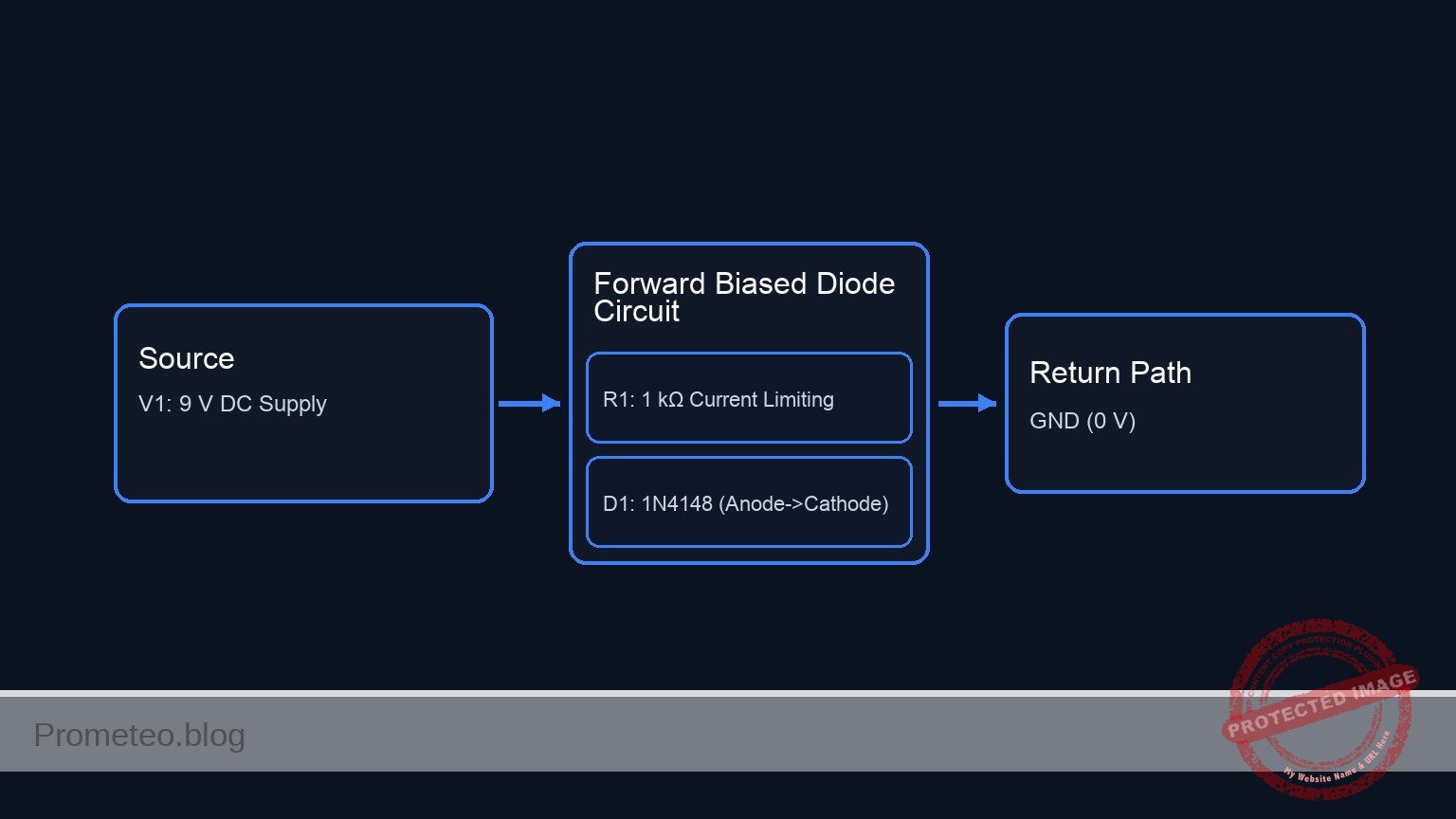
Conceptual block diagram

Conceptual block diagram — Forward Biased Diode Circuit
Quick read: inputs → main block → output (actuator or measurement). This summarizes the ASCII schematic below.

Schematic

[ POWER SOURCE ]               [ CIRCUIT PROCESSING ]                [ RETURN PATH ]

[ V1: 9 V DC Supply ] --(+9 V)--> [ R1: 1 kΩ Resistor ] --(Node N1)--> [ D1: 1N4148 Diode ] --(0 V)--> [ GND ]
                                (Current Limiting)    (Measurement)    (Anode -> Cathode)
                                                                        (Forward Biased)
Schematic (ASCII)

Electrical diagram

Electrical diagram for case: Forward and Reverse Diode Biasing
Generated from the validated SPICE netlist for this case.

🔒 This electrical diagram is premium. With the monthly membership (7-day free trial) you can unlock the complete didactic material and the print-ready PDF pack.🔓 See premium access plans

Measurements and tests

To validate the diode behavior, perform the following measurements using the multimeter.

1. Forward Bias Test (Anode to Positive)
* Voltage Measurement (VD): Set the multimeter to DC Volts. Place the red probe on the Anode (Node N1) and the black probe on the Cathode (Node 0).
* Result: You should read approximately 0.6 V to 0.7 V.
* Current Measurement (ID): Set the multimeter to DC mA. Break the circuit between R1 and D1, and insert the multimeter in series.
* Result: Using Ohm’s Law (I = (Vsource – VD) / R1), the current should be approximately 8.3 mA.

2. Reverse Bias Test (Cathode to Positive)
* Re-wiring: Disconnect D1, flip it 180 degrees, and reconnect it. Now the Cathode (stripe) connects to N1 and the Anode connects to 0.
* Voltage Measurement (VD): Measure across the diode again.
* Result: You should read a value very close to the source voltage (9 V), indicating the diode is acting as an open switch.
* Current Measurement (ID): Measure the current in the loop.
* Result: The reading should be 0 mA (or negligible leakage current in the nano-amp range).

SPICE netlist and simulation

Reference SPICE Netlist (ngspice) — excerptFull SPICE netlist (ngspice)

* Practical case: Forward and Reverse Diode Biasing
* Based on Wiring Guide: Forward Bias Configuration

* --- Power Supply ---
* V1: 9 V DC supply connected between VCC and GND (Node 0)
V1 VCC 0 DC 9

* --- Components ---
* R1: 1 kΩ resistor between VCC and Node N1
R1 VCC N1 1k

* D1: 1N4148 Diode
* Anode connected to N1, Cathode connected to GND (0)
D1 N1 0 D1N4148

* --- Models ---
* Standard 1N4148 Model
.model D1N4148 D (IS=2.682n N=1.836 RS=0.5664 BV=100 IBV=100p CJO=4p TT=11.54n)

* --- Analysis Directives ---
* ... (truncated in public view) ...

Copy this content into a .cir file and run with ngspice.

🔒 Part of this section is premium. With the monthly membership (7-day free trial) you can access the full content (materials, wiring, detailed build, validation, troubleshooting, variants and checklist) and download the complete print-ready PDF pack.

* Practical case: Forward and Reverse Diode Biasing
* Based on Wiring Guide: Forward Bias Configuration

* --- Power Supply ---
* V1: 9 V DC supply connected between VCC and GND (Node 0)
V1 VCC 0 DC 9

* --- Components ---
* R1: 1 kΩ resistor between VCC and Node N1
R1 VCC N1 1k

* D1: 1N4148 Diode
* Anode connected to N1, Cathode connected to GND (0)
D1 N1 0 D1N4148

* --- Models ---
* Standard 1N4148 Model
.model D1N4148 D (IS=2.682n N=1.836 RS=0.5664 BV=100 IBV=100p CJO=4p TT=11.54n)

* --- Analysis Directives ---
* Operating Point analysis to see DC bias values
.op

* Transient analysis to log data (1ms duration)
.tran 10u 1m

* --- Output Directives ---
* Print supply voltage and diode forward voltage
.print tran V(VCC) V(N1)

.end

Simulation Results (Transient Analysis)

Simulation Results (Transient Analysis)
Show raw data table (108 rows)
Index   time            v(vcc)          v(n1)
0	0.000000e+00	9.000000e+00	7.143329e-01
1	1.000000e-07	9.000000e+00	7.143290e-01
2	2.000000e-07	9.000000e+00	7.143286e-01
3	4.000000e-07	9.000000e+00	7.143286e-01
4	8.000000e-07	9.000000e+00	7.143286e-01
5	1.600000e-06	9.000000e+00	7.143286e-01
6	3.200000e-06	9.000000e+00	7.143286e-01
7	6.400000e-06	9.000000e+00	7.143286e-01
8	1.280000e-05	9.000000e+00	7.143286e-01
9	2.280000e-05	9.000000e+00	7.143286e-01
10	3.280000e-05	9.000000e+00	7.143286e-01
11	4.280000e-05	9.000000e+00	7.143286e-01
12	5.280000e-05	9.000000e+00	7.143286e-01
13	6.280000e-05	9.000000e+00	7.143286e-01
14	7.280000e-05	9.000000e+00	7.143286e-01
15	8.280000e-05	9.000000e+00	7.143286e-01
16	9.280000e-05	9.000000e+00	7.143286e-01
17	1.028000e-04	9.000000e+00	7.143286e-01
18	1.128000e-04	9.000000e+00	7.143286e-01
19	1.228000e-04	9.000000e+00	7.143286e-01
20	1.328000e-04	9.000000e+00	7.143286e-01
21	1.428000e-04	9.000000e+00	7.143286e-01
22	1.528000e-04	9.000000e+00	7.143286e-01
23	1.628000e-04	9.000000e+00	7.143286e-01
... (84 more rows) ...


Reference SPICE netlist (ngspice)

* Practical case: Forward and Reverse Diode Biasing
* Based on Wiring Guide: Forward Bias Configuration

* --- Power Supply ---
* V1: 9 V DC supply connected between VCC and GND (Node 0)
V1 VCC 0 DC 9

* --- Components ---
* R1: 1 kΩ resistor between VCC and Node N1
R1 VCC N1 1k

* D1: 1N4148 Diode
* Anode connected to N1, Cathode connected to GND (0)
D1 N1 0 D1N4148

* --- Models ---
* Standard 1N4148 Model
.model D1N4148 D (IS=2.682n N=1.836 RS=0.5664 BV=100 IBV=100p CJO=4p TT=11.54n)

* --- Analysis Directives ---
* Operating Point analysis to see DC bias values
.op

* Transient analysis to log data (1ms duration)
.tran 10u 1m

* --- Output Directives ---
* Print supply voltage and diode forward voltage
.print tran V(VCC) V(N1)

.end

Simulation Results (Transient Analysis)

Simulation Results (Transient Analysis)

Common mistakes and how to avoid them

  • Measuring current in parallel: Never connect the multimeter across the diode while in «Current/Amps» mode. This creates a short circuit and may blow the multimeter’s fuse. Always measure current in series.
  • Omitting the resistor: Connecting a diode directly to a voltage source (above 0.7 V) without a resistor will cause unlimited current flow, instantly destroying the diode (and potentially the power supply).
  • Misidentifying terminals: The stripe on the diode body indicates the Cathode. In forward bias, the Cathode must point toward the lower potential (GND).

Troubleshooting

  • 0 V measured across D1 in Forward Bias: The diode might be shorted internally or the power supply is off. Check V1 voltage first.
  • 0 mA in Forward Bias: The circuit is open. Check if the breadboard connections are loose or if the resistor value is too high (e.g., 1 MΩ instead of 1 kΩ).
  • 9 V across R1 in Reverse Bias: The diode is conducting when it should not. Ensure D1 is actually reversed (stripe facing positive voltage) or check if D1 is damaged (shorted).
  • Diode gets hot: The current is too high. Ensure R1 is at least 330 Ω for a 9 V supply.

Possible improvements and extensions

  • Visual Indicator: Replace the standard silicon diode (D1) with an LED. The light will visually confirm when current is flowing (Forward Bias) and turn off when blocked (Reverse Bias).
  • I-V Curve Tracing: Use a variable power supply (0 V to 10 V) and record the current at 0.1 V steps to plot the characteristic exponential curve of the diode.

More Practical Cases on Prometeo.blog

Find this product and/or books on this topic on Amazon

Go to Amazon

As an Amazon Associate, I earn from qualifying purchases. If you buy through this link, you help keep this project running.

Quick Quiz

Question 1: What is the primary objective of this experiment?


Question 2: In a forward bias configuration, what is the expected voltage drop across a silicon diode?


Question 3: What happens to the current when the diode is in reverse bias?


Question 4: Which component functions as the Device Under Test (DUT) in this experiment?


Question 5: What is the purpose of the resistor in this circuit?


Question 6: Which of the following is a use case mentioned for diodes in the text?


Question 7: In reverse bias, what voltage value is expected across the diode?


Question 8: What specific logic family is mentioned as a use case for diodes?


Question 9: How does the diode assist in power supplies according to the text?


Question 10: What function does a diode perform in signal clipping?


Carlos Núñez Zorrilla
Electronics & Computer Engineer

Telecommunications Electronics Engineer and Computer Engineer (official degrees in Spain).
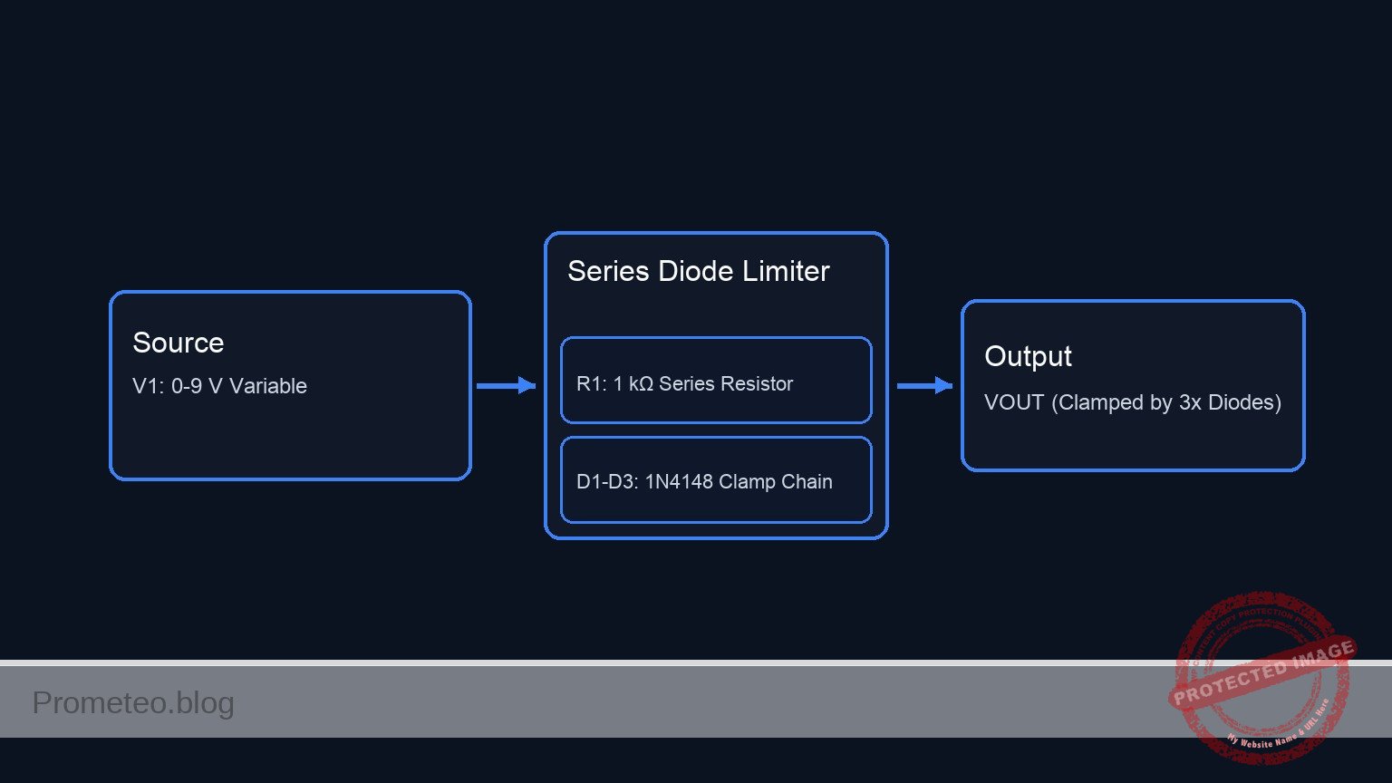
Follow me: