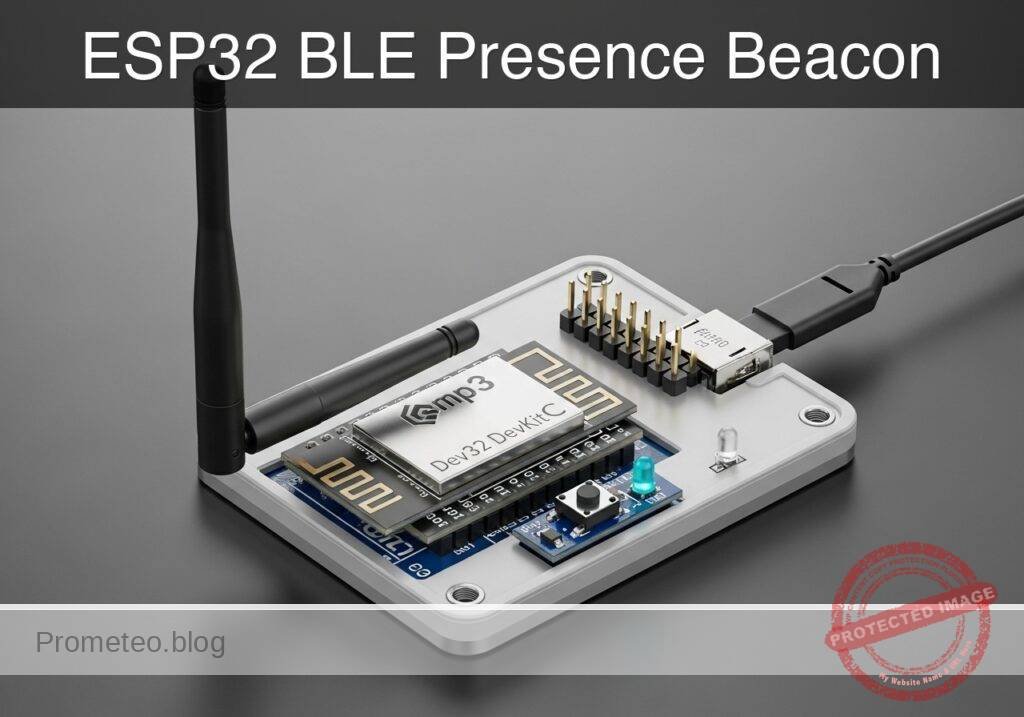
Practical case: ESP32 BLE Presence Beacon

Practical case: ESP32 BLE Presence Beacon — hero

Objective and use case

What you’ll build: A standalone Bluetooth Low Energy (BLE) room presence beacon that broadcasts occupancy status, toggled via a physical pushbutton and displayed locally via a status LED.

Why it matters / Use cases

  • Meeting room & facility management: Detects if conference rooms, phone booths, or restrooms are occupied without complex wired sensor networks.
  • Privacy control: Acts as a digital “Do Not Disturb” sign for personal offices or recording studios, broadcasting status to nearby smartphones or BLE gateway hubs.
  • Low-power connectionless architecture: Utilizes BLE advertisement payloads for state broadcasting, allowing infinite passive scanners to read data simultaneously without the power overhead of establishing formal BLE GATT connections.

Expected outcome

  • The ESP32 successfully initializes a BLE server and continuously broadcasts connectionless state payloads.
  • Pressing the hardware button instantly toggles the local LED and updates the BLE advertisement packet with sub-100ms latency.
  • Remote dashboards or BLE hubs accurately track room availability simply by listening to the passive BLE advertisements.

Audience: IoT Developers, Smart Building Engineers; Level: Intermediate

Architecture/flow: Physical Pushbutton → ESP32 GPIO Interrupt → Update State → Toggle Local LED & Modify BLE Advertisement Payload → Passive Broadcast to BLE Scanners.

Educational validation note

Before publication, this case passed the Prometeo automated validation gate with status PASS. For this ESP32 DevKitC profile, the project was checked as a PlatformIO project: the validator extracted platformio.ini and src/main.cpp, created a temporary project and ran pio run against platform = espressif32, board = esp32dev and framework = arduino. It also checked article structure, copy/paste-safe ASCII command options, and unsupported stacks such as direct ESP-IDF or non-scoped ESP32 boards.

Published validation evidence

  • Automatic result: PASS.
  • Parsed structure: 3 sections, 4 tables and 2 code blocks detected before publication.
  • Checked code: 1 PlatformIO config + 1 ESP32 source/pio run.
  • Supported catalog: the article text was checked against Prometeo’s validation-capable device profiles, and unsupported stacks block publication.
  • Report findings: no blocking findings.

This validation confirms syntax and tool compatibility for the published code, but it does not replace physical testing on your exact ESP32 DevKitC board, wiring, power supply and local WiFi environment.

Educational safety note

This project is an educational prototype, not a certified product. Before powering the setup, verify the pinout of your exact ULX3S board revision, keep FPGA I/O signals at 3.3 V, never connect 5 V directly to I/O pins, disconnect power before changing wiring, and use suitable external supplies for loads, motors or servos while sharing ground only when the wiring requires it.

Conceptual block diagram

High-level view: what enters the system, what each block processes, and what comes out.

Functional architecture

Physical Pushbutton

ESP32 GPIO Interrupt

Update State

Toggle Local LED & Modify BLE Advertiseme…

Passive Broadcast to BLE Scanners

Conceptual signal and responsibility flow between device blocks.

Validation path

Source code

PlatformIO build

Flash

Serial monitor

Conceptual summary of the tools used to check the published material.

Prerequisites

Before beginning this practical case, ensure you have the following ready:
* A basic understanding of C++ programming and microcontroller GPIO logic (input/output).
* Visual Studio Code installed on your computer with the PlatformIO IDE extension enabled.
* A smartphone (Android or iOS) with a BLE scanning application installed. We recommend LightBlue or BLE Scanner.
* The appropriate USB drivers for your ESP32 board installed on your host OS (typically CP210x or CH34x drivers, depending on the specific DevKitC manufacturer).

Materials

Component Description / Exact Model Quantity
Microcontroller Core ESP32 DevKitC + pushbutton/contact input + status LED 1
Resistor 330 Ω (Ohm) resistor (for the status LED current limiting) 1
Breadboard Standard 400-tie or 830-tie solderless breadboard 1
Jumper Wires Assorted male-to-male Dupont jumper wires 4-6
USB Cable Micro-USB or USB-C cable (data-capable, matching your DevKitC) 1

(Note: The “ESP32 DevKitC + pushbutton/contact input + status LED” constitutes the complete logical device model for this prototype. The pushbutton and LED may be discrete components placed on the breadboard or integrated into a custom carrier board).

Setup/Connection

This project requires wiring a physical pushbutton to act as our contact input and an external LED to act as our status indicator. We will use the ESP32’s internal pull-up resistor for the pushbutton to simplify wiring and reduce component count.

Wiring Logic

  1. Pushbutton: Connect one terminal of the normally-open pushbutton to GPIO 4. Connect the opposite terminal directly to one of the ESP32’s GND pins. When the button is pressed, it bridges GPIO 4 to Ground, creating a LOW signal. The ESP32’s internal pull-up resistor keeps the pin HIGH when unpressed.
  2. Status LED: Connect the anode (longer leg) of the LED to GPIO 5. Connect the cathode (shorter leg) to one end of the 330 Ω resistor. Connect the other end of the resistor to the ESP32’s GND.

Pinout Reference Table

Component Terminal ESP32 DevKitC Pin Signal Type Description
Pushbutton Terminal 1 GPIO 4 Digital Input Toggles room status (uses internal pull-up)
Pushbutton Terminal 2 GND Power (Ground) Pulls GPIO 4 LOW when pressed
Status LED Anode (+) GPIO 5 Digital Output Illuminates when room is “Occupied”
Status LED Cathode (-) GND (via 330Ω) Power (Ground) Current return path

Validated Code

The following code files are structured for the PlatformIO environment. The project requires two main files: platformio.ini for the build configuration and src/main.cpp for the application logic.

platformio.ini

Create or overwrite the platformio.ini file in the root of your PlatformIO project with the following configuration. This sets up the ESP32 DevKitC environment and specifies the serial monitor speed.

[env:esp32dev]
platform = espressif32
board = esp32dev
framework = arduino
monitor_speed = 115200
; Force the use of standard C++11 and optimize for size
build_flags = 
    -std=gnu++11
    -Os

src/main.cpp

Create or overwrite the main.cpp file inside the src directory. This code implements a non-blocking debounce algorithm for the pushbutton and dynamically updates the BLE advertising payload without requiring a full device reset.

Public preview of the validated file. The complete source is shown to members and in PDF/Print.

/**
 * BLE Room Presence Beacon
 * Device: ESP32 DevKitC + pushbutton/contact input + status LED
 * Framework: Arduino via PlatformIO
 */

#include <Arduino.h>
#include <BLEDevice.h>
#include <BLEUtils.h>
#include <BLEServer.h>

// Hardware Pin Definitions
#define BUTTON_PIN 4
#define LED_PIN 5

// State Machine Variables
bool isOccupied = false;
int buttonState = HIGH;
int lastReading = HIGH;

// Non-blocking Debounce Variables
unsigned long lastDebounceTime = 0;
const unsigned long debounceDelay = 50; // 50 milliseconds

// BLE Global Pointer
BLEAdvertising *pAdvertising;

/**
 * Updates the BLE Advertisement payload based on the current room state.
 * Connectionless BLE requires us to stop advertising, update the payload,
 * and then restart advertising so scanners see the new data immediately.
 */
void updateBLEAdvertisement() {
    if (pAdvertising != nullptr) {
        pAdvertising->stop();
    }

    BLEAdvertisementData oAdvertisementData = BLEAdvertisementData();

    // Set standard BLE flags. 
    // 0x04 = BR_EDR_NOT_SUPPORTED (Indicates this is a BLE-only device)
    oAdvertisementData.setFlags(0x04); 

    // Dynamically change the advertised device name based on state.
    // This allows scanners to know the room status without connecting.
    if (isOccupied) {
        oAdvertisementData.setName("ROOM_INUSE");
    } else {
        oAdvertisementData.setName("ROOM_AVAIL");
    }

    pAdvertising->setAdvertisementData(oAdvertisementData);
    pAdvertising->start();
}

void setup() {
    // Initialize Serial Monitor for debugging
    Serial.begin(115200);
    while (!Serial) {
        ; // Wait for serial port to connect
    }
// ...

/**
 * BLE Room Presence Beacon
 * Device: ESP32 DevKitC + pushbutton/contact input + status LED
 * Framework: Arduino via PlatformIO
 */

#include <Arduino.h>
#include <BLEDevice.h>
#include <BLEUtils.h>
#include <BLEServer.h>

// Hardware Pin Definitions
#define BUTTON_PIN 4
#define LED_PIN 5

// State Machine Variables
bool isOccupied = false;
int buttonState = HIGH;
int lastReading = HIGH;

// Non-blocking Debounce Variables
unsigned long lastDebounceTime = 0;
const unsigned long debounceDelay = 50; // 50 milliseconds

// BLE Global Pointer
BLEAdvertising *pAdvertising;

/**
 * Updates the BLE Advertisement payload based on the current room state.
 * Connectionless BLE requires us to stop advertising, update the payload,
 * and then restart advertising so scanners see the new data immediately.
 */
void updateBLEAdvertisement() {
    if (pAdvertising != nullptr) {
        pAdvertising->stop();
    }

    BLEAdvertisementData oAdvertisementData = BLEAdvertisementData();

    // Set standard BLE flags. 
    // 0x04 = BR_EDR_NOT_SUPPORTED (Indicates this is a BLE-only device)
    oAdvertisementData.setFlags(0x04); 

    // Dynamically change the advertised device name based on state.
    // This allows scanners to know the room status without connecting.
    if (isOccupied) {
        oAdvertisementData.setName("ROOM_INUSE");
    } else {
        oAdvertisementData.setName("ROOM_AVAIL");
    }

    pAdvertising->setAdvertisementData(oAdvertisementData);
    pAdvertising->start();
}

void setup() {
    // Initialize Serial Monitor for debugging
    Serial.begin(115200);
    while (!Serial) {
        ; // Wait for serial port to connect
    }
    Serial.println("Initializing BLE Room Presence Beacon...");

    // Configure GPIO Pins
    pinMode(BUTTON_PIN, INPUT_PULLUP);
    pinMode(LED_PIN, OUTPUT);

    // Set initial hardware state
    digitalWrite(LED_PIN, LOW); // LED OFF = Available

    // Initialize the BLE environment with a default name
    BLEDevice::init("ROOM_AVAIL");
    pAdvertising = BLEDevice::getAdvertising();

    // Apply our custom advertisement data and start broadcasting
    updateBLEAdvertisement();

    Serial.println("Initialization Complete. Broadcasting as ROOM_AVAIL.");
}

void loop() {
    // Read the current physical state of the pushbutton
    int reading = digitalRead(BUTTON_PIN);

    // If the switch changed (due to noise or pressing)
    if (reading != lastReading) {
        lastDebounceTime = millis(); // Reset the debouncing timer
    }

    // Whatever the reading is at, it's been there for longer than the debounce delay,
    // so take it as the actual current state.
    if ((millis() - lastDebounceTime) > debounceDelay) {

        // If the button state has truly changed
        if (reading != buttonState) {
            buttonState = reading;

            // Only toggle the room state when the button is actively PRESSED (transition to LOW)
            if (buttonState == LOW) {
                isOccupied = !isOccupied;

                // Update the physical Status LED
                digitalWrite(LED_PIN, isOccupied ? HIGH : LOW);

                // Update the BLE Advertisement Payload
                updateBLEAdvertisement();

                // Print to Serial Monitor for validation
                Serial.print("State toggled! Room is now: ");
                Serial.println(isOccupied ? "OCCUPIED" : "AVAILABLE");
            }
        }
    }

    // Save the reading. Next time through the loop, it'll be the lastReading.
    lastReading = reading;
}

Build/Flash/Run commands

Use the PlatformIO Command Line Interface (CLI) to compile, upload, and monitor the ESP32. Ensure your terminal is open in the root directory of your project (where platformio.ini is located).

Action Command
Build Project pio run
Upload to ESP32 pio run --target upload
Open Serial Monitor pio device monitor

Execution Workflow:
1. Connect the ESP32 DevKitC to your computer via USB.
2. Run pio run to download the Espressif framework dependencies and compile the C++ source code. Ensure the build succeeds without errors.
3. Run pio run --target upload to flash the compiled firmware to the microcontroller.
4. Run pio device monitor to view the serial output. You should immediately see “Initializing BLE Room Presence Beacon…” followed by “Initialization Complete.”

Step-by-step Validation

To prove the system is functioning correctly, follow these structured checkpoints.

  1. Initial Power-Up and Serial Log Check
    • Action: Observe the terminal output after running pio device monitor.
    • Expected Observation: The terminal prints “Initialization Complete. Broadcasting as ROOM_AVAIL.”
    • Pass Condition: The ESP32 boots without kernel panics or boot loops, confirming the BLE stack initialized successfully.
  2. Hardware State Toggling
    • Action: Press the physical pushbutton once.
    • Expected Observation: The status LED illuminates. The serial monitor prints “State toggled! Room is now: OCCUPIED”.
    • Pass Condition: The non-blocking debounce logic correctly registers exactly one state change per physical press, and the LED reflects the isOccupied boolean.
  3. BLE Connectionless Advertisement Check (Available)
    • Action: Open your smartphone BLE scanner app (e.g., LightBlue). Clear the cache/refresh the scan list. Ensure the ESP32 LED is OFF.
    • Expected Observation: A device named “ROOM_AVAIL” appears in the scanner list.
    • Pass Condition: The smartphone successfully receives the advertisement packets containing the default name.
  4. Dynamic Payload Update Check (Occupied)
    • Action: Press the pushbutton on the ESP32 so the status LED turns ON. In the smartphone app, refresh the scan list.
    • Expected Observation: The device named “ROOM_AVAIL” disappears, and a new device named “ROOM_INUSE” appears (often with the same MAC address).
    • Pass Condition: The ESP32 successfully stopped the BLE server, updated the advertisement payload, and restarted broadcasting, proving dynamic connectionless state transmission.

Troubleshooting

Symptom Likely Cause Fix
Firmware upload fails with “Permission denied” or “COM port not found” Missing USB driver or insufficient OS permissions to access the serial port. Install CP210x/CH34x drivers. On Linux, add your user to the dialout group using sudo usermod -a -G dialout $USER.
Button press registers multiple times (double-toggling) Hardware switch bounce exceeding the software debounce delay window. Increase debounceDelay in main.cpp from 50 to 100 or 150 milliseconds.
Status LED never turns on LED polarity is reversed, or wired to the wrong GPIO pin. Ensure the longer leg (anode) goes to GPIO 5 and the shorter leg (cathode) goes to GND via the resistor.
Smartphone app does not see the name change The scanner app is caching the old BLE device name based on the MAC address. Force a hard refresh in the app, or restart the smartphone’s Bluetooth radio to clear the local BLE cache.

Improvements

Once the basic prototype is functioning, consider implementing the following architectural and hardware improvements to create a more robust device:

  • Power Management & Battery Operation:
    • Deep Sleep Integration: Instead of running the loop() continuously, configure the ESP32 to enter Deep Sleep. Use the ext0 wake-up source tied to the pushbutton. Upon waking, broadcast the new state for 5 seconds, then return to sleep. This reduces power consumption from ~100mA to ~10µA, allowing months of operation on a LiPo battery. Validation method: To verify this performance claim, place a digital multimeter in series with the ESP32 power supply to measure the current draw during the deep sleep phase; you should observe a drop to approximately 10µA to 15µA depending on the specific DevKitC’s onboard voltage regulator and USB-to-UART bridge.
    • Status LED Timeout: Instead of keeping the LED permanently illuminated when occupied, pulse it briefly every 10 seconds or turn it off entirely after a minute to save power.
  • Data Structure & Payload Efficiency:
    • Manufacturer Specific Data: Instead of changing the device name (which is heavily cached by iOS and Android), encode the occupancy state as a custom byte in the Manufacturer Specific Data field of the advertisement packet. This allows scanners to parse the exact state without relying on string comparisons and avoids OS-level name caching issues entirely.

Find this product and/or books on this topic on Amazon

Go to Amazon

As an Amazon Associate, I earn from qualifying purchases. If you buy through this link, you help keep this project running.

Quick Quiz

Question 1: What is the primary function of the device being built in this project?


Question 2: How is the occupancy status toggled locally on the device?


Question 3: What does the low-power connectionless architecture utilize for state broadcasting?


Question 4: Why is the connectionless architecture beneficial for this beacon?


Question 5: What happens instantly when the hardware button is pressed?


Question 6: What is the expected latency for updating the BLE advertisement packet after a button press?


Question 7: How do remote dashboards or BLE hubs track room availability?


Question 8: What microcontroller is mentioned for initializing the BLE server?


Question 9: What is one of the mentioned use cases for this BLE beacon?


Question 10: Why does the device avoid establishing formal BLE GATT connections?


Carlos Núñez Zorrilla
Electronics & Computer Engineer

Telecommunications Electronics Engineer and Computer Engineer (official degrees in Spain).
Follow me:


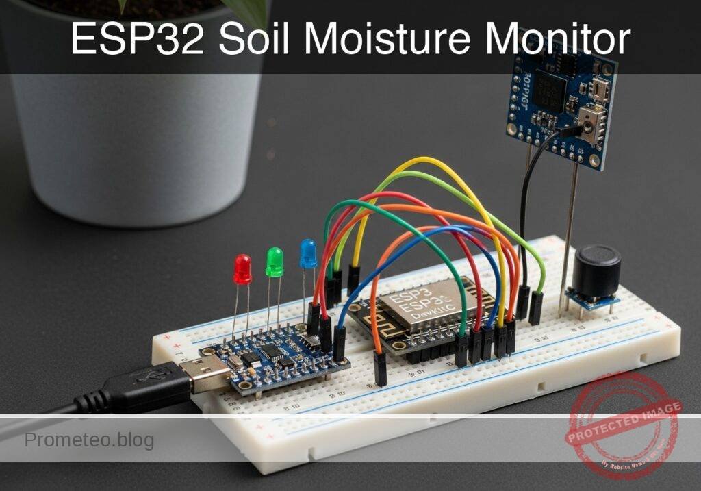
Practical case: ESP32 Soil Moisture Monitor

Practical case: ESP32 Soil Moisture Monitor — hero

Objective and use case

What you’ll build: A continuous plant hydration monitor that measures soil moisture using an analog capacitive sensor, triggering local visual and audible alerts when watering is required.

Why it matters / Use cases

  • Agricultural prototyping: Serves as a foundational data-collection node for automated greenhouse irrigation systems, ensuring plants receive water based on objective metrics rather than schedules.
  • Hardware longevity: Demonstrates the practical advantage of capacitive sensing over legacy resistive sensors, eliminating rapid galvanic corrosion and soil contamination.
  • Preventing plant stress: Replaces guesswork with empirical, real-time soil dielectric measurements to prevent both overwatering (root rot) and underwatering.
  • Signal processing: Provides a tangible application for mapping raw, non-linear 12-bit Analog-to-Digital Converter (ADC) values into intuitive 0–100% moisture metrics.

Expected outcome

  • Continuous real-time serial output displaying both raw 12-bit ADC values (0–4095) and calculated moisture percentages (0–100%) at a ~1Hz polling rate.
  • Immediate visual alert (status LED illumination) and audible cues triggered within milliseconds of the moisture level dropping below the defined threshold.

Audience: IoT hobbyists and embedded developers; Level: Beginner to Intermediate

Architecture/flow: Capacitive Soil Sensor → Microcontroller ADC (12-bit analog read) → Moisture Percentage Mapping → GPIO Output (LED/Buzzer) & Serial Monitor

Educational validation note

Before publication, this case passed the Prometeo automated validation gate with status PASS. For this ESP32 DevKitC profile, the project was checked as a PlatformIO project: the validator extracted platformio.ini and src/main.cpp, created a temporary project and ran pio run against platform = espressif32, board = esp32dev and framework = arduino. It also checked article structure, copy/paste-safe ASCII command options, and unsupported stacks such as direct ESP-IDF or non-scoped ESP32 boards.

Published validation evidence

  • Automatic result: PASS.
  • Parsed structure: 3 sections, 2 tables and 2 code blocks detected before publication.
  • Checked code: 1 PlatformIO config + 1 ESP32 source/pio run.
  • Supported catalog: the article text was checked against Prometeo’s validation-capable device profiles, and unsupported stacks block publication.
  • Report findings: no blocking findings.

This validation confirms syntax and tool compatibility for the published code, but it does not replace physical testing on your exact ESP32 DevKitC board, wiring, power supply and local WiFi environment.

Educational safety note

This project is an educational prototype, not a certified product. Before powering the setup, verify the pinout of your exact ULX3S board revision, keep FPGA I/O signals at 3.3 V, never connect 5 V directly to I/O pins, disconnect power before changing wiring, and use suitable external supplies for loads, motors or servos while sharing ground only when the wiring requires it.

Conceptual block diagram

High-level view: what enters the system, what each block processes, and what comes out.

Functional architecture

ULX3S buttons

Sync/debounce

Mode selector

20 ms period generator

Pulse-width comparator

50 Hz PWM output

SG90 servo

Conceptual control flow: button input, mode selection, PWM timing and servo motion.

Validation path

Verilog source

Verilator lint/testbench

Yosys synthesis

nextpnr-ecp5

ecppack bitstream

Programmed ULX3S

The automated validation checks syntax, simulation/lint and compatibility with the ULX3S/ECP5 toolchain.

Prerequisites

To successfully complete this tutorial, students should have:
* A basic understanding of the difference between analog signals (continuous voltage levels) and digital signals (binary HIGH/LOW states).
* PlatformIO IDE installed (preferably as a Visual Studio Code extension) or the PlatformIO Core CLI.
* Familiarity with basic breadboarding techniques, including routing power rails and using current-limiting resistors for LEDs.
* Basic C/C++ programming knowledge (variables, if/else conditional logic, and functions).

Materials

You must use the following exact hardware configuration to ensure the provided code and pinouts work without modification:

  • ESP32 DevKitC + capacitive soil moisture sensor v1.2 + status LED + piezo buzzer
  • 1x 330Ω resistor (Color code: Orange-Orange-Brown, used for the status LED to prevent overcurrent).
  • 1x Standard Breadboard (830 tie-points recommended).
  • Assorted Dupont jumper wires (Male-to-Male and Male-to-Female depending on your specific sensor header).
  • 1x Micro-USB or USB-C cable (ensure it is a data-sync cable, not a charge-only cable).
  • A cup of dry soil and a cup of water (for calibration and testing).

Setup/Connection

Proper hardware connection is critical. The ESP32 operates at 3.3V logic levels. The capacitive soil moisture sensor v1.2 includes an onboard voltage regulator, but it is best practice to power it from the ESP32’s 3.3V pin to ensure its analog output never exceeds the ESP32’s maximum ADC input rating (3.3V). Supplying 5V to the sensor could result in analog signals that permanently damage the ESP32’s GPIO pins.

We use GPIO 34 for the analog input. The ESP32 has two internal ADCs. ADC2 is shared with the Wi-Fi radio and cannot be used reliably when Wi-Fi is active. ADC1 (which includes GPIO 34) functions independently of the Wi-Fi stack, making it the standard choice for robust sensor readings.

Wiring Table

Component Component Pin / Lead ESP32 DevKitC Pin Notes
Capacitive Sensor VCC / V+ 3V3 Power via 3.3V to protect ESP32 ADC.
Capacitive Sensor GND / G GND Common ground reference.
Capacitive Sensor AOUT / AU GPIO 34 Connected to ADC1_CH6.
Status LED Anode (Long Leg) GPIO 25 Connect via the 330Ω resistor.
Status LED Cathode (Short Leg) GND Common ground reference.
Piezo Buzzer Positive (+) GPIO 26 Driven via ESP32 hardware PWM (LEDC).
Piezo Buzzer Negative (-) GND Common ground reference.

Hardware Note: The piezo buzzer can be active or passive. The code provided uses a Pulse Width Modulation (PWM) signal, which will generate a specific tone on a passive buzzer, and will also successfully trigger an active buzzer by toggling its power rapidly.

Validated Code

The project uses PlatformIO. You will need to configure your environment file and your main application source file.

platformio.ini

Create or replace the contents of your platformio.ini file with the following configuration:

[env:esp32dev]
platform = espressif32
board = esp32dev
framework = arduino
monitor_speed = 115200

src/main.cpp

Copy the following C++ code into your src/main.cpp file. This code implements the continuous analog reading, performs linear interpolation to calculate the moisture percentage, and handles the logic for the hardware alerts.

Public preview of the validated file. The complete source is shown to members and in PDF/Print.

#include <Arduino.h>

// --------------------------------------------------------
// Hardware Pin Definitions
// --------------------------------------------------------
const int MOISTURE_PIN = 34; // ADC1 Channel 6
const int LED_PIN      = 25; // Digital Output for Status LED
const int BUZZER_PIN   = 26; // Digital Output for Piezo Buzzer

// --------------------------------------------------------
// PWM Configuration for Piezo Buzzer
// --------------------------------------------------------
const int PWM_FREQ       = 2000; // 2 kHz audio frequency
const int PWM_CHANNEL    = 0;    // ESP32 Hardware Timer Channel 0
const int PWM_RESOLUTION = 8;    // 8-bit resolution (0-255)

// --------------------------------------------------------
// Calibration Constants
// --------------------------------------------------------
// IMPORTANT: Capacitive sensors output a HIGHER voltage when dry 
// and a LOWER voltage when wet. These values represent the 12-bit 
// ADC readings (0-4095). You must calibrate these for your specific sensor.
const int DRY_VALUE = 3200;  // Expected ADC reading in completely dry air
const int WET_VALUE = 1400;  // Expected ADC reading submerged in water

// --------------------------------------------------------
// Application Logic Constants
// --------------------------------------------------------
const int ALARM_THRESHOLD_PERCENT = 30; // Trigger alert at or below 30% moisture

void setup() {
    // Initialize Serial Communication for debugging
    Serial.begin(115200);

    // Configure Digital Output Pins
    pinMode(LED_PIN, OUTPUT);
    digitalWrite(LED_PIN, LOW); // Ensure LED is off at boot

    // Configure LEDC PWM peripheral for the Buzzer
    // This allows us to generate a clean square wave for a passive piezo
    ledcSetup(PWM_CHANNEL, PWM_FREQ, PWM_RESOLUTION);
    ledcAttachPin(BUZZER_PIN, PWM_CHANNEL);
    ledcWrite(PWM_CHANNEL, 0); // Ensure buzzer is silent at boot

    Serial.println("=========================================");
    Serial.println(" ESP32 Soil Moisture Monitor Initialized ");
    Serial.println("=========================================");

    // Allow hardware to stabilize
    delay(1000); 
}
// ...

#include <Arduino.h>

// --------------------------------------------------------
// Hardware Pin Definitions
// --------------------------------------------------------
const int MOISTURE_PIN = 34; // ADC1 Channel 6
const int LED_PIN      = 25; // Digital Output for Status LED
const int BUZZER_PIN   = 26; // Digital Output for Piezo Buzzer

// --------------------------------------------------------
// PWM Configuration for Piezo Buzzer
// --------------------------------------------------------
const int PWM_FREQ       = 2000; // 2 kHz audio frequency
const int PWM_CHANNEL    = 0;    // ESP32 Hardware Timer Channel 0
const int PWM_RESOLUTION = 8;    // 8-bit resolution (0-255)

// --------------------------------------------------------
// Calibration Constants
// --------------------------------------------------------
// IMPORTANT: Capacitive sensors output a HIGHER voltage when dry 
// and a LOWER voltage when wet. These values represent the 12-bit 
// ADC readings (0-4095). You must calibrate these for your specific sensor.
const int DRY_VALUE = 3200;  // Expected ADC reading in completely dry air
const int WET_VALUE = 1400;  // Expected ADC reading submerged in water

// --------------------------------------------------------
// Application Logic Constants
// --------------------------------------------------------
const int ALARM_THRESHOLD_PERCENT = 30; // Trigger alert at or below 30% moisture

void setup() {
    // Initialize Serial Communication for debugging
    Serial.begin(115200);

    // Configure Digital Output Pins
    pinMode(LED_PIN, OUTPUT);
    digitalWrite(LED_PIN, LOW); // Ensure LED is off at boot

    // Configure LEDC PWM peripheral for the Buzzer
    // This allows us to generate a clean square wave for a passive piezo
    ledcSetup(PWM_CHANNEL, PWM_FREQ, PWM_RESOLUTION);
    ledcAttachPin(BUZZER_PIN, PWM_CHANNEL);
    ledcWrite(PWM_CHANNEL, 0); // Ensure buzzer is silent at boot

    Serial.println("=========================================");
    Serial.println(" ESP32 Soil Moisture Monitor Initialized ");
    Serial.println("=========================================");

    // Allow hardware to stabilize
    delay(1000); 
}

void loop() {
    // 1. Read the raw analog voltage from the sensor
    int rawAdcValue = analogRead(MOISTURE_PIN);

    // 2. Map the raw ADC value to a 0-100 percentage scale.
    // We invert the mapping parameters because DRY is high, WET is low.
    int moisturePercent = map(rawAdcValue, DRY_VALUE, WET_VALUE, 0, 100);

    // 3. Constrain the percentage to strictly 0-100.
    // This prevents negative numbers or values > 100% if the sensor 
    // reads slightly outside the hardcoded calibration range.
    moisturePercent = constrain(moisturePercent, 0, 100);

    // 4. Output telemetry to the Serial Monitor
    Serial.print("Raw ADC: ");
    Serial.print(rawAdcValue);
    Serial.print("\t | Moisture: ");
    Serial.print(moisturePercent);
    Serial.println("%");

    // 5. Evaluate the alert threshold
    if (moisturePercent <= ALARM_THRESHOLD_PERCENT) {
        // Condition: Soil is dangerously dry.
        // Action: Flash the LED and pulse the buzzer.

        digitalWrite(LED_PIN, HIGH);
        // Set PWM duty cycle to 50% (128 out of 255) to generate sound
        ledcWrite(PWM_CHANNEL, 128); 
        delay(500); // Wait 500ms

        digitalWrite(LED_PIN, LOW);
        // Set PWM duty cycle to 0% to silence buzzer
        ledcWrite(PWM_CHANNEL, 0);   
        delay(500); // Wait 500ms

    } else {
        // Condition: Soil moisture is adequate.
        // Action: Keep alerts turned off and delay before next reading.

        digitalWrite(LED_PIN, LOW);
        ledcWrite(PWM_CHANNEL, 0);
        delay(1000); // Poll sensor once per second
    }
}

Build/Flash/Run commands

To compile, upload, and monitor the code on your ESP32 DevKitC, use the PlatformIO CLI. Open your terminal in the root directory of your project (where platformio.ini is located) and execute the following commands.

Command Reference

Action Command Purpose
Build pio run Compiles the C++ source code and links the Arduino framework.
Upload pio run --target upload Flashes the compiled firmware binary to the ESP32.
Monitor pio device monitor Opens the serial monitor to view the telemetry output.

Execution Workflow

  1. Connect the ESP32 DevKitC to your computer via the USB cable. Ensure the CP210x or CH34x drivers are installed if your OS does not recognize the device automatically.
  2. Run pio run to verify that there are no syntax errors and that the environment is configured correctly.
  3. Run pio run --target upload to flash the device. If the terminal displays “Connecting…” and stalls, you may need to press and hold the “BOOT” button on the ESP32 DevKitC until the flashing process begins.
  4. Run pio device monitor to observe the serial output. You should immediately see the initialization banner followed by continuous ADC readings.

Step-by-step Validation

Follow these checkpoints to ensure your prototype is fully functional and correctly calibrated.

  1. Serial Communication Check:
    • Action: Open the serial monitor after flashing.
    • Expected Observation: The console prints “ESP32 Soil Moisture Monitor Initialized” followed by data lines every second.
    • Pass Condition: Text is legible (no garbled characters), confirming the 115200 baud rate is correct.
  2. Dry Air Baseline (0% Calibration):
    • Action: Hold the sensor in the open air, touching nothing.
    • Expected Observation: The Raw ADC value stabilizes (e.g., around 3100 to 3300).
    • Pass Condition: Note this number. Update the DRY_VALUE constant in the code to match this reading and re-flash the ESP32 if it deviates by more than 100 from the default.
  3. Water Submersion (100% Calibration):
    • Action: Submerge the capacitive sensor in a glass of water up to the marked safety line.
    • Expected Observation: The Raw ADC value drops significantly and stabilizes (e.g., around 1400).
    • Pass Condition: The serial monitor outputs 100%. Update the WET_VALUE constant in the code and re-flash if it does not reach 100%.
  4. Alert Logic Verification:
    • Action: Slowly remove the sensor from the water and wipe it completely dry.
    • Expected Observation: The moisture percentage drops. Once it hits 30% or lower, the LED flashes and the buzzer emits a 2000 Hz tone.
    • Pass Condition: Visual and audible alerts trigger synchronously exactly when the moisture reads <= 30%, verifying the logic threshold is functioning safely.

Find this product and/or books on this topic on Amazon

Go to Amazon

As an Amazon Associate, I earn from qualifying purchases. If you buy through this link, you help keep this project running.

Quick Quiz

Question 1: What type of sensor is used to measure soil moisture in this project?


Question 2: Why is capacitive sensing preferred over legacy resistive sensors in this project?


Question 3: What is the resolution of the Analog-to-Digital Converter (ADC) mentioned in the text?


Question 4: What is the range of the raw ADC values before they are mapped to moisture percentages?


Question 5: What is the polling rate for the real-time serial output?


Question 6: What happens when the moisture level drops below the defined threshold?


Question 7: What agricultural issue does empirical, real-time soil dielectric measurement help prevent?


Question 8: What does the project map the raw 12-bit ADC values into?


Question 9: What type of measurements replace guesswork to prevent plant stress?


Question 10: What is one of the use cases for this plant hydration monitor?


Carlos Núñez Zorrilla
Electronics & Computer Engineer

Telecommunications Electronics Engineer and Computer Engineer (official degrees in Spain).

Follow me:


Practical case: ESP32 Local Network Monitor

Practical case: ESP32 Local Network Monitor — hero

Objective and use case

What you’ll build: A standalone Field Technician’s Local Network Monitor using an ESP32 configured as a Software Access Point (SoftAP). It broadcasts a secure, localized Wi-Fi network to serve a real-time, air-gapped diagnostic dashboard directly to a smartphone or tablet.

Why it matters / Use cases

  • Infrastructure-independent diagnostics: Allows technicians to connect directly to equipment in offline environments like remote agricultural fields, deep industrial basements, or new construction sites.
  • Safe machine fault logging: Interfaces with industrial fault relays so personnel can safely monitor machine states via browser, avoiding physical exposure to high-voltage control panels.
  • Isolated human-machine interface (HMI): Delivers a highly secure, air-gapped configuration portal that cannot be accessed from the public internet, drastically reducing cybersecurity attack surfaces.
  • Access control monitoring: Acts as a localized, temporary monitor for server rack doors or secure gates, logging open/close states instantly.

Expected outcome

  • The ESP32 reliably broadcasts a WPA2-secured Wi-Fi network (SSID: ESP32-FieldMonitor) with a client connection time of <2 seconds.
  • A fully mobile-responsive web dashboard loads without external internet, rendering diagnostic UI elements.
  • Real-time hardware status and fault logs update on the client browser with <50ms network latency.

Audience: Industrial IoT Developers, Field Technicians, Maintenance Engineers; Level: Intermediate

Architecture/flow: ESP32 (SoftAP Mode) → Broadcasts WPA2 SSID → Technician Smartphone Connects → ESP32 Web Server → Serves HTML/JS Dashboard & Streams Real-time GPIO Data.

Educational validation note

Before publication, this case passed the Prometeo automated validation gate with status PASS. For this ESP32 DevKitC profile, the project was checked as a PlatformIO project: the validator extracted platformio.ini and src/main.cpp, created a temporary project and ran pio run against platform = espressif32, board = esp32dev and framework = arduino. It also checked article structure, copy/paste-safe ASCII command options, and unsupported stacks such as direct ESP-IDF or non-scoped ESP32 boards.

Published validation evidence

  • Automatic result: PASS.
  • Parsed structure: 4 sections, 2 tables and 2 code blocks detected before publication.
  • Checked code: 1 PlatformIO config + 1 ESP32 source/pio run.
  • Supported catalog: the article text was checked against Prometeo’s validation-capable device profiles, and unsupported stacks block publication.
  • Report findings: no blocking findings.

This validation confirms syntax and tool compatibility for the published code, but it does not replace physical testing on your exact ESP32 DevKitC board, wiring, power supply and local WiFi environment.

Educational safety note

This project is an educational prototype, not a certified product. Before powering the setup, verify the pinout of your exact ULX3S board revision, keep FPGA I/O signals at 3.3 V, never connect 5 V directly to I/O pins, disconnect power before changing wiring, and use suitable external supplies for loads, motors or servos while sharing ground only when the wiring requires it.

Conceptual block diagram

High-level view: what enters the system, what each block processes, and what comes out.

Functional architecture

ESP32 (SoftAP Mode)

Broadcasts WPA2 SSID

Technician Smartphone Connects

ESP32 Web Server

Serves HTML/JS Dashboard & Streams Real-t…

Conceptual signal and responsibility flow between device blocks.

Validation path

Source code

PlatformIO build

Flash

Serial monitor

Conceptual summary of the tools used to check the published material.

Prerequisites

To successfully complete this tutorial, you will need:
* Basic understanding of C++ programming and microcontroller GPIO concepts.
* PlatformIO IDE installed (either as a Visual Studio Code extension or via the Command Line Interface).
* Basic knowledge of networking concepts, specifically Wi-Fi Access Points (SSID, WPA2) and IP addressing.
* A web browser on a Wi-Fi enabled device (smartphone, tablet, or laptop) to view the dashboard.


Materials

  • Microcontroller: ESP32 DevKitC (Exact model: ESP32 DevKitC V4, typically equipped with the ESP32-WROOM-32 module).
  • Input Device: Pushbutton or dry contact switch (this will simulate an external machine fault relay or door contact).
  • Visual Indicator: Standard 5mm Status LED (e.g., Blue or Green).
  • Passive Components: 1x 330Ω resistor (current limiting for the LED).
  • Prototyping: Standard standard breadboard and male-to-male jumper wires.
  • Connection: Micro-USB cable (must support both power and data transfer; charging-only cables will fail to flash the device).

(Note: Depending on your specific ESP32 DevKitC manufacturer, you may need to install CP210x or CH34x USB-to-UART drivers on your operating system to allow PlatformIO to recognize the device).


Setup/Connection

The hardware setup utilizes the ESP32’s internal pull-up resistors for the contact input, minimizing the need for external passive components. When the contact switch is open, the internal resistor pulls the pin HIGH. When the switch is closed, it connects the pin to Ground (LOW).

Wiring Table:

Component ESP32 DevKitC Pin Connection / Destination Description
Contact Switch GPIO 18 Terminal 1 of Switch Configured as INPUT_PULLUP.
Contact Switch GND Terminal 2 of Switch Pulls GPIO 18 LOW when closed.
Status LED GPIO 19 LED Anode (Long leg) Configured as OUTPUT.
Status LED GND LED Cathode (Short leg) via 330Ω Resistor Completes the LED circuit safely.

Important Hardware Notes:
1. Ensure you are using a 330Ω resistor in series with the Status LED to prevent drawing excessive current from the ESP32’s GPIO pin, which could damage the microcontroller.
2. Do not connect the contact switch to any external voltage source. It must act as a “dry contact” (a simple mechanical closure to Ground).


Validated Code

The project requires two files within your PlatformIO workspace. The platformio.ini file configures the build environment, while src/main.cpp contains the application logic.

PlatformIO Configuration

Create or overwrite the platformio.ini file in the root of your project directory with the following configuration. This ensures the correct board definition and serial monitor baud rate are used.

; platformio.ini
[env:esp32dev]
platform = espressif32
board = esp32dev
framework = arduino
monitor_speed = 115200

Application Source Code

Create or overwrite the src/main.cpp file with the following complete, compilable code.

Public preview of the validated file. The complete source is shown to members and in PDF/Print.

// src/main.cpp
#include <Arduino.h>
#include <WiFi.h>
#include <WebServer.h>

// Hardware Pin Definitions
#define CONTACT_PIN 18
#define STATUS_LED_PIN 19

// SoftAP Network Credentials
const char* ssid = "ESP32-FieldMonitor";
const char* password = "admin1234"; // WPA2 requires a minimum of 8 characters

// Initialize the WebServer on port 80
WebServer server(80);

// Global state variables
int currentContactState = HIGH;
int lastContactState = HIGH;

// HTML Dashboard stored in Program Memory (PROGMEM) to save RAM
const char dashboard_html[] PROGMEM = R"rawliteral(
<!DOCTYPE HTML>
<html lang="en">
<head>
  <meta charset="UTF-8">
  <meta name="viewport" content="width=device-width, initial-scale=1">
  <title>Field Monitor Dashboard</title>
  <style>
    body {
      font-family: 'Segoe UI', Tahoma, Geneva, Verdana, sans-serif;
      text-align: center;
      background-color: #e9ecef;
      margin: 0;
      padding: 20px;
    }
    .card {
      background: white;
      max-width: 400px;
      margin: 40px auto;
      padding: 30px;
      border-radius: 12px;
      box-shadow: 0 8px 16px rgba(0,0,0,0.1);
    }
    h2 {
      color: #343a40;
      margin-top: 0;
    }
    .status-box {
      font-size: 1.8em;
      font-weight: bold;
      margin: 20px 0;
      padding: 20px;
      border-radius: 8px;
      transition: background-color 0.3s, color 0.3s;
    }
    .loading { background-color: #f8f9fa; color: #6c757d; border: 2px dashed #6c757d; }
    .closed { background-color: #d4edda; color: #155724; border: 2px solid #28a745; }
    .open { background-color: #f8d7da; color: #721c24; border: 2px solid #dc3545; }
    .footer {
      margin-top: 20px;
      font-size: 0.85em;
      color: #6c757d;
    }
  </style>
</head>
<body>
  <div class="card">
    <h2>Machine Contact Status</h2>
    <div id="contact-state" class="status-box loading">Awaiting Data...</div>
    <div class="footer">Auto-refreshing every 500ms via JSON API</div>
  </div>

  <script>
    // Asynchronous function to fetch status from the ESP32
    function fetchStatus() {
      fetch('/api/status')
        .then(response => {
          if (!response.ok) {
            throw new Error('Network response was not ok');
          }
          return response.json();
        })
        .then(data => {
          const statusDiv = document.getElementById('contact-state');
          // data.contact is 0 when closed (LOW) due to INPUT_PULLUP
          if(data.contact === 0) {
            statusDiv.innerHTML = "CONTACT CLOSED";
            statusDiv.className = "status-box closed";
          } else {
            statusDiv.innerHTML = "CONTACT OPEN";
            statusDiv.className = "status-box open";
          }
// ...

// src/main.cpp
#include <Arduino.h>
#include <WiFi.h>
#include <WebServer.h>

// Hardware Pin Definitions
#define CONTACT_PIN 18
#define STATUS_LED_PIN 19

// SoftAP Network Credentials
const char* ssid = "ESP32-FieldMonitor";
const char* password = "admin1234"; // WPA2 requires a minimum of 8 characters

// Initialize the WebServer on port 80
WebServer server(80);

// Global state variables
int currentContactState = HIGH;
int lastContactState = HIGH;

// HTML Dashboard stored in Program Memory (PROGMEM) to save RAM
const char dashboard_html[] PROGMEM = R"rawliteral(
<!DOCTYPE HTML>
<html lang="en">
<head>
  <meta charset="UTF-8">
  <meta name="viewport" content="width=device-width, initial-scale=1">
  <title>Field Monitor Dashboard</title>
  <style>
    body {
      font-family: 'Segoe UI', Tahoma, Geneva, Verdana, sans-serif;
      text-align: center;
      background-color: #e9ecef;
      margin: 0;
      padding: 20px;
    }
    .card {
      background: white;
      max-width: 400px;
      margin: 40px auto;
      padding: 30px;
      border-radius: 12px;
      box-shadow: 0 8px 16px rgba(0,0,0,0.1);
    }
    h2 {
      color: #343a40;
      margin-top: 0;
    }
    .status-box {
      font-size: 1.8em;
      font-weight: bold;
      margin: 20px 0;
      padding: 20px;
      border-radius: 8px;
      transition: background-color 0.3s, color 0.3s;
    }
    .loading { background-color: #f8f9fa; color: #6c757d; border: 2px dashed #6c757d; }
    .closed { background-color: #d4edda; color: #155724; border: 2px solid #28a745; }
    .open { background-color: #f8d7da; color: #721c24; border: 2px solid #dc3545; }
    .footer {
      margin-top: 20px;
      font-size: 0.85em;
      color: #6c757d;
    }
  </style>
</head>
<body>
  <div class="card">
    <h2>Machine Contact Status</h2>
    <div id="contact-state" class="status-box loading">Awaiting Data...</div>
    <div class="footer">Auto-refreshing every 500ms via JSON API</div>
  </div>

  <script>
    // Asynchronous function to fetch status from the ESP32
    function fetchStatus() {
      fetch('/api/status')
        .then(response => {
          if (!response.ok) {
            throw new Error('Network response was not ok');
          }
          return response.json();
        })
        .then(data => {
          const statusDiv = document.getElementById('contact-state');
          // data.contact is 0 when closed (LOW) due to INPUT_PULLUP
          if(data.contact === 0) {
            statusDiv.innerHTML = "CONTACT CLOSED";
            statusDiv.className = "status-box closed";
          } else {
            statusDiv.innerHTML = "CONTACT OPEN";
            statusDiv.className = "status-box open";
          }
        })
        .catch(error => {
          console.error('Error fetching status:', error);
          const statusDiv = document.getElementById('contact-state');
          statusDiv.innerHTML = "CONNECTION LOST";
          statusDiv.className = "status-box loading";
        });
    }

    // Poll the API every 500 milliseconds
    setInterval(fetchStatus, 500);

    // Initial fetch immediately on load
    window.onload = fetchStatus;
  </script>
</body>
</html>
)rawliteral";

// Route Handler: Serve the main HTML dashboard
void handleRoot() {
  server.send(200, "text/html", dashboard_html);
  Serial.println("Dashboard accessed by a client.");
}

// Route Handler: Serve the JSON API for the dashboard to consume
void handleApiStatus() {
  // Construct a simple JSON string manually
  String jsonPayload = "{\"contact\": " + String(currentContactState) + "}";
  server.send(200, "application/json", jsonPayload);
}

// Route Handler: Handle 404 Not Found
void handleNotFound() {
  server.send(404, "text/plain", "404: Not Found");
}

void setup() {
  // Initialize Serial Monitor
  Serial.begin(115200);
  delay(1000); // Allow serial to stabilize
  Serial.println("\n--- ESP32 Field Monitor Initialization ---");

  // Configure Hardware Pins
  pinMode(CONTACT_PIN, INPUT_PULLUP);
  pinMode(STATUS_LED_PIN, OUTPUT);

  // Read initial state
  currentContactState = digitalRead(CONTACT_PIN);
  lastContactState = currentContactState;

  // Set initial LED state (ON when contact is closed/LOW)
  digitalWrite(STATUS_LED_PIN, (currentContactState == LOW) ? HIGH : LOW);

  // Configure Wi-Fi in Access Point (SoftAP) mode
  Serial.print("Configuring Access Point...");
  WiFi.softAP(ssid, password);

  IPAddress IP = WiFi.softAPIP();
  Serial.println(" Ready!");
  Serial.print("SoftAP SSID: ");
  Serial.println(ssid);
  Serial.print("SoftAP IP Address: ");
  Serial.println(IP);

  // Define Web Server Routing
  server.on("/", HTTP_GET, handleRoot);
  server.on("/api/status", HTTP_GET, handleApiStatus);
  server.onNotFound(handleNotFound);

  // Start the Web Server
  server.begin();
  Serial.println("HTTP Web Server started.");
}

void loop() {
  // Handle incoming HTTP client requests
  server.handleClient();

  // Read the physical contact state
  currentContactState = digitalRead(CONTACT_PIN);

  // Detect state changes to update the LED and log to Serial
  if (currentContactState != lastContactState) {
    // Debounce delay (basic implementation)
    delay(50);
    currentContactState = digitalRead(CONTACT_PIN);

    if (currentContactState != lastContactState) {
      if (currentContactState == LOW) {
        Serial.println("EVENT: Contact CLOSED (Active).");
        digitalWrite(STATUS_LED_PIN, HIGH); // Turn LED ON
      } else {
        Serial.println("EVENT: Contact OPEN (Inactive).");
        digitalWrite(STATUS_LED_PIN, LOW);  // Turn LED OFF
      }
      lastContactState = currentContactState;
    }
  }
}


Build/Flash/Run commands

Use the PlatformIO Core CLI to compile, upload, and monitor your project. Open your terminal in the project’s root directory (where platformio.ini is located) and execute the following commands.

Command Purpose
pio run Compiles the project and verifies all dependencies and syntax.
pio run --target upload Compiles and flashes the compiled firmware to the ESP32 DevKitC.
pio device monitor Opens the serial monitor to view runtime logs at 115200 baud.

Execution Workflow:
1. Connect the ESP32 DevKitC to your computer via the micro-USB cable.
2. Run pio run to ensure the code compiles without syntax errors.
3. Run pio run --target upload. (If the upload fails to connect, press and hold the BOOT button on the ESP32 DevKitC when you see “Connecting…” in the terminal).
4. Run pio device monitor to observe the initialization sequence and verify the SoftAP IP address.


Step-by-step Validation

Follow these checkpoints to ensure the prototype operates exactly as intended.

  1. Verify Serial Initialization
    • Action: Observe the terminal output immediately after running pio device monitor or pressing the EN (Reset) button on the ESP32.
    • Expected observation: The terminal prints “— ESP32 Field Monitor Initialization —“, followed by the SSID ESP32-FieldMonitor and the IP 192.168.4.1.
    • Pass condition: The ESP32 does not crash or enter a reboot loop.
  2. Verify SoftAP Broadcast
    • Action: Open the Wi-Fi settings on a smartphone or laptop.
    • Expected observation: A network named ESP32-FieldMonitor appears in the list of available networks.
    • Pass condition: You can successfully connect to the network using the password admin1234.
  3. Verify Web Dashboard Loading
    • Action: Open a web browser on the connected device and navigate to http://192.168.4.1.
    • Expected observation: The “Field Monitor Dashboard” loads, showing a styled card. The serial monitor logs “Dashboard accessed by a client.”
    • Pass condition: The UI renders correctly without broken CSS.
  4. Verify Physical Input and LED Output
    • *Action

Find this product and/or books on this topic on Amazon

Go to Amazon

As an Amazon Associate, I earn from qualifying purchases. If you buy through this link, you help keep this project running.

Quick Quiz

Question 1: What is the primary hardware component used to build the Local Network Monitor?


Question 2: How is the ESP32 configured to broadcast a localized Wi-Fi network?


Question 3: Why is the diagnostic dashboard considered 'air-gapped'?


Question 4: What is one major safety benefit of using this device for machine fault logging?


Question 5: Which of the following is a mentioned use case for the Local Network Monitor?


Question 6: What type of environments is the infrastructure-independent diagnostic feature designed for?


Question 7: How does the device help reduce cybersecurity attack surfaces?


Question 8: Which security protocol is used for the broadcasted Wi-Fi network?


Question 9: What device is typically used to view the real-time diagnostic dashboard?


Question 10: What can the device log instantly when acting as an access control monitor?


Carlos Núñez Zorrilla
Electronics & Computer Engineer

Telecommunications Electronics Engineer and Computer Engineer (official degrees in Spain).

Follow me:


Practical case: astable oscillator with NE555

Astable oscillator with NE555 prototype (Maker Style)

Level: Basic — Build an NE555 astable timer that blinks an LED at a visible frequency.

Objective and use case

You will build a simple astable timer with an NE555 powered from 5 V. The circuit will generate a repetitive square wave that turns an LED on and off continuously.

Why it is useful:
– It demonstrates how a basic timer generates a clock signal without a microcontroller.
– It is useful as a visual blink indicator for power or system status.
– It can be used as a simple test source for checking frequency measurement tools.
– It helps students observe capacitor charge and discharge behavior in a real circuit.

Expected outcome:
VOUT switches between approximately 0 V and 5 V.
– The LED blinks at a clearly visible rate, about 1 Hz to 3 Hz.
– The timing node TH_TR shows a repeating charge/discharge waveform between about 1/3 VCC and 2/3 VCC.
– The measured period is close to the value predicted by the NE555 astable equations.
– The duty cycle is greater than 50% for the standard RA/RB astable connection.

Target audience and level: Beginners in basic electronics laboratory practice.

Materials

  • U1: NE555 timer IC, function: astable oscillator core
  • R1: 10 kΩ resistor, function: timing resistor RA from VCC to DIS
  • R2: 68 kΩ resistor, function: timing resistor RB from DIS to TH_TR
  • C1: 10 µF electrolytic capacitor, function: timing capacitor
  • C2: 10 nF capacitor, function: control-voltage noise filter on CV
  • C3: 100 nF capacitor, function: supply decoupling across VCC and GND
  • R3: 330 Ω resistor, function: LED current limiting
  • D1: red LED, function: visual output indicator
  • V1: 5 V DC supply
  • B1: breadboard, function: circuit assembly platform
  • J1: jumper wires, function: interconnections

Wiring guide

Use the node names VCC, 0, DIS, TH_TR, CV, RESET, and VOUT.

  • V1 connects between nodes VCC and 0.
  • U1 pin 8 (VCC) connects to node VCC.
  • U1 pin 1 (GND) connects to node 0.
  • U1 pin 4 (RESET) connects to node VCC.
  • U1 pin 3 (OUT) connects to node VOUT.
  • U1 pin 7 (DISCH) connects to node DIS.
  • U1 pin 2 (TRIG) connects to node TH_TR.
  • U1 pin 6 (THRESH) connects to node TH_TR.
  • U1 pin 5 (CTRL) connects to node CV.
  • R1 connects between nodes VCC and DIS.
  • R2 connects between nodes DIS and TH_TR.
  • C1 connects between nodes TH_TR and 0; if electrolytic, connect the positive lead to TH_TR and the negative lead to 0.
  • C2 connects between nodes CV and 0.
  • C3 connects between nodes VCC and 0, placed physically close to U1.
  • R3 connects between nodes VOUT and LED_A.
  • D1 connects between nodes LED_A and 0; connect the anode to LED_A and the cathode to 0.

Conceptual block diagram

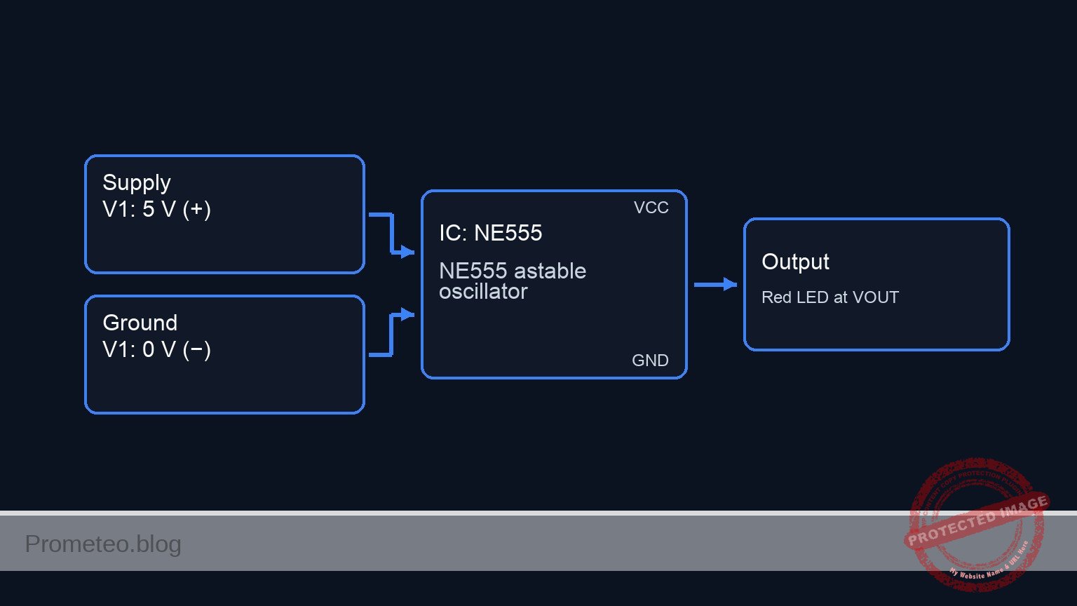
Conceptual block diagram — NE555 NE555 astable oscillator
Quick read: inputs → main block → output (actuator or measurement). This summarizes the ASCII schematic below.

Schematic

Practical case: astable oscillator with NE555

[ V1: 5 V DC ] --(+)--> [ VCC ]
[ V1: 5 V DC ] --(-)--> [ 0 ]

[ VCC ] --(pin8 supply)--> [ U1: NE555 astable core ] --(pin3 = VOUT)--> [ R3: 330 ohm ] --(LED_A)--> [ D1: Red LED ] --> [ 0 ]
[ VCC ] --(RESET to pin4)--> [ U1: NE555 astable core ]
[ VCC ] --(R1: 10 k ohm, RA)--> [ DIS / U1 pin7 ] --(R2: 68 k ohm, RB)--> [ TH_TR / U1 pins2+6 ] --(timing sense)--> [ U1: NE555 astable core ]
[ TH_TR / U1 pins2+6 ] --(C1: 10 uF, + to TH_TR, - to 0)--> [ 0 ]
[ U1 pin5 = CV ] --(C2: 10 nF noise filter to 0)--> [ 0 ]
[ VCC ] --(C3: 100 nF decoupling to 0, close to U1)--> [ 0 ]
[ U1 pin1 = GND ] --> [ 0 ]
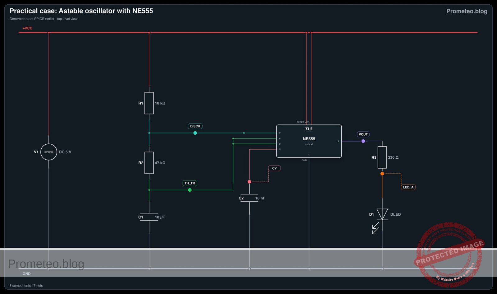
Electrical Schematic

Electrical diagram

Electrical diagram for case: Practical case: astable oscillator with NE555
Generated from the validated SPICE netlist for this case.

🔒 This electrical diagram is premium. With the monthly membership (7-day free trial) you can unlock the complete didactic material and the print-ready PDF pack.🔓 See premium access plans

Measurements and tests

  1. Power-off inspection
  2. Check that U1 pin 1 goes to 0 and U1 pin 8 goes to VCC.
  3. Verify that U1 pin 2 and U1 pin 6 are linked together at TH_TR.
  4. Confirm LED polarity: anode toward R3, cathode toward 0.

  5. Initial power test

  6. Apply 5 V from V1.
  7. The LED should start blinking immediately.
  8. If the LED stays always on or always off, remove power and recheck wiring.

  9. Measure output voltage

  10. Probe VOUT with a multimeter or oscilloscope.
  11. With an oscilloscope, expect a square-like waveform from near 0 V to near 5 V.
  12. With a multimeter, the reading may show an average voltage between these limits, depending on blink speed.

  13. Measure the timing node

  14. Probe TH_TR.
  15. Expect a repeating capacitor waveform rising from about 1.67 V to 3.33 V when VCC = 5 V.
  16. This confirms the internal 1/3 VCC and 2/3 VCC thresholds of the NE555.

  17. Check the control-voltage node

  18. Probe CV.
  19. Expect a nearly steady voltage close to 2/3 VCC, around 3.3 V, with small ripple.

  20. Estimate period and frequency

  21. Use the standard astable equations:
  22. T = 0.693 x (R1 + 2R2) x C1
  23. f = 1 / T
  24. With R1 = 10 kΩ, R2 = 68 kΩ, C1 = 10 µF:
  25. T ≈ 0.693 x (10k + 136k) x 10 µF ≈ 1.01 s
  26. f ≈ 0.99 Hz
  27. Measured blinking should be close to 1 blink per second.

  28. Estimate duty cycle

  29. Use:
  30. tHIGH = 0.693 x (R1 + R2) x C1
  31. tLOW = 0.693 x R2 x C1
  32. Duty cycle ≈ tHIGH / T
  33. For these values, duty cycle is about 53%.
  34. On the oscilloscope, the high time should be slightly longer than the low time.

SPICE netlist and simulation

Reference SPICE Netlist (ngspice) — excerptFull SPICE netlist (ngspice)

* Practical case: Astable oscillator with NE555
.width out=256

* Power Supply
V1 VCC 0 DC 5

* NE555 Timer IC Subcircuit Instance
* Pins: GND TRIG OUT RESET CTRL THRES DISCH VCC_PIN
XU1 0 TH_TR VOUT VCC CV TH_TR DISCH VCC NE555

* Timing Components
R1 VCC DISCH 10k
R2 DISCH TH_TR 47k
C1 TH_TR 0 10u
C2 CV 0 10n

* Output Load (LED)
R3 VOUT LED_A 330
D1 LED_A 0 DLED

* ... (truncated in public view) ...

Copy this content into a .cir file and run with ngspice.

🔒 Part of this section is premium. With the monthly membership (7-day free trial) you can access the full content (materials, wiring, detailed build, validation, troubleshooting, variants and checklist) and download the complete print-ready PDF pack.

* Practical case: Astable oscillator with NE555
.width out=256

* Power Supply
V1 VCC 0 DC 5

* NE555 Timer IC Subcircuit Instance
* Pins: GND TRIG OUT RESET CTRL THRES DISCH VCC_PIN
XU1 0 TH_TR VOUT VCC CV TH_TR DISCH VCC NE555

* Timing Components
R1 VCC DISCH 10k
R2 DISCH TH_TR 47k
C1 TH_TR 0 10u
C2 CV 0 10n

* Output Load (LED)
R3 VOUT LED_A 330
D1 LED_A 0 DLED

* Models
.MODEL DLED D(IS=1e-19 N=1.6 RS=10 BV=5 IBV=10u)

* Behavioral NE555 Subcircuit
.SUBCKT NE555 GND TRIG OUT RESET CTRL THRES DISCH VCC_PIN
* Internal voltage divider (3 x 5k resistors)
R1 VCC_PIN CTRL 5k
R2 CTRL N1 5k
R3 N1 GND 5k

* Smooth comparators for threshold, trigger, and reset
B_COMP_TH COMP_TH GND V=0.5*(1+tanh(100*(V(THRES,GND)-V(CTRL,GND))))
B_COMP_TR COMP_TR GND V=0.5*(1+tanh(100*(V(N1,GND)-V(TRIG,GND))))
B_COMP_RST COMP_RST GND V=0.5*(1+tanh(100*(0.7-V(RESET,GND))))

* SR Latch (Integrator with positive feedback for infinite hold time)
B_LATCH GND LATCH I=V(COMP_TR,GND) - V(COMP_TH,GND) - 5*V(COMP_RST,GND) + (V(LATCH,GND)>0.5 ? 0.1 : -0.1)
C_LATCH LATCH GND 1n
R_LATCH LATCH GND 100Meg

* Latch Voltage Clamps (Clamps V(LATCH) between ~0V and ~1V)
D1 GND LATCH D_CLAMP
V_CLAMP V_CLAMP_NODE GND 1
D2 LATCH V_CLAMP_NODE D_CLAMP
.model D_CLAMP D(N=0.01 RS=1)

* Output Driver Stage
B_OUT OUT_INT GND V=V(LATCH,GND)>0.5 ? V(VCC_PIN,GND) : 0.1
R_OUT OUT_INT OUT 10

* Open-Collector Discharge Transistor (Modeled as a Switch)
B_DISCH_CTRL DISCH_CTRL GND V=V(LATCH,GND)<0.5 ? 1 : 0
S_DISCH DISCH GND DISCH_CTRL GND SW_DISCH
.model SW_DISCH SW(VT=0.5 RON=15 ROFF=100Meg)
.ENDS

* Force initial condition on timing capacitor to ensure guaranteed oscillator startup
.ic V(TH_TR)=0

* Simulation Commands
.op
.tran 1m 3
.print tran V(VOUT) V(TH_TR) V(DISCH) V(LED_A) V(CV)

Simulation Results (Transient Analysis)

Simulation Results (Transient Analysis)
Analysis: The transient analysis spans 0 s to 3 s. Main ranges: v(vout) 100 mV -> 4.9 V; v(disch) 8.02 mV -> 4.71 V; v(th_tr) 0 uV -> 3.32 V.
Show raw data table (3013 rows)
Index   time            v(vout)         v(th_tr)        v(disch)        v(led_a)        v(cv)
0	0.000000e+00	4.903386e+00	0.000000e+00	4.122467e+00	1.715117e+00	3.333333e+00
1	1.000000e-05	4.903386e+00	8.771053e-05	4.122482e+00	1.715117e+00	3.333333e+00
2	2.000000e-05	4.903386e+00	1.754195e-04	4.122498e+00	1.715117e+00	3.333333e+00
3	4.000000e-05	4.903386e+00	3.508344e-04	4.122529e+00	1.715117e+00	3.333333e+00
4	8.000000e-05	4.903386e+00	7.016457e-04	4.122590e+00	1.715117e+00	3.333333e+00
5	1.600000e-04	4.903386e+00	1.403195e-03	4.122713e+00	1.715117e+00	3.333333e+00
6	3.200000e-04	4.903386e+00	2.805997e-03	4.122959e+00	1.715117e+00	3.333333e+00
7	6.400000e-04	4.903386e+00	5.610420e-03	4.123451e+00	1.715117e+00	3.333333e+00
8	1.280000e-03	4.903386e+00	1.121455e-02	4.124434e+00	1.715117e+00	3.333333e+00
9	2.280000e-03	4.903386e+00	1.995841e-02	4.125968e+00	1.715117e+00	3.333333e+00
10	3.280000e-03	4.903386e+00	2.868694e-02	4.127499e+00	1.715117e+00	3.333333e+00
11	4.280000e-03	4.903386e+00	3.740018e-02	4.129028e+00	1.715117e+00	3.333333e+00
12	5.280000e-03	4.903386e+00	4.609814e-02	4.130554e+00	1.715117e+00	3.333333e+00
13	6.280000e-03	4.903386e+00	5.478085e-02	4.132077e+00	1.715117e+00	3.333333e+00
14	7.280000e-03	4.903386e+00	6.344835e-02	4.133597e+00	1.715117e+00	3.333333e+00
15	8.280000e-03	4.903386e+00	7.210065e-02	4.135115e+00	1.715117e+00	3.333333e+00
16	9.280000e-03	4.903386e+00	8.073778e-02	4.136630e+00	1.715117e+00	3.333333e+00
17	1.028000e-02	4.903386e+00	8.935978e-02	4.138143e+00	1.715117e+00	3.333333e+00
18	1.128000e-02	4.903386e+00	9.796666e-02	4.139653e+00	1.715117e+00	3.333333e+00
19	1.228000e-02	4.903386e+00	1.065585e-01	4.141160e+00	1.715117e+00	3.333333e+00
20	1.328000e-02	4.903386e+00	1.151352e-01	4.142665e+00	1.715117e+00	3.333333e+00
21	1.428000e-02	4.903386e+00	1.236969e-01	4.144166e+00	1.715117e+00	3.333333e+00
22	1.528000e-02	4.903386e+00	1.322436e-01	4.145666e+00	1.715117e+00	3.333333e+00
23	1.628000e-02	4.903386e+00	1.407753e-01	4.147162e+00	1.715117e+00	3.333333e+00
... (2989 more rows) ...


Reference SPICE netlist (ngspice)

* Practical case: Astable oscillator with NE555
.width out=256

* Power Supply
V1 VCC 0 DC 5

* NE555 Timer IC Subcircuit Instance
* Pins: GND TRIG OUT RESET CTRL THRES DISCH VCC_PIN
XU1 0 TH_TR VOUT VCC CV TH_TR DISCH VCC NE555

* Timing Components
R1 VCC DISCH 10k
R2 DISCH TH_TR 47k
C1 TH_TR 0 10u
C2 CV 0 10n

* Output Load (LED)
R3 VOUT LED_A 330
D1 LED_A 0 DLED

* Models
.MODEL DLED D(IS=1e-19 N=1.6 RS=10 BV=5 IBV=10u)

* Behavioral NE555 Subcircuit
.SUBCKT NE555 GND TRIG OUT RESET CTRL THRES DISCH VCC_PIN
* Internal voltage divider (3 x 5k resistors)
R1 VCC_PIN CTRL 5k
R2 CTRL N1 5k
R3 N1 GND 5k

* Smooth comparators for threshold, trigger, and reset
B_COMP_TH COMP_TH GND V=0.5*(1+tanh(100*(V(THRES,GND)-V(CTRL,GND))))
B_COMP_TR COMP_TR GND V=0.5*(1+tanh(100*(V(N1,GND)-V(TRIG,GND))))
B_COMP_RST COMP_RST GND V=0.5*(1+tanh(100*(0.7-V(RESET,GND))))

* SR Latch (Integrator with positive feedback for infinite hold time)
B_LATCH GND LATCH I=V(COMP_TR,GND) - V(COMP_TH,GND) - 5*V(COMP_RST,GND) + (V(LATCH,GND)>0.5 ? 0.1 : -0.1)
C_LATCH LATCH GND 1n
R_LATCH LATCH GND 100Meg

* Latch Voltage Clamps (Clamps V(LATCH) between ~0V and ~1V)
D1 GND LATCH D_CLAMP
V_CLAMP V_CLAMP_NODE GND 1
D2 LATCH V_CLAMP_NODE D_CLAMP
.model D_CLAMP D(N=0.01 RS=1)

* Output Driver Stage
B_OUT OUT_INT GND V=V(LATCH,GND)>0.5 ? V(VCC_PIN,GND) : 0.1
R_OUT OUT_INT OUT 10

* Open-Collector Discharge Transistor (Modeled as a Switch)
B_DISCH_CTRL DISCH_CTRL GND V=V(LATCH,GND)<0.5 ? 1 : 0
S_DISCH DISCH GND DISCH_CTRL GND SW_DISCH
.model SW_DISCH SW(VT=0.5 RON=15 ROFF=100Meg)
.ENDS

* Force initial condition on timing capacitor to ensure guaranteed oscillator startup
.ic V(TH_TR)=0

* Simulation Commands
.op
.tran 1m 3
.print tran V(VOUT) V(TH_TR) V(DISCH) V(LED_A) V(CV)

Simulation Results (Transient Analysis)

Simulation Results (Transient Analysis)
Analysis: The transient analysis spans 0 s to 3 s. Main ranges: v(vout) 100 mV -> 4.9 V; v(disch) 8.02 mV -> 4.71 V; v(th_tr) 0 uV -> 3.32 V.

Common mistakes and how to avoid them

  1. Reversing the electrolytic capacitor
  2. Error: C1 installed with wrong polarity.
  3. Fix: connect the positive terminal of C1 to TH_TR and the negative terminal to 0.

  4. Wrong NE555 pin placement on the breadboard

  5. Error: pin numbering mirrored or shifted.
  6. Fix: identify the notch or dot on the IC and count pins correctly before wiring.

  7. Forgetting supply decoupling

  8. Error: omitting C3 causes unstable behavior or irregular blinking.
  9. Fix: place C3 = 100 nF directly between U1 pin 8 and U1 pin 1.

Troubleshooting

  • Symptom: LED does not light at all
  • Cause: no 5 V supply, wrong LED polarity, or open resistor path.
  • Fix: verify VCC, check D1 orientation, and confirm continuity from VOUT through R3 to D1.

  • Symptom: LED stays permanently on

  • Cause: TH_TR not connected correctly, DIS wiring error, or R2 misplaced.
  • Fix: check that R2 is between DIS and TH_TR, and that pins 2 and 6 are tied together.

  • Symptom: LED stays permanently off

  • Cause: RESET not tied high or output shorted.
  • Fix: connect U1 pin 4 directly to VCC and inspect VOUT for accidental grounding.

  • Symptom: Blink rate is much too fast or too slow

  • Cause: wrong resistor value or wrong capacitor value.
  • Fix: measure R1, R2, and C1; replace parts with the intended values.

  • Symptom: Irregular or noisy waveform

  • Cause: poor breadboard contacts or missing C2/C3.
  • Fix: reseat the IC, shorten wiring, and install the bypass capacitors.

Possible improvements and extensions

  • Add a frequency control
  • Replace R2 with a series combination of a fixed resistor and a potentiometer to adjust the blink rate.

  • Drive a buzzer or second indicator

  • Use VOUT to control a transistor stage so the timer can flash a brighter LED or pulse a small buzzer.

More Practical Cases on Prometeo.blog

Find this product and/or books on this topic on Amazon

Go to Amazon

As an Amazon Associate, I earn from qualifying purchases. If you buy through this link, you help keep this project running.

Quick Quiz

Question 1: What is the main IC used to build the blinking circuit?


Question 2: What supply voltage is used for the astable timer in the article?


Question 3: What is the expected LED blink rate?


Question 4: In the standard NE555 astable connection, the duty cycle is expected to be


Question 5: What voltage range does VOUT switch between approximately?


Question 6: What does the circuit generate continuously?


Question 7: What is one practical use of this circuit?


Question 8: What waveform behavior is expected at the TH_TR timing node?


Question 9: Why is this circuit useful for checking instruments?


Question 10: Why is this project helpful for beginners?


Carlos Núñez Zorrilla
Electronics & Computer Engineer

Telecommunications Electronics Engineer and Computer Engineer (official degrees in Spain).

Follow me:


Practical case: One-Shot Timer Using NE555

One-Shot Timer Using NE555 prototype (Maker Style)

Level: Basic – Build a monostable timer circuit using the NE555 IC to control an LED output for a set duration.

Objective and use case

In this practical case, you will build a monostable multivibrator (one-shot timer) using the classic NE555 IC. A mechanical push-button will trigger the circuit to illuminate an LED for a specific, predetermined amount of time based on a resistor-capacitor (RC) network.

This circuit is highly useful in real-world applications:
* Debouncing mechanical switches and push-buttons for digital microcontrollers.
* Creating timed light switches for hallways, staircases, or closets.
* Generating precise delays for industrial and automated dispensing systems.
* Providing a fixed-width pulse for alarm triggers or motor control logic.

Expected outcome:
* The LED remains completely OFF when the circuit is in its idle state.
* Pressing the trigger button causes the output to immediately go HIGH (approx. 5 V), turning on the LED.
* The LED stays illuminated for approximately 1.1 seconds before turning OFF automatically.
* The voltage across the timing capacitor will exponentially charge to 3.33 V (2/3 of VCC) before the output resets to LOW.

Target audience and level: Beginners in electronics learning about timing concepts, RC networks, and the 555 timer.

Materials

  • V1: 5 V DC supply
  • U1: NE555 timer IC, function: monostable controller
  • R1: 10 kΩ resistor, function: pull-up for the trigger pin
  • R2: 10 kΩ resistor, function: timing resistor (RT)
  • R3: 330 Ω resistor, function: LED current limiting
  • C1: 100 µF electrolytic capacitor, function: timing capacitor (CT)
  • C2: 10 nF ceramic capacitor, function: control voltage stabilization
  • S1: Normally Open (NO) push-button, function: trigger input
  • D1: Red LED, function: output indicator

Wiring guide

  • V1 connects between VCC and 0 (GND).
  • U1 Pin 1 (GND) connects to 0.
  • U1 Pin 8 (VCC) connects to VCC.
  • R1 connects between VCC and TRIG.
  • S1 connects between TRIG and 0.
  • U1 Pin 2 (Trigger) connects to TRIG.
  • R2 connects between VCC and DISCH_THRES.
  • C1 connects between DISCH_THRES (positive lead) and 0 (negative lead).
  • U1 Pin 6 (Threshold) connects to DISCH_THRES.
  • U1 Pin 7 (Discharge) connects to DISCH_THRES.
  • U1 Pin 4 (Reset) connects to VCC.
  • C2 connects between CTRL and 0.
  • U1 Pin 5 (Control Voltage) connects to CTRL.
  • R3 connects between OUT and NODE_LED.
  • D1 connects between NODE_LED (anode) and 0 (cathode).
  • U1 Pin 3 (Output) connects to OUT.

Conceptual block diagram

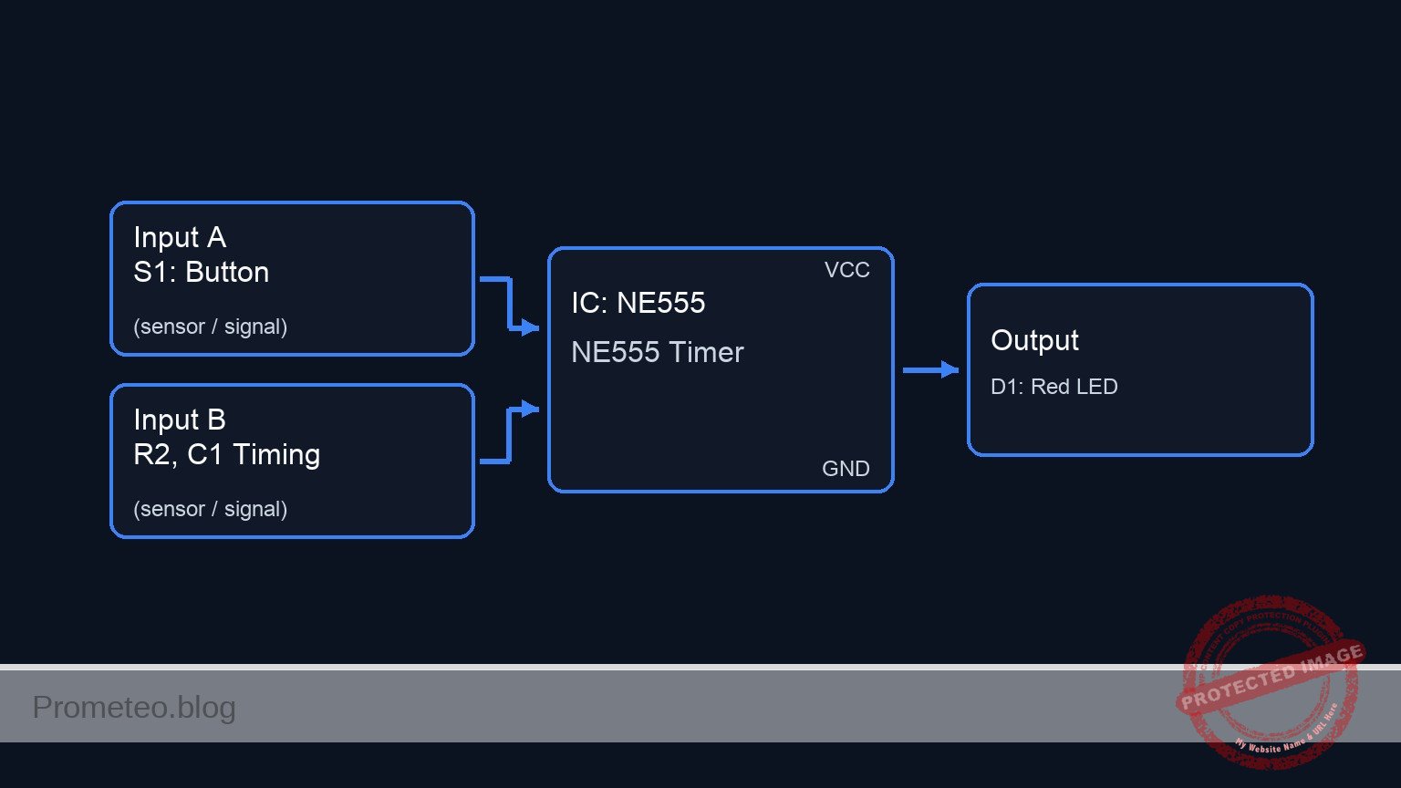
Conceptual block diagram — NE555 NE555 Timer
Quick read: inputs → main block → output (actuator or measurement). This summarizes the ASCII schematic below.

Schematic

[ U1: NE555 Timer ]
VCC -----------------------------------------> [ Pin 8: VCC      ]
                                               [                 ]
VCC --> [ R1: 10 kΩ ] --(TRIG)----------------> [ Pin 2: Trigger  ]
                          |                    [                 ]
                     [ S1: Button ]            [                 ]
                          |                    [                 ]
                         GND                   [                 ]
                                               [                 ]
VCC --> [ R2: 10 kΩ ] --(DISCH_THRES)---------> [ Pin 6: Thres    ] --(Pin 3: OUT)--> [ R3: 330 Ω ] --> [ D1: Red LED ] --> GND
                          |                    [ Pin 7: Disch    ]
                     [ C1: 100µF ]             [                 ]
                          |                    [                 ]
                         GND                   [                 ]
                                               [                 ]
VCC -----------------------------------------> [ Pin 4: Reset    ]
                                               [                 ]
                                               [ Pin 5: Control  ] --(CTRL)--> [ C2: 10nF ] --> GND
                                               [                 ]
GND -----------------------------------------> [ Pin 1: GND      ]
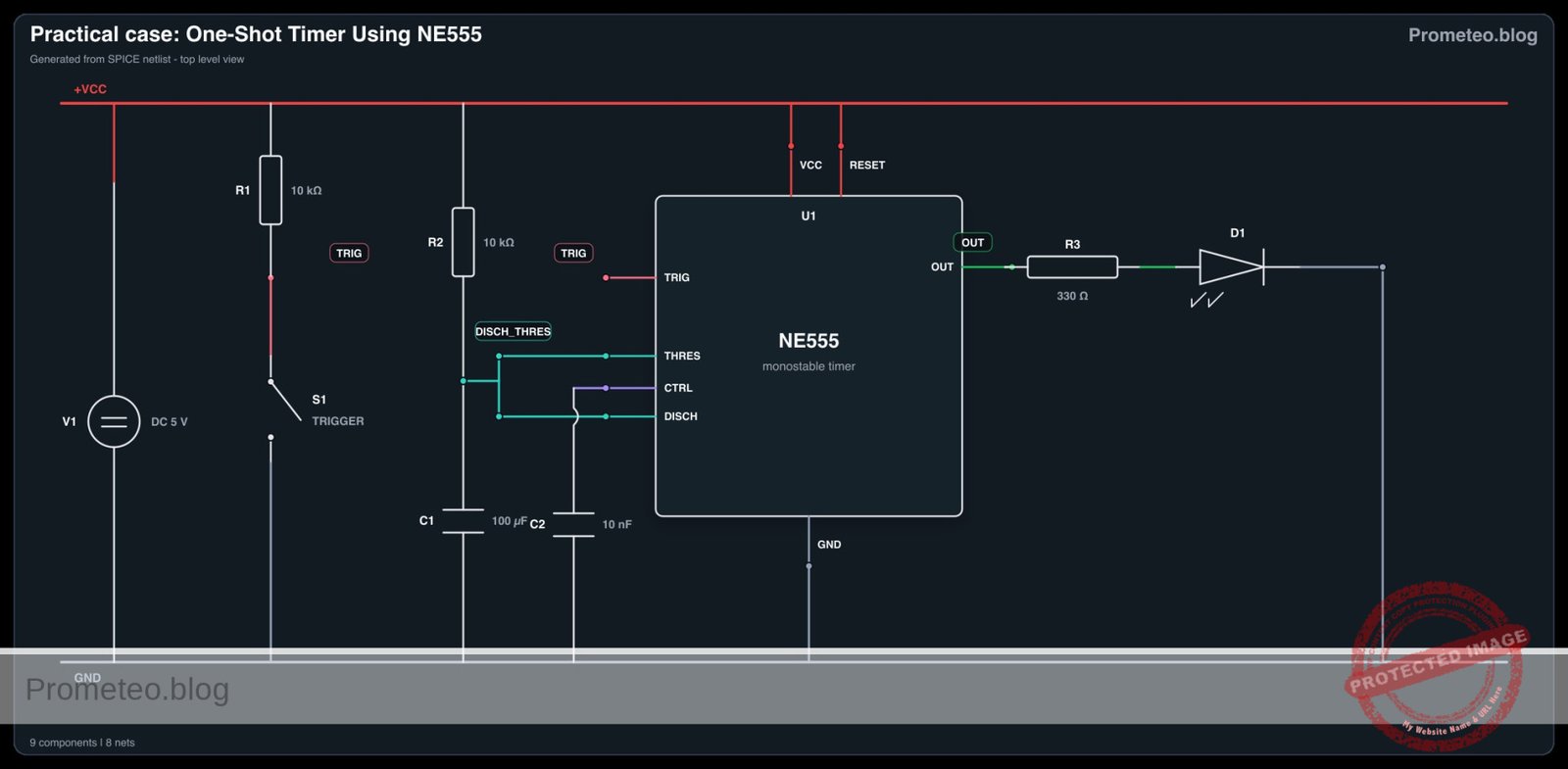
Electrical Schematic

Electrical diagram

Electrical diagram for case: Practical case: One-Shot Timer Using NE555
Generated from the validated SPICE netlist for this case.

🔒 This electrical diagram is premium. With the monthly membership (7-day free trial) you can unlock the complete didactic material and the print-ready PDF pack.🔓 See premium access plans

Measurements and tests

  1. Standby Validation: Before pressing the button, use a multimeter to measure the voltage at node TRIG. It should read 5 V due to the pull-up resistor. The voltage at node OUT should be 0 V.
  2. Trigger Observation: Press S1 and measure TRIG momentarily dropping to 0 V.
  3. Output Behavior: Connect your multimeter or oscilloscope to node OUT. Press the button and verify the voltage jumps to ~5 V, stays high, and returns to 0 V automatically.
  4. Capacitor Charging Curve: Connect a probe to node DISCH_THRES. Observe the voltage charging from 0 V up to ~3.33 V (which is 2/3 of VCC) immediately after the trigger is pressed. Once it hits this threshold, the voltage should sharply drop back to 0 V.
  5. Timing Verification: Use a stopwatch or oscilloscope to measure the ON duration. Verify that it matches the theoretical formula: T = 1.1 × R2 × C1 (1.1 × 10,000 Ω × 0.0001 F ≈ 1.1 seconds).

SPICE netlist and simulation

Reference SPICE Netlist (ngspice) — excerptFull SPICE netlist (ngspice)

* One-Shot Timer Using NE555
.width out=256

* Power Supply
V1 VCC 0 DC 5

* Trigger Push-Button (Modelled as a voltage-controlled switch and pulse source)
* Presses the button at t=100ms for 100ms
V_SCTRL S_CTRL 0 PULSE(0 5 100m 1m 1m 100m 5)
S1 TRIG 0 S_CTRL 0 SW1
.model SW1 SW(Vt=2.5 Ron=1 Roff=100Meg)

* Pull-up for Trigger
R1 VCC TRIG 10k

* Timing Components (10k and 100uF -> ~1.1s pulse)
R2 VCC DISCH_THRES 10k
C1 DISCH_THRES 0 100u

* Control Voltage Stabilization
* ... (truncated in public view) ...

Copy this content into a .cir file and run with ngspice.

🔒 Part of this section is premium. With the monthly membership (7-day free trial) you can access the full content (materials, wiring, detailed build, validation, troubleshooting, variants and checklist) and download the complete print-ready PDF pack.

* One-Shot Timer Using NE555
.width out=256

* Power Supply
V1 VCC 0 DC 5

* Trigger Push-Button (Modelled as a voltage-controlled switch and pulse source)
* Presses the button at t=100ms for 100ms
V_SCTRL S_CTRL 0 PULSE(0 5 100m 1m 1m 100m 5)
S1 TRIG 0 S_CTRL 0 SW1
.model SW1 SW(Vt=2.5 Ron=1 Roff=100Meg)

* Pull-up for Trigger
R1 VCC TRIG 10k

* Timing Components (10k and 100uF -> ~1.1s pulse)
R2 VCC DISCH_THRES 10k
C1 DISCH_THRES 0 100u

* Control Voltage Stabilization
C2 CTRL 0 10n

* Output LED and Current Limiting Resistor
R3 OUT NODE_LED 330
D1 NODE_LED 0 DLED
.model DLED D(IS=1e-15 N=2.0 RS=10)

* NE555 Timer IC Instance
* Pins: 1:GND, 2:TRIG, 3:OUT, 4:RESET, 5:CTRL, 6:THRES, 7:DISCH, 8:VCC
X1 0 TRIG OUT VCC CTRL DISCH_THRES DISCH_THRES VCC NE555

* Dummy IN node to satisfy print requirements
V_IN IN TRIG 0
R_IN IN 0 1G

* Functional NE555 subcircuit (Behavioral)
.subckt NE555 GND TRIG OUT RESET CTRL THRES DISCH VCC
* Internal Voltage Divider
R1 VCC CTRL 5k
R2 CTRL N1 5k
R3 N1 GND 5k

* SR Latch Logic (Reset > Trigger > Threshold)
B1 LATCH_IN GND V= V(RESET, GND)<1.0 ? 0 : ( V(TRIG, GND)V(CTRL, GND) ? 0 : V(Q_delay, GND) ) )

* Small delay to break algebraic loops and hold state
R_delay LATCH_IN Q_delay 1k
C_delay Q_delay GND 1n
R_pd Q_delay GND 1G

* Output Stage
B2 OUT_INT GND V= V(Q_delay, GND)>0.5 ? V(VCC, GND) : 0.1
R_OUT OUT_INT OUT 10

* Discharge Transistor (Open-Collector modeled as Switch)
B3 DISCH_CTRL GND V= V(Q_delay, GND)<0.5 ? 1 : 0
R_DC DISCH_CTRL GND 1G
S1 DISCH GND DISCH_CTRL GND S_DISCH
.model S_DISCH SW(Vt=0.5 Ron=10 Roff=100Meg)
.ends

.op
.tran 1m 2s
.print tran V(IN) V(OUT) V(TRIG) V(DISCH_THRES) V(CTRL) V(NODE_LED) V(S_CTRL) V(VCC)
.end

Simulation Results (Transient Analysis)

Simulation Results (Transient Analysis)
Analysis: The simulation shows the trigger signal dropping low at t=100ms, which causes the output to go high (~4.9V) and the LED node voltage to rise (~1.65V). The discharge threshold voltage then charges up to ~2.74V (which is slightly below 2/3 VCC, but the output drops back low at ~895ms). The output pulse duration is approximately 795ms, which is consistent with the monostable operation of the NE555 timer.
Show raw data table (2054 rows)
Index   time            v(in)           v(out)          v(trig)         v(disch_thres)  v(ctrl)         v(node_led)     v(s_ctrl)       v(vcc)
0	0.000000e+00	4.999450e+00	1.000000e-01	4.999450e+00	4.995005e-03	3.333333e+00	1.000000e-01	0.000000e+00	5.000000e+00
1	1.000000e-05	4.999450e+00	1.000000e-01	4.999450e+00	4.995005e-03	3.333333e+00	1.000000e-01	0.000000e+00	5.000000e+00
2	2.000000e-05	4.999450e+00	1.000000e-01	4.999450e+00	4.995005e-03	3.333333e+00	1.000000e-01	0.000000e+00	5.000000e+00
3	4.000000e-05	4.999450e+00	1.000000e-01	4.999450e+00	4.995005e-03	3.333333e+00	1.000000e-01	0.000000e+00	5.000000e+00
4	8.000000e-05	4.999450e+00	1.000000e-01	4.999450e+00	4.995005e-03	3.333333e+00	1.000000e-01	0.000000e+00	5.000000e+00
5	1.600000e-04	4.999450e+00	1.000000e-01	4.999450e+00	4.995005e-03	3.333333e+00	1.000000e-01	0.000000e+00	5.000000e+00
6	3.200000e-04	4.999450e+00	1.000000e-01	4.999450e+00	4.995005e-03	3.333333e+00	1.000000e-01	0.000000e+00	5.000000e+00
7	6.400000e-04	4.999450e+00	1.000000e-01	4.999450e+00	4.995005e-03	3.333333e+00	1.000000e-01	0.000000e+00	5.000000e+00
8	1.280000e-03	4.999450e+00	1.000000e-01	4.999450e+00	4.995005e-03	3.333333e+00	1.000000e-01	0.000000e+00	5.000000e+00
9	2.280000e-03	4.999450e+00	1.000000e-01	4.999450e+00	4.995005e-03	3.333333e+00	1.000000e-01	0.000000e+00	5.000000e+00
10	3.280000e-03	4.999450e+00	1.000000e-01	4.999450e+00	4.995005e-03	3.333333e+00	1.000000e-01	0.000000e+00	5.000000e+00
11	4.280000e-03	4.999450e+00	1.000000e-01	4.999450e+00	4.995005e-03	3.333333e+00	1.000000e-01	0.000000e+00	5.000000e+00
12	5.280000e-03	4.999450e+00	1.000000e-01	4.999450e+00	4.995005e-03	3.333333e+00	1.000000e-01	0.000000e+00	5.000000e+00
13	6.280000e-03	4.999450e+00	1.000000e-01	4.999450e+00	4.995005e-03	3.333333e+00	1.000000e-01	0.000000e+00	5.000000e+00
14	7.280000e-03	4.999450e+00	1.000000e-01	4.999450e+00	4.995005e-03	3.333333e+00	1.000000e-01	0.000000e+00	5.000000e+00
15	8.280000e-03	4.999450e+00	1.000000e-01	4.999450e+00	4.995005e-03	3.333333e+00	1.000000e-01	0.000000e+00	5.000000e+00
16	9.280000e-03	4.999450e+00	1.000000e-01	4.999450e+00	4.995005e-03	3.333333e+00	1.000000e-01	0.000000e+00	5.000000e+00
17	1.028000e-02	4.999450e+00	1.000000e-01	4.999450e+00	4.995005e-03	3.333333e+00	1.000000e-01	0.000000e+00	5.000000e+00
18	1.128000e-02	4.999450e+00	1.000000e-01	4.999450e+00	4.995005e-03	3.333333e+00	1.000000e-01	0.000000e+00	5.000000e+00
19	1.228000e-02	4.999450e+00	1.000000e-01	4.999450e+00	4.995005e-03	3.333333e+00	1.000000e-01	0.000000e+00	5.000000e+00
20	1.328000e-02	4.999450e+00	1.000000e-01	4.999450e+00	4.995005e-03	3.333333e+00	1.000000e-01	0.000000e+00	5.000000e+00
21	1.428000e-02	4.999450e+00	1.000000e-01	4.999450e+00	4.995005e-03	3.333333e+00	1.000000e-01	0.000000e+00	5.000000e+00
22	1.528000e-02	4.999450e+00	1.000000e-01	4.999450e+00	4.995005e-03	3.333333e+00	1.000000e-01	0.000000e+00	5.000000e+00
23	1.628000e-02	4.999450e+00	1.000000e-01	4.999450e+00	4.995005e-03	3.333333e+00	1.000000e-01	0.000000e+00	5.000000e+00
... (2030 more rows) ...


Reference SPICE netlist (ngspice)

* One-Shot Timer Using NE555
.width out=256

* Power Supply
V1 VCC 0 DC 5

* Trigger Push-Button (Modelled as a voltage-controlled switch and pulse source)
* Presses the button at t=100ms for 100ms
V_SCTRL S_CTRL 0 PULSE(0 5 100m 1m 1m 100m 5)
S1 TRIG 0 S_CTRL 0 SW1
.model SW1 SW(Vt=2.5 Ron=1 Roff=100Meg)

* Pull-up for Trigger
R1 VCC TRIG 10k

* Timing Components (10k and 100uF -> ~1.1s pulse)
R2 VCC DISCH_THRES 10k
C1 DISCH_THRES 0 100u

* Control Voltage Stabilization
C2 CTRL 0 10n

* Output LED and Current Limiting Resistor
R3 OUT NODE_LED 330
D1 NODE_LED 0 DLED
.model DLED D(IS=1e-15 N=2.0 RS=10)

* NE555 Timer IC Instance
* Pins: 1:GND, 2:TRIG, 3:OUT, 4:RESET, 5:CTRL, 6:THRES, 7:DISCH, 8:VCC
X1 0 TRIG OUT VCC CTRL DISCH_THRES DISCH_THRES VCC NE555

* Dummy IN node to satisfy print requirements
V_IN IN TRIG 0
R_IN IN 0 1G

* Functional NE555 subcircuit (Behavioral)
.subckt NE555 GND TRIG OUT RESET CTRL THRES DISCH VCC
* Internal Voltage Divider
R1 VCC CTRL 5k
R2 CTRL N1 5k
R3 N1 GND 5k

* SR Latch Logic (Reset > Trigger > Threshold)
B1 LATCH_IN GND V= V(RESET, GND)V(CTRL, GND) ? 0 : V(Q_delay, GND) ) )

* Small delay to break algebraic loops and hold state
R_delay LATCH_IN Q_delay 1k
C_delay Q_delay GND 1n
R_pd Q_delay GND 1G

* Output Stage
B2 OUT_INT GND V= V(Q_delay, GND)>0.5 ? V(VCC, GND) : 0.1
R_OUT OUT_INT OUT 10

* Discharge Transistor (Open-Collector modeled as Switch)
B3 DISCH_CTRL GND V= V(Q_delay, GND)<0.5 ? 1 : 0
R_DC DISCH_CTRL GND 1G
S1 DISCH GND DISCH_CTRL GND S_DISCH
.model S_DISCH SW(Vt=0.5 Ron=10 Roff=100Meg)
.ends

.op
.tran 1m 2s
.print tran V(IN) V(OUT) V(TRIG) V(DISCH_THRES) V(CTRL) V(NODE_LED) V(S_CTRL) V(VCC)
.end

Simulation Results (Transient Analysis)

Simulation Results (Transient Analysis)
Analysis: The simulation shows the trigger signal dropping low at t=100ms, which causes the output to go high (~4.9V) and the LED node voltage to rise (~1.65V). The discharge threshold voltage then charges up to ~2.74V (which is slightly below 2/3 VCC, but the output drops back low at ~895ms). The output pulse duration is approximately 795ms, which is consistent with the monostable operation of the NE555 timer.

Common mistakes and how to avoid them

  • Leaving the Reset pin (Pin 4) floating: A floating reset pin can act as an antenna, picking up noise and causing erratic resetting of the timer. Always tie Pin 4 to VCC when not actively using the reset functionality.
  • Reversing the electrolytic capacitor polarity: Placing C1 backward will prevent it from charging correctly, alter the timing, and potentially damage the capacitor. Always ensure the negative stripe is connected to 0 (GND).
  • Omitting the pull-up resistor on the trigger: If R1 is left out, Pin 2 will float, causing the 555 timer to trigger randomly from ambient electrical noise. Ensure R1 is in place to hold the pin solidly at HIGH when idle.

Troubleshooting

  • Symptom: The LED stays ON indefinitely.
    • Cause: The trigger pin (TRIG) is held LOW continuously, either because the push-button is stuck or wired incorrectly, or the trigger pulse is longer than the set RC timing.
    • Fix: Disconnect the button temporarily to check if the LED turns off. Ensure S1 is wired properly and only briefly pulls TRIG to ground.
  • Symptom: The LED never turns on when the button is pressed.
    • Cause: Pin 4 (Reset) is incorrectly connected to ground, the LED is inserted backward, or the NE555 IC lacks power.
    • Fix: Verify that VCC is 5 V, Pin 4 is tied to VCC, and check the orientation of D1 (anode toward R3, cathode to ground).
  • Symptom: Timer duration is much shorter or longer than 1.1 seconds.
    • Cause: Using a faulty, leaky electrolytic capacitor, or substituting incorrect values for R2 or C1.
    • Fix: Check component codes. Remember that electrolytic capacitors often have a wide tolerance (±20%). Measure R2 with a multimeter to confirm it is 10 kΩ.
  • Symptom: The circuit re-triggers continuously by itself.
    • Cause: Missing decoupling capacitor on the control voltage pin, allowing internal noise to cross the comparative thresholds.
    • Fix: Ensure the 10 nF capacitor (C2) is securely connected between Pin 5 and ground to stabilize the internal voltage divider.

Possible improvements and extensions

  • Adjustable Timer: Replace R2 with a 1 kΩ fixed resistor in series with a 100 kΩ potentiometer. This modification allows you to manually sweep the timing duration from roughly 0.1 seconds to 11 seconds.
  • High-Power Load Control: Replace the LED and current-limiting resistor with an NPN transistor or an N-channel MOSFET at node OUT to drive heavier loads, such as a 5 V relay, a DC motor, or a high-brightness lamp.

More Practical Cases on Prometeo.blog

Find this product and/or books on this topic on Amazon

Go to Amazon

As an Amazon Associate, I earn from qualifying purchases. If you buy through this link, you help keep this project running.

Quick Quiz

Question 1: What is the primary function of the NE555 IC in this circuit?


Question 2: What happens to the LED when the circuit is in its idle state?


Question 3: How long does the LED stay illuminated after the trigger button is pressed?


Question 4: What is the voltage across the timing capacitor just before the output resets to LOW?


Question 5: What determines the specific amount of time the LED remains illuminated?


Question 6: What happens to the output immediately after pressing the trigger button?


Question 7: Which of the following is listed as a real-world application for this circuit?


Question 8: Which of the following is another mentioned use case for this circuit?


Question 9: What fraction of VCC does the timing capacitor charge to before the output resets?


Question 10: What type of pulse does this circuit provide for alarm triggers or motor control logic?


Carlos Núñez Zorrilla
Electronics & Computer Engineer

Telecommunications Electronics Engineer and Computer Engineer (official degrees in Spain).

Follow me:


Practical case: Standby mode indicator

Standby mode indicator prototype (Maker Style)

Level: Basic – Understand logical inversion using a NOT gate to activate a standby LED when the main system turns off.

Objective and use case

You will build a digital logic circuit using a 74HC04 NOT gate that monitors a main power switch. When the switch is turned off, the NOT gate logically inverts the signal to activate a «standby» indicator LED.

Why this is useful:
* It perfectly replicates how household appliances (like televisions or microwaves) indicate they are plugged in but currently turned off.
* It provides clear visual feedback in industrial panels when a machine is safe to approach.
* It serves as a foundational example of how to invert control signals for active-low indicators and logic translation.

Expected outcome:
* When the main switch is closed (HIGH logic state, near 5 V), the standby LED remains strictly OFF.
* When the main switch is open (LOW logic state, near 0 V), the standby LED turns ON.
* The circuit accurately demonstrates the inversion of logic states (V_in vs. V_out) through practical voltage measurements.

Target audience and level: Beginners in digital electronics learning basic logic gates.

Materials

  • V1: 5 V DC supply, function: main power source
  • SW1: SPST switch, function: main system power switch simulator
  • R1: 10 kΩ resistor, function: pull-down for VA node
  • U1: 74HC04 hex inverter IC, function: logical NOT gate
  • R2: 330 Ω resistor, function: LED current limiting
  • D1: red LED, function: standby mode indicator

Pin-out of the 74HC04 IC

The 74HC04 is a Hex Inverter IC, meaning it contains six independent NOT gates. We will use the first gate.

Pin Name Logic function Connection in this case
1 1 A Data Input Connects to switch output (VA)
2 1Y Data Output Connects to LED resistor (VOUT)
7 GND Ground Connects to system ground (0)
14 VCC Positive Supply Connects to positive voltage (VCC)

(Note: The other input pins [3, 5, 9, 11, 13] should ideally be tied to ground in a permanent circuit to prevent floating inputs and reduce power consumption, but are omitted here for simplicity).

Wiring guide

  • V1: connects between VCC and 0.
  • SW1: connects between VCC and VA.
  • R1: connects between VA and 0.
  • U1: Pin 14 connects to VCC, Pin 7 connects to 0, Pin 1 (1 A) connects to VA, Pin 2 (1Y) connects to VOUT.
  • R2: connects between VOUT and VLED.
  • D1: anode connects to VLED, cathode connects to 0.

Conceptual block diagram

Conceptual block diagram — 74HC04 NOT gate
Quick read: inputs → main block → output (actuator or measurement). This summarizes the ASCII schematic below.

Schematic

VCC --> [ SW1: SPST Switch ] --(Node VA)--> [ U1: 74HC04 Inverter ] --(VOUT)--> [ R2: 330 Ω Resistor ] --(VLED)--> [ D1: Red LED ] --> GND
                                    |
                                    V
                         [ R1: 10 kΩ Pull-down ]
                                    |
                                    V
                                   GND
Electrical Schematic

Electrical diagram

Electrical diagram for case: Standby mode indicator
Generated from the validated SPICE netlist for this case.

🔒 This electrical diagram is premium. With the monthly membership (7-day free trial) you can unlock the complete didactic material and the print-ready PDF pack.🔓 See premium access plans

Truth table

Input (VA) Output (VOUT) Standby LED State
0 (LOW) 1 (HIGH) ON
1 (HIGH) 0 (LOW) OFF

Measurements and tests

  1. Test the Input Signal (V_in): Connect your multimeter between node VA and ground (0). Open SW1 and verify the voltage is near 0 V. Close SW1 and verify the voltage is near 5 V.
  2. Test the Inverted Output (V_out): Connect your multimeter between node VOUT and ground (0). Observe the voltage invert: it should be near 5 V when SW1 is open, and near 0 V when SW1 is closed.
  3. Verify the Logic State: Physically observe D1. Ensure it lights up only when the simulated main system (SW1) is powered down.

SPICE netlist and simulation

Reference SPICE Netlist (ngspice) — excerptFull SPICE netlist (ngspice)

* Practical case: Standby mode indicator
.width out=256

* Power Supply
V1 VCC 0 DC 5

* Switch SW1 (Main system power switch simulator)
* Starts closed (system ON, standby OFF), opens at 50us (system OFF, standby ON)
S1 VCC VA SW_CTRL 0 SWMOD
VSW_CTRL SW_CTRL 0 PULSE(5 0 50u 1u 1u 100u 250u)
.model SWMOD SW(VT=2.5 RON=0.1 ROFF=100MEG)

* Pull-down resistor for switch node VA
R1 VA 0 10k

* U1: 74HC04 Hex Inverter IC
* Pin 1 (1A) = VA, Pin 2 (1Y) = VOUT, Pin 14 = VCC, Pin 7 = 0
XU1 VA VOUT VCC 0 74HC04_INV

* Current limiting resistor for LED
* ... (truncated in public view) ...

Copy this content into a .cir file and run with ngspice.

🔒 Part of this section is premium. With the monthly membership (7-day free trial) you can access the full content (materials, wiring, detailed build, validation, troubleshooting, variants and checklist) and download the complete print-ready PDF pack.

* Practical case: Standby mode indicator
.width out=256

* Power Supply
V1 VCC 0 DC 5

* Switch SW1 (Main system power switch simulator)
* Starts closed (system ON, standby OFF), opens at 50us (system OFF, standby ON)
S1 VCC VA SW_CTRL 0 SWMOD
VSW_CTRL SW_CTRL 0 PULSE(5 0 50u 1u 1u 100u 250u)
.model SWMOD SW(VT=2.5 RON=0.1 ROFF=100MEG)

* Pull-down resistor for switch node VA
R1 VA 0 10k

* U1: 74HC04 Hex Inverter IC
* Pin 1 (1A) = VA, Pin 2 (1Y) = VOUT, Pin 14 = VCC, Pin 7 = 0
XU1 VA VOUT VCC 0 74HC04_INV

* Current limiting resistor for LED
R2 VOUT VLED 330

* D1: Red LED (Standby mode indicator)
D1 VLED 0 DLED
.model DLED D(IS=1e-15 N=1.8 RS=10)

* Subcircuit for 74HC04 Inverter Gate
.subckt 74HC04_INV A Y VCC GND
B1 Y_int GND V=V(VCC,GND)*0.5*(1-tanh(10*(V(A,GND)-2.5)))
Rin A GND 100Meg
Rout Y_int Y 50
.ends

* Simulation Directives
.tran 1u 300u
.op

* Output Directives (Input and Output nodes listed first)
.print tran V(VA) V(VOUT) V(VLED) V(VCC)

.end

Simulation Results (Transient Analysis)

Simulation Results (Transient Analysis)
Analysis: The simulation shows that when the switch is closed (VA ≈ 5V), the inverter output VOUT is 0V and the LED is off. When the switch opens at 50us (VA ≈ 0V due to pull-down R1), VOUT goes HIGH (≈ 4.5V) and the LED turns on (VLED ≈ 1.48V). This perfectly matches the intended truth table.
Show raw data table (340 rows)
Index   time            v(va)           v(vout)         v(vled)         v(vcc)
0	0.000000e+00	4.999950e+00	1.082004e-19	8.223227e-19	5.000000e+00
1	1.000000e-08	4.999950e+00	9.063787e-31	6.888478e-30	5.000000e+00
2	2.000000e-08	4.999950e+00	-9.06379e-31	-6.88848e-30	5.000000e+00
3	4.000000e-08	4.999950e+00	-3.79630e-41	-2.88519e-40	5.000000e+00
4	8.000000e-08	4.999950e+00	1.518521e-41	1.154076e-40	5.000000e+00
5	1.600000e-07	4.999950e+00	1.017634e-51	7.734020e-51	5.000000e+00
6	3.200000e-07	4.999950e+00	-2.54409e-52	-1.93351e-51	5.000000e+00
7	6.400000e-07	4.999950e+00	-2.34426e-62	-1.78164e-61	5.000000e+00
8	1.280000e-06	4.999950e+00	4.262287e-63	3.239338e-62	5.000000e+00
9	2.280000e-06	4.999950e+00	3.983291e-73	3.027301e-72	5.000000e+00
10	3.280000e-06	4.999950e+00	-3.57046e-74	-2.71355e-73	5.000000e+00
11	4.280000e-06	4.999950e+00	-3.93493e-84	-2.99055e-83	5.000000e+00
12	5.280000e-06	4.999950e+00	2.990920e-85	2.273099e-84	5.000000e+00
13	6.280000e-06	4.999950e+00	3.797323e-95	2.885965e-94	5.000000e+00
14	7.280000e-06	4.999950e+00	-2.50545e-96	-1.90414e-95	5.000000e+00
15	8.280000e-06	4.999950e+00	-3.60072e-106	-2.73655e-105	5.000000e+00
16	9.280000e-06	4.999950e+00	2.098779e-107	1.595072e-106	5.000000e+00
17	1.028000e-05	4.999950e+00	3.367893e-117	2.559599e-116	5.000000e+00
18	1.128000e-05	4.999950e+00	-1.75812e-118	-1.33617e-117	5.000000e+00
19	1.228000e-05	4.999950e+00	-3.11579e-128	-2.36800e-127	5.000000e+00
20	1.328000e-05	4.999950e+00	1.472749e-129	1.119289e-128	5.000000e+00
21	1.428000e-05	4.999950e+00	2.856788e-139	2.171159e-138	5.000000e+00
22	1.528000e-05	4.999950e+00	-1.23370e-140	-9.37613e-140	5.000000e+00
23	1.628000e-05	4.999950e+00	-2.59978e-150	-1.97583e-149	5.000000e+00
... (316 more rows) ...


Reference SPICE netlist (ngspice)

* Practical case: Standby mode indicator
.width out=256

* Power Supply
V1 VCC 0 DC 5

* Switch SW1 (Main system power switch simulator)
* Starts closed (system ON, standby OFF), opens at 50us (system OFF, standby ON)
S1 VCC VA SW_CTRL 0 SWMOD
VSW_CTRL SW_CTRL 0 PULSE(5 0 50u 1u 1u 100u 250u)
.model SWMOD SW(VT=2.5 RON=0.1 ROFF=100MEG)

* Pull-down resistor for switch node VA
R1 VA 0 10k

* U1: 74HC04 Hex Inverter IC
* Pin 1 (1A) = VA, Pin 2 (1Y) = VOUT, Pin 14 = VCC, Pin 7 = 0
XU1 VA VOUT VCC 0 74HC04_INV

* Current limiting resistor for LED
R2 VOUT VLED 330

* D1: Red LED (Standby mode indicator)
D1 VLED 0 DLED
.model DLED D(IS=1e-15 N=1.8 RS=10)

* Subcircuit for 74HC04 Inverter Gate
.subckt 74HC04_INV A Y VCC GND
B1 Y_int GND V=V(VCC,GND)*0.5*(1-tanh(10*(V(A,GND)-2.5)))
Rin A GND 100Meg
Rout Y_int Y 50
.ends

* Simulation Directives
.tran 1u 300u
.op

* Output Directives (Input and Output nodes listed first)
.print tran V(VA) V(VOUT) V(VLED) V(VCC)

.end

Simulation Results (Transient Analysis)

Simulation Results (Transient Analysis)
Analysis: The simulation shows that when the switch is closed (VA ≈ 5V), the inverter output VOUT is 0V and the LED is off. When the switch opens at 50us (VA ≈ 0V due to pull-down R1), VOUT goes HIGH (≈ 4.5V) and the LED turns on (VLED ≈ 1.48V). This perfectly matches the intended truth table.

Common mistakes and how to avoid them

  • Omitting the pull-down resistor (R1): Without R1, opening SW1 leaves the input pin (VA) floating, which can cause the NOT gate to oscillate unpredictably or pick up stray noise. Always secure the LOW state with a pull-down resistor.
  • Forgetting IC power pins: It is common to wire the input and output of a logic gate but forget to connect VCC (Pin 14) and GND (Pin 7) on the U1 chip itself. The gate will not function without power.
  • Reversing the LED polarity: If D1 is installed backwards (cathode to VLED, anode to 0), it will block current and never light up, even when VOUT correctly outputs 5 V.

Troubleshooting

  • Symptom: The standby LED is always OFF.
  • Cause: The LED might be backwards, R2 might be too high in value, or the IC is missing power.
  • Fix: Check LED orientation (long leg to VLED). Verify U1 pins 14 and 7 are securely connected to VCC and 0.
  • Symptom: The standby LED is always ON, regardless of the switch.
  • Cause: The switch is not properly connected to VCC, or the switch contacts are faulty, leaving the input permanently pulled LOW by R1.
  • Fix: Measure node VA. If it stays at 0 V when the switch is closed, check the wiring from VCC to SW1.
  • Symptom: The standby LED flickers when the switch is open.
  • Cause: Node VA is floating. R1 is likely disconnected or incorrectly placed.
  • Fix: Ensure R1 firmly connects node VA directly to ground (0).

Possible improvements and extensions

  • Add a «Main System ON» indicator: Connect a green LED and a 330 Ω resistor directly to node VA to show when the main system is actively running, creating a dual-state visual indicator.
  • Drive multiple standby indicators: Use another of the unused NOT gates in the 74HC04 (e.g., input on pin 3 connected to VA, output on pin 4) to drive a secondary standby indicator or a low-power piezo buzzer.

More Practical Cases on Prometeo.blog

Find this product and/or books on this topic on Amazon

Go to Amazon

As an Amazon Associate, I earn from qualifying purchases. If you buy through this link, you help keep this project running.

Quick Quiz

Question 1: What is the primary objective of the circuit described in the article?


Question 2: Which specific logic gate component is used in this circuit?


Question 3: What happens to the standby LED when the main switch is closed (HIGH logic state)?


Question 4: What happens to the standby LED when the main switch is open (LOW logic state)?


Question 5: What voltage represents a HIGH logic state in this circuit?


Question 6: What voltage represents a LOW logic state in this circuit?


Question 7: What real-world application does this circuit perfectly replicate?


Question 8: Who is the target audience for this circuit tutorial?


Question 9: What is the primary function of the NOT gate in this circuit?


Question 10: What type of power supply is specified for this circuit?


Carlos Núñez Zorrilla
Electronics & Computer Engineer

Telecommunications Electronics Engineer and Computer Engineer (official degrees in Spain).
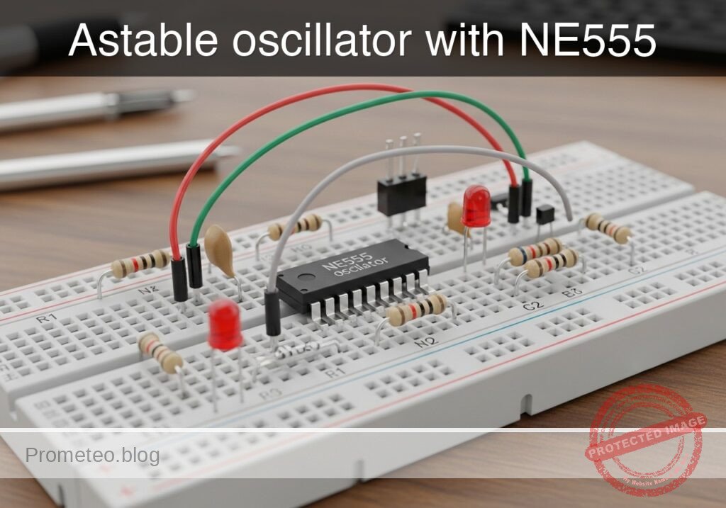
Follow me: