

Level: Basic. Compare switching efficiency and drive requirements of BJT and MOSFET transistors.
Objective and use case
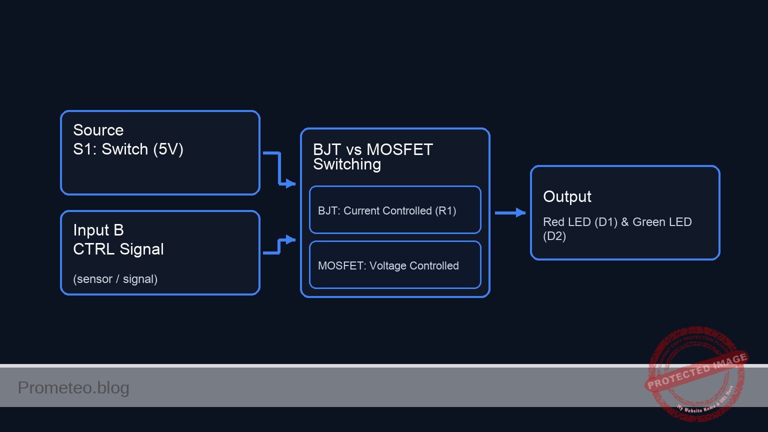
You will build two parallel switching circuits using a BJT (Bipolar Junction Transistor) and a MOSFET (Metal-Oxide-Semiconductor Field-Effect Transistor) to drive identical LED loads. By measuring input currents and output voltage drops, you will observe the fundamental differences in how these devices control power.
Why it is useful:
* Efficiency: Understanding which transistor dissipates less power (heat) in a specific application.
* Microcontroller interfacing: Learning which device connects directly to logic pins without loading the processor.
* Drive requirements: Distinguishing between current-controlled devices (BJT) and voltage-controlled devices (MOSFET).
* Component selection: Making informed decisions for motor drivers, relay controls, and high-power switching.
Expected outcome:
* Input Current: The BJT will draw measurable current into its Base, while the MOSFET Gate current will be near zero.
* Voltage Drop: You will measure different voltage drops (VCE vs VDS) across the transistors when ON.
* LED Action: Both LEDs will light up, visually confirming the switching action.
Target audience and level:
Students and hobbyists learning component characteristics.
Materials
- V1: 5 V DC supply, function: Main power source.
- S1: SPST toggle switch, function: Input control signal.
- Q1: 2N2222 NPN Transistor, function: Current-controlled switch.
- M1: 2N7000 N-Channel MOSFET, function: Voltage-controlled switch.
- R1: 1 kΩ resistor, function: Current limiting for BJT Base.
- R2: 10 kΩ resistor, function: Pull-down for switch signal.
- R3: 330 Ω resistor, function: Current limiting for BJT load (LED).
- R4: 330 Ω resistor, function: Current limiting for MOSFET load (LED).
- D1: Red LED, function: Load indicator for BJT.
- D2: Green LED, function: Load indicator for MOSFET.
Wiring guide
Construct the circuit following these connections using the node names provided.
Control Signal Section:
* S1 connects between node VCC and node CTRL.
* R2 connects between node CTRL and node 0 (GND).
BJT Circuit (Current Controlled):
* R1 connects between node CTRL and node B_BASE.
* Q1 Base connects to node B_BASE.
* Q1 Emitter connects to node 0.
* Q1 Collector connects to node B_COLL.
* D1 Anode connects to node VCC.
* D1 Cathode connects to node D1_K.
* R3 connects between node D1_K and node B_COLL.
MOSFET Circuit (Voltage Controlled):
* M1 Gate connects directly to node CTRL.
* M1 Source connects to node 0.
* M1 Drain connects to node M_DRAIN.
* D2 Anode connects to node VCC.
* D2 Cathode connects to node D2_K.
* R4 connects between node D2_K and node M_DRAIN.
Conceptual block diagram
Schematic
+-------------------------------------------------------------------------+
|               PRACTICAL CASE: COMPARING BJT AND MOSFET SWITCHES         |
+-------------------------------------------------------------------------+

1. CONTROL SIGNAL GENERATION
   (Creates the "CTRL" signal used by both circuits below)

   VCC (5 V) --> [ S1: Switch ] --+--(Node: CTRL)
                                 |
                                 +--> [ R2: 10k Pull-Down ] --> GND


2. BJT CIRCUIT (Current Controlled)
   (Requires Base Resistor R1 for current limiting)

   [ Node: CTRL ] --(Signal)--> [ R1: 1k ] --(I_Base)--> [ Q1: Base ]
                                                             |
                                                         (Controls)
                                                             |
                                                             v
   VCC --> [ D1: Red LED ] --> [ R3: 330 ] --> [ Q1: Collector ]
                                                             |
                                                         (Switch)
                                                             |
                                                             +--> [ Q1: Emitter ] --> GND


3. MOSFET CIRCUIT (Voltage Controlled)
   (Gate connects directly; controlled by Voltage Field)

   [ Node: CTRL ] --(Voltage)--------------------------> [ M1: Gate ]
                                                             |
                                                         (Controls)
                                                             |
                                                             v
   VCC --> [ D2: Grn LED ] --> [ R4: 330 ] --> [ M1: Drain ]
                                                             |
                                                         (Switch)
                                                             |
                                                             +--> [ M1: Source ] --> GND
Measurements and tests
Perform the following steps to validate the differences between the transistors.
- Switch ON: Close switch S1 to apply 5 V to the control node. Ensure both D1 (Red) and D2 (Green) turn on.
- Test 1: Input Current (Current Gain vs. Field Effect):
- Measure the voltage across R1 (1 kΩ). Use Ohm’s Law ($I = V/R$) to calculate the Base current (IB) flowing into Q1.
- Result: You should calculate approximately 4.3 mA.
- Try to measure current flowing into the Gate of M1.
- Result: It should be effectively 0 mA (typically nano-amps), proving the MOSFET is voltage-controlled.
- Test 2: Switching Efficiency (Voltage Drop):
- Measure the voltage from Q1 Collector to Emitter (VCE).
- Result: Expect a drop of roughly 0.1 V to 0.2 V (Saturation voltage).
- Measure the voltage from M1 Drain to Source (VDS).
- Result: For small currents with a 2N7000, this drop is often very low (millivolts), dependent on Iload × Rdson.
SPICE netlist and simulation
Reference SPICE Netlist (ngspice) — excerptFull SPICE netlist (ngspice)
* Practical case: Comparing BJT and MOSFET Switches
.width out=256

* --- Power Supply ---
* V1: Main 5V DC supply
V1 VCC 0 DC 5

* --- Control Signal Section ---
* S1: SPST toggle switch connecting VCC to CTRL.
* Modeled as a voltage-controlled switch (S1) driven by a behavioral pulse source (V_SW_ACT)
* to simulate the user pressing the button periodically.
V_SW_ACT SW_CTRL 0 PULSE(0 5 10u 1u 1u 100u 200u)
S1 VCC CTRL SW_CTRL 0 SWITCH_MOD

* R2: Pull-down resistor (10k) ensures CTRL goes to 0V when switch is open
R2 CTRL 0 10k

* --- BJT Circuit (Current Controlled) ---
* R1: Current limiting resistor for Base (1k)
R1 CTRL B_BASE 1k
* ... (truncated in public view) ...
Copy this content into a .cir file and run with ngspice.
* Practical case: Comparing BJT and MOSFET Switches
.width out=256

* --- Power Supply ---
* V1: Main 5V DC supply
V1 VCC 0 DC 5

* --- Control Signal Section ---
* S1: SPST toggle switch connecting VCC to CTRL.
* Modeled as a voltage-controlled switch (S1) driven by a behavioral pulse source (V_SW_ACT)
* to simulate the user pressing the button periodically.
V_SW_ACT SW_CTRL 0 PULSE(0 5 10u 1u 1u 100u 200u)
S1 VCC CTRL SW_CTRL 0 SWITCH_MOD

* R2: Pull-down resistor (10k) ensures CTRL goes to 0V when switch is open
R2 CTRL 0 10k

* --- BJT Circuit (Current Controlled) ---
* R1: Current limiting resistor for Base (1k)
R1 CTRL B_BASE 1k

* Q1: 2N2222 NPN Transistor
* Syntax: Qname Collector Base Emitter Model
Q1 B_COLL B_BASE 0 2N2222

* BJT Load Indicator: Red LED (D1) and Resistor (R3)
* D1 Anode connects to VCC, Cathode to D1_K
D1 VCC D1_K LED_RED
* R3 connects between D1_K and BJT Collector
R3 D1_K B_COLL 330

* --- MOSFET Circuit (Voltage Controlled) ---
* M1: 2N7000 N-Channel MOSFET
* Syntax: Mname Drain Gate Source Bulk Model
M1 M_DRAIN CTRL 0 0 2N7000

* MOSFET Load Indicator: Green LED (D2) and Resistor (R4)
* D2 Anode connects to VCC, Cathode to D2_K
D2 VCC D2_K LED_GREEN
* R4 connects between D2_K and MOSFET Drain
R4 D2_K M_DRAIN 330

* --- Component Models ---

* Switch Model (Threshold 2.5V, Low On-Resistance)
.model SWITCH_MOD SW(Vt=2.5 Ron=0.1 Roff=10Meg)

* BJT Model (Standard 2N2222 parameters)
.model 2N2222 NPN(IS=1E-14 BF=200 VAF=100 IKF=0.3 XTB=1.5 BR=3 CJC=8p CJE=25p TR=46n TF=411p RC=0.3 RE=0.2)

* MOSFET Model (2N7000 approximation Level 1)
.model 2N7000 NMOS(Level=1 VTO=2.1 KP=0.12 LAMBDA=0.01 RD=1 RS=1 CGSO=10p CGDO=10p CGBO=10p)

* LED Models (Generic Red and Green)
* Red LED approx 1.8V drop
.model LED_RED D(IS=1e-20 N=2.0 RS=5 BV=5 IBV=10u CJO=10p)
* Green LED approx 2.1V drop
.model LED_GREEN D(IS=1e-22 N=1.5 RS=5 BV=5 IBV=10u CJO=10p)

* --- Analysis Directives ---
.op
* Transient analysis: 1us step, 500us duration (captures 2.5 cycles of 200us pulse)
.tran 1u 500u

* Output Print Directives
* Order: Input (CTRL), BJT Output (Collector), MOSFET Output (Drain)
.print tran V(CTRL) V(B_COLL) V(M_DRAIN)

.end
Simulation Results (Transient Analysis)

Show raw data table (638 rows)
Index   time            v(ctrl)         v(b_coll)       v(m_drain)
0	0.000000e+00	4.995044e-03	3.947532e+00	4.062211e+00
1	1.000000e-08	4.995044e-03	3.947532e+00	4.062211e+00
2	2.000000e-08	4.995044e-03	3.947532e+00	4.062211e+00
3	4.000000e-08	4.995044e-03	3.947532e+00	4.062211e+00
4	8.000000e-08	4.995044e-03	3.947532e+00	4.062211e+00
5	1.600000e-07	4.995044e-03	3.947532e+00	4.062211e+00
6	3.200000e-07	4.995044e-03	3.947532e+00	4.062211e+00
7	6.400000e-07	4.995044e-03	3.947532e+00	4.062211e+00
8	1.280000e-06	4.995044e-03	3.947532e+00	4.062211e+00
9	2.280000e-06	4.995044e-03	3.947532e+00	4.062211e+00
10	3.280000e-06	4.995044e-03	3.947532e+00	4.062211e+00
11	4.280000e-06	4.995044e-03	3.947532e+00	4.062211e+00
12	5.280000e-06	4.995044e-03	3.947532e+00	4.062211e+00
13	6.280000e-06	4.995044e-03	3.947532e+00	4.062211e+00
14	7.280000e-06	4.995044e-03	3.947532e+00	4.062211e+00
15	8.280000e-06	4.995044e-03	3.947532e+00	4.062211e+00
16	9.280000e-06	4.995044e-03	3.947532e+00	4.062211e+00
17	1.000000e-05	4.995044e-03	3.947532e+00	4.062211e+00
18	1.010000e-05	4.995044e-03	3.947532e+00	4.062211e+00
19	1.026000e-05	4.995044e-03	3.947532e+00	4.062211e+00
20	1.030750e-05	4.995044e-03	3.947532e+00	4.062211e+00
21	1.039062e-05	4.995044e-03	3.947532e+00	4.062211e+00
22	1.041363e-05	4.995044e-03	3.947532e+00	4.062211e+00
23	1.045390e-05	4.995044e-03	3.947532e+00	4.062211e+00
... (614 more rows) ...
Common mistakes and how to avoid them
- Omitting the Base Resistor (R1): Connecting 5 V directly to the BJT Base will destroy the transistor immediately due to excessive current. Always use a limiting resistor.
- Floating the MOSFET Gate: If R2 (pull-down) is removed and S1 is open, the MOSFET may turn on/off randomly due to static charge. Always tie the Gate to a known level.
- Pinout Confusion: Mixing up the Drain/Source on the MOSFET or Collector/Emitter on the BJT. Always check the datasheet diagram for the specific package (TO-92).
Troubleshooting
- Symptom: BJT gets hot, but LED is dim.
- Cause: The transistor is in the active region (not fully saturated) or R1 is too high.
- Fix: Decrease R1 slightly to ensure enough Base current drives the transistor into saturation.
- Symptom: MOSFET does not turn on.
- Cause: Gate Threshold Voltage (Vgsth) is higher than the supply voltage.
- Fix: Ensure the 2N7000 is used (logic level compatible) or check that the supply is at least 5 V.
- Symptom: LEDs stay on when S1 is open.
- Cause: Missing pull-down resistor R2.
- Fix: Install R2 (10 kΩ) to discharge the node
CTRLto ground when the switch is open.
Possible improvements and extensions
- Inductive Load Test: Replace the LEDs/Resistors with small 5 V DC motors. Add flyback diodes (e.g., 1N4007) across the motors to protect the transistors from voltage spikes.
- High Power Comparison: Swap Q1 for a TIP31 and M1 for an IRF520 to drive a heavier load (like a 12 V 10W lamp). Observe which component requires a heatsink first (typically the BJT).
More Practical Cases on Prometeo.blog
Find this product and/or books on this topic on Amazon
As an Amazon Associate, I earn from qualifying purchases. If you buy through this link, you help keep this project running.
Quick Quiz

Telecommunications Electronics Engineer and Computer Engineer (official degrees in Spain).

