Level: Basic – Build a logic circuit that activates an alarm only when two security keys are turned simultaneously.
Objective and use case
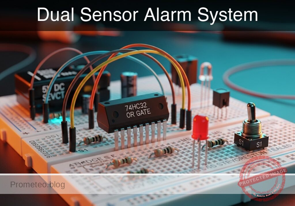
In this project, you will build a digital safety interlock circuit using a 74HC08 Quad 2-Input AND Gate. The system mimics a high-security protocol where a mechanism (represented by an LED) activates only if two separate inputs (switches) are triggered at the exact same time.
-
Real-world applications:
- Industrial machinery: Safety presses requiring the operator to place both hands on separate buttons to prevent injury.
- Bank vaults: Dual-key requirements where two managers must be present to open a safe.
- Aerospace: Launch control systems requiring dual confirmation commands.
- Home Automation: «Smart» lock logic where biometric data and a PIN code must both match.
-
Expected outcome:
- Idle State: LED remains completely OFF (Logic Low, < 0.1 V) when switches are open.
- Single Activation: LED remains OFF if only Switch A or only Switch B is closed.
- Active State: LED turns ON (Logic High, > 3.5 V) exclusively when Switch A AND Switch B are closed.
- Visual: A clear, stable light signal indicating «Access Granted.»
-
Target audience and level: Students exploring digital logic basics and the 7400 IC family.
Materials
- U1: 74HC08 Quad 2-Input AND Gate IC.
- S1: SPST toggle switch or push button, function: Security Key A.
- S2: SPST toggle switch or push button, function: Security Key B.
- R1: 10 kΩ resistor, function: pull-down resistor for Input A.
- R2: 10 kΩ resistor, function: pull-down resistor for Input B.
- R3: 330 Ω resistor, function: LED current limiting.
- D1: Red LED, function: System Status Indicator.
- V1: 5 V DC power supply.
Pin-out of the IC used
Selected Chip: 74HC08 (Quad 2-Input AND Gate)
| Pin | Name | Logic Function | Connection in this case |
|---|---|---|---|
| 1 | 1A | Input A (Gate 1) | Connected to S1 node (VA) |
| 2 | 1B | Input B (Gate 1) | Connected to S2 node (VB) |
| 3 | 1Y | Output (Gate 1) | Connected to LED driver node (VOUT) |
| 7 | GND | Ground | Connected to 0 V |
| 14 | VCC | Power Supply | Connected to +5 V |
(Note: Pins 4, 5, 6, 8, 9, 10, 11, 12, 13 are unused in this single-gate implementation but inputs should technically be grounded in a permanent PCB design to prevent noise.)
Wiring guide
Follow this node-based connection guide to assemble the circuit on your breadboard.
-
Power Rail Connections:
- Connect V1 positive terminal to node
VCC. - Connect V1 negative terminal to node
0(GND). - Connect U1 Pin 14 to
VCC. - Connect U1 Pin 7 to
0.
- Connect V1 positive terminal to node
-
Input Stage (Switch A):
- Connect S1 between node
VCCand nodeVA. - Connect R1 between node
VAand node0(this ensuresVAis Low when S1 is open). - Connect U1 Pin 1 to node
VA.
- Connect S1 between node
-
Input Stage (Switch B):
- Connect S2 between node
VCCand nodeVB. - Connect R2 between node
VBand node0(this ensuresVBis Low when S2 is open). - Connect U1 Pin 2 to node
VB.
- Connect S2 between node
-
Output Stage:
- Connect U1 Pin 3 to node
VOUT. - Connect R3 between node
VOUTand the Anode of D1. - Connect the Cathode of D1 to node
0.
- Connect U1 Pin 3 to node
Conceptual block diagram
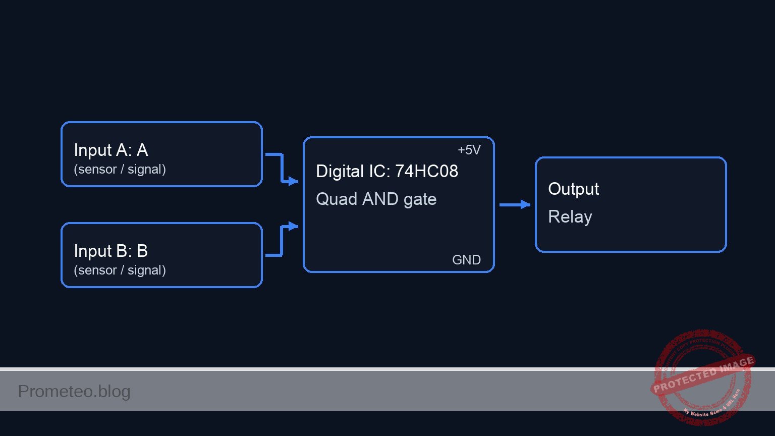
Schematic
[ INPUTS ]                                [ LOGIC ]                         [ OUTPUT ]

 [ VCC ] -> [ S1: Key A ] --+--(Node VA)-->+-------------------+
                            |              |  Pin 1            |
                       [ R1: 10k ]         |                   |
                            v              |    U1: 74HC08     |
                         [ GND ]           |    (AND Gate)     |--(Pin 3)--> [ R3: 330 Ω ] --> [ D1: LED ] --> [ GND ]
                                           |                   |
 [ VCC ] -> [ S2: Key B ] --+--(Node VB)-->+-------------------+
                            |                 Pin 2
                       [ R2: 10k ]
                            v
                         [ GND ]
Truth table
The 74HC08 follows standard positive boolean logic (A AND B).
| Key A (S1) | Key B (S2) | Input A (Pin 1) | Input B (Pin 2) | Output Y (Pin 3) | LED Status |
|---|---|---|---|---|---|
| Open | Open | 0 (Low) | 0 (Low) | 0 (Low) | OFF |
| Open | Closed | 0 (Low) | 1 (High) | 0 (Low) | OFF |
| Closed | Open | 1 (High) | 0 (Low) | 0 (Low) | OFF |
| Closed | Closed | 1 (High) | 1 (High) | 1 (High) | ON |
Measurements and tests
- Supply Check: Use a multimeter to verify 5 V between
VCCand0on the breadboard rails. - Input Verification:
- Keep S1 open: Measure voltage at
VA. It should be 0 V. - Close S1: Measure voltage at
VA. It should be ~5 V. - Repeat for S2 and
VB.
- Keep S1 open: Measure voltage at
- Logic Logic Verification:
- Close S1 only. Measure
VOUTat Pin 3. Expected: ~0 V. - Close S2 only. Measure
VOUTat Pin 3. Expected: ~0 V. - Close both S1 and S2. Measure
VOUT. Expected: > 3.5 V (High Logic).
- Close S1 only. Measure
- Current Draw (Optional): Measure the current through R3 when the LED is ON. It should be approximately 8–10 mA.
SPICE netlist and simulation
Reference SPICE Netlist (ngspice) — excerptFull SPICE netlist (ngspice)
* Practical case: Double Key Security System

* --- Power Supply ---
* V1: 5V DC Power Supply connected to VCC and GND (0)
V1 VCC 0 DC 5

* --- Input Stage (Switch A) ---
* User actuation simulation for Switch A (Control Signal)
* Generates a pulse sequence to test logic states.
* Logic sequence plan: 00 -> 01 -> 10 -> 11
* Actuation A: Low for 100us, High for 100us.
V_ACT_A ACT_A 0 PULSE(0 5 100u 1u 1u 99u 200u)

* S1: SPST Switch connecting VCC to VA when actuated
S1 VCC VA ACT_A 0 SW_PUSHBUTTON

* R1: 10k Pull-down resistor for Input A
R1 VA 0 10k

* --- Input Stage (Switch B) ---
* User actuation simulation for Switch B (Control Signal)
* Actuation B: Toggles every 50us.
V_ACT_B ACT_B 0 PULSE(0 5 50u 1u 1u 49u 100u)

* S2: SPST Switch connecting VCC to VB when actuated
S2 VCC VB ACT_B 0 SW_PUSHBUTTON

* R2: 10k Pull-down resistor for Input B
R2 VB 0 10k

* ... (truncated in public view) ...
Copy this content into a .cir file and run with ngspice.
* Practical case: Double Key Security System

* --- Power Supply ---
* V1: 5V DC Power Supply connected to VCC and GND (0)
V1 VCC 0 DC 5

* --- Input Stage (Switch A) ---
* User actuation simulation for Switch A (Control Signal)
* Generates a pulse sequence to test logic states.
* Logic sequence plan: 00 -> 01 -> 10 -> 11
* Actuation A: Low for 100us, High for 100us.
V_ACT_A ACT_A 0 PULSE(0 5 100u 1u 1u 99u 200u)

* S1: SPST Switch connecting VCC to VA when actuated
S1 VCC VA ACT_A 0 SW_PUSHBUTTON

* R1: 10k Pull-down resistor for Input A
R1 VA 0 10k

* --- Input Stage (Switch B) ---
* User actuation simulation for Switch B (Control Signal)
* Actuation B: Toggles every 50us.
V_ACT_B ACT_B 0 PULSE(0 5 50u 1u 1u 49u 100u)

* S2: SPST Switch connecting VCC to VB when actuated
S2 VCC VB ACT_B 0 SW_PUSHBUTTON

* R2: 10k Pull-down resistor for Input B
R2 VB 0 10k

* --- Logic Stage (U1: 74HC08) ---
* Quad 2-Input AND Gate. Using 1 gate (Pins 1, 2, 3).
* Connections: Pin1=VA, Pin2=VB, Pin3=VOUT, Pin7=GND, Pin14=VCC
XU1 VA VB VOUT 0 VCC 74HC08

* --- Output Stage ---
* R3: 330 Ohm Current Limiting Resistor
R3 VOUT LED_ANODE 330

* D1: Red LED System Status Indicator
D1 LED_ANODE 0 DLED

* --- Models ---

* Switch Model (Voltage Controlled Switch)
* Vt=2.5V threshold, Low resistance when ON, High when OFF
.model SW_PUSHBUTTON SW(Vt=2.5 Ron=1 Roff=100Meg)

* LED Model
.model DLED D(IS=1e-14 N=2 RS=10 BV=5)

* 74HC08 Subcircuit Model (Behavioral AND Gate)
* Implements Vout = VCC * AND(A, B) using continuous sigmoid functions for convergence
* Pins: 1=A, 2=B, 3=Y, 7=GND, 14=VCC
.subckt 74HC08 P1 P2 P3 P7 P14
* Behavioral Source B1: Logic AND function
* Sigmoid function: 1 / (1 + exp(-k*(V-Vth)))
* k=50 provides sharp transition, Vth=2.5V
B1 P3 P7 V = V(P14, P7) * (1 / (1 + exp(-50 * (V(P1, P7) - 2.5)))) * (1 / (1 + exp(-50 * (V(P2, P7) - 2.5))))
.ends

* --- Simulation Commands ---
* Transient analysis for 250us to cover all logic states (00, 01, 10, 11)
.tran 1u 250u

* Print directives for logging
.print tran V(VA) V(VB) V(VOUT)

* Calculate DC operating point
.op

.end
Simulation Results (Transient Analysis)

Show raw data table (322 rows)
Index   time            v(va)           v(vb)           v(vout)
0	0.000000e+00	4.999500e-04	4.999500e-04	1.403014e-108
1	1.000000e-08	4.999500e-04	4.999500e-04	1.403014e-108
2	2.000000e-08	4.999500e-04	4.999500e-04	1.403014e-108
3	4.000000e-08	4.999500e-04	4.999500e-04	1.403014e-108
4	8.000000e-08	4.999500e-04	4.999500e-04	1.403014e-108
5	1.600000e-07	4.999500e-04	4.999500e-04	1.403014e-108
6	3.200000e-07	4.999500e-04	4.999500e-04	1.403014e-108
7	6.400000e-07	4.999500e-04	4.999500e-04	1.403014e-108
8	1.280000e-06	4.999500e-04	4.999500e-04	1.403014e-108
9	2.280000e-06	4.999500e-04	4.999500e-04	1.403014e-108
10	3.280000e-06	4.999500e-04	4.999500e-04	1.403014e-108
11	4.280000e-06	4.999500e-04	4.999500e-04	1.403014e-108
12	5.280000e-06	4.999500e-04	4.999500e-04	1.403014e-108
13	6.280000e-06	4.999500e-04	4.999500e-04	1.403014e-108
14	7.280000e-06	4.999500e-04	4.999500e-04	1.403014e-108
15	8.280000e-06	4.999500e-04	4.999500e-04	1.403014e-108
16	9.280000e-06	4.999500e-04	4.999500e-04	1.403014e-108
17	1.028000e-05	4.999500e-04	4.999500e-04	1.403014e-108
18	1.128000e-05	4.999500e-04	4.999500e-04	1.403014e-108
19	1.228000e-05	4.999500e-04	4.999500e-04	1.403014e-108
20	1.328000e-05	4.999500e-04	4.999500e-04	1.403014e-108
21	1.428000e-05	4.999500e-04	4.999500e-04	1.403014e-108
22	1.528000e-05	4.999500e-04	4.999500e-04	1.403014e-108
23	1.628000e-05	4.999500e-04	4.999500e-04	1.403014e-108
... (298 more rows) ...
Common mistakes and how to avoid them
- Floating Inputs: Forgetting resistors R1 or R2. Without them, the inputs «float» and may pick up static noise, causing the LED to flicker randomly even when switches are open.
- Missing Power to IC: Forgetting to connect Pin 14 to VCC and Pin 7 to GND. The chip will not function and may overheat if inputs are driven while the chip is unpowered.
- LED Polarity: Inserting D1 backward (Anode to Ground). The LED will never light up, even if the logic is correct.
Troubleshooting
-
Symptom: LED is always ON, regardless of switch position.
- Cause: Input resistors (R1/R2) might be connected to VCC instead of GND, or the switch is wired incorrectly (shorting VCC to Input directly).
- Fix: Check that R1 and R2 connect the inputs to Ground (Pull-down configuration).
-
Symptom: LED flickers when I touch the wires.
- Cause: Floating input pin.
- Fix: Ensure the pull-down resistors are firmly seated in the breadboard and making contact.
-
Symptom: LED is very dim when both switches are pressed.
- Cause: R3 value is too high (e.g., 10 kΩ instead of 330 Ω) or the supply voltage is too low.
- Fix: Replace R3 with a 220 Ω or 330 Ω resistor.
Possible improvements and extensions
- Triple Security: Replace the 74HC08 with a 74HC11 (Triple 3-Input AND Gate) to require three simultaneous keys.
- High Power Output: Connect the output
VOUTto an NPN transistor (like 2N2222) or a Relay Module to drive a loud siren or a 12V motor instead of a small LED.
More Practical Cases on Prometeo.blog
Find this product and/or books on this topic on Amazon
As an Amazon Associate, I earn from qualifying purchases. If you buy through this link, you help keep this project running.
Quick Quiz

Telecommunications Electronics Engineer and Computer Engineer (official degrees in Spain).