
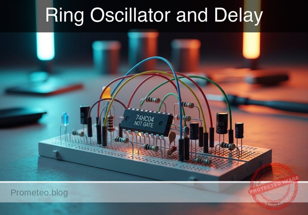
Level: Advanced — Build and analyze a 5-stage ring oscillator to calculate component propagation delay.
Objective and use case
In this case, you will construct a ring oscillator by cascading an odd number (5) of NOT gates (inverters) in a closed feedback loop using a 74HC04 IC. You will measure the resulting oscillation frequency to calculate the intrinsic propagation delay of the logic gates.
Why it is useful:
* Process characterization: Used in semiconductor manufacturing to test the speed and quality of silicon wafers.
* Clock generation: Fundamental topology for generating internal clocks in ASICs and FPGAs.
* Random Number Generation: The inherent jitter in ring oscillators is a source of entropy for True Random Number Generators (TRNG).
* Time-to-Digital Converters (TDC): Used to measure time intervals with high precision.
Expected outcome:
* A stable square wave output oscillating in the MHz range (typically 20 MHz–50 MHz for 74HC logic on a breadboard).
* Measurement of oscillation frequency (fosc).
* Calculation of the average propagation delay (tpd) per gate.
* Visual observation of rise (tr) and fall (tf) times due to capacitive loading.
Target audience and level:
Advanced Electronics Students; Engineering Undergraduates.
Materials
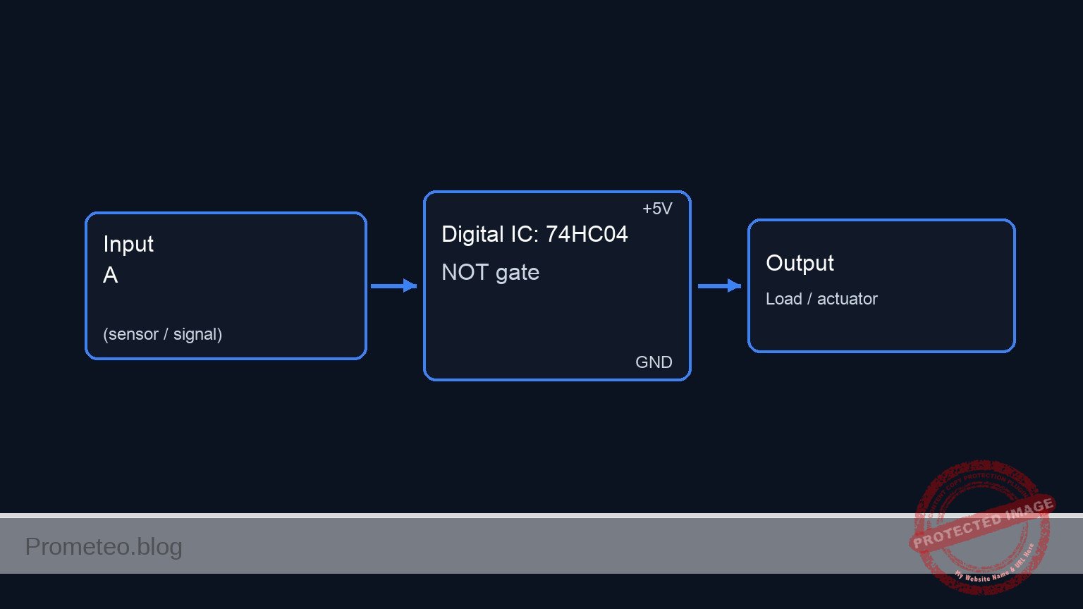
- U1: 74HC04 Hex Inverter IC, function: logic gates for the ring
- C1: 100 nF ceramic capacitor, function: power supply decoupling (critical for stability)
- C2: 10 pF capacitor, function: simulated load (optional, represents probe capacitance)
- V1: 5 V DC supply
- W1-W5: Jumper wires, function: inter-stage connections
Pin-out of the IC used
Selected Chip: 74HC04 (Hex Inverter)
| Pin | Name | Logic function | Connection in this case |
|---|---|---|---|
| 1 | 1 A | Input 1 | From Output 5 (Node N5) |
| 2 | 1Y | Output 1 | To Input 2 (Node N1) |
| 3 | 2 A | Input 2 | From Output 1 (Node N1) |
| 4 | 2Y | Output 2 | To Input 3 (Node N2) |
| 5 | 3 A | Input 3 | From Output 2 (Node N2) |
| 6 | 3Y | Output 3 | To Input 4 (Node N3) |
| 7 | GND | Ground | Connect to Node 0 |
| 8 | 4Y | Output 4 | To Input 5 (Node N4) |
| 9 | 4 A | Input 4 | From Output 3 (Node N3) |
| 10 | 5Y | Output 5 | To Input 1 (Node N5 – Feedback) |
| 11 | 5 A | Input 5 | From Output 4 (Node N4) |
| 14 | VCC | Power Supply | Connect to Node VCC (+5 V) |
Note: Pins 12 (6Y) and 13 (6 A) are unused and should be left open or tied to GND/VCC depending on specific noise requirements, though for this test leaving them open is acceptable.
Wiring guide
This circuit relies on minimal trace length to sustain high-frequency oscillation.
- V1 connects between node
VCCand node0(GND). - C1 connects between node
VCCand node0(place physically close to U1). - U1 (Pin 14) connects to node
VCC. - U1 (Pin 7) connects to node
0. - U1 (Pin 1 – Input 1) connects to node
N5(Feedback loop closure). - U1 (Pin 2 – Output 1) connects to node
N1. - U1 (Pin 3 – Input 2) connects to node
N1. - U1 (Pin 4 – Output 2) connects to node
N2. - U1 (Pin 5 – Input 3) connects to node
N2. - U1 (Pin 6 – Output 3) connects to node
N3. - U1 (Pin 9 – Input 4) connects to node
N3. - U1 (Pin 8 – Output 4) connects to node
N4. - U1 (Pin 11 – Input 5) connects to node
N4. - U1 (Pin 10 – Output 5) connects to node
N5. - C2 (Optional Load) connects between node
N5and node0to simulate probe capacitance.
Conceptual block diagram
Schematic
POWER SUPPLY & DECOUPLING:
      VCC (5 V) --> [ Node VCC ] --(Pin 14)--> [ U1: 74HC04 Power ]
                      |
                    [ C1: 100nF ]
                      |
      GND (0 V) --> [ Node 0 ] --(Pin 7)---> [ U1: 74HC04 GND ]


SIGNAL FLOW (RING OSCILLATOR):
(Logic flows Left to Right, wrapping around at the end)

      [ Feedback N5 ] --> [ U1: Gate 1 ] --(Node N1)--> [ U1: Gate 2 ] --(Node N2)--> [ U1: Gate 3 ] --(Node N3)--> \
      (Input Pin 1)       (In:1 / Out:2)                (In:3 / Out:4)                (In:5 / Out:6)                |
                                                                                                                    |
      /-------------------------------------------------------------------------------------------------------------/
      |
      \--> [ U1: Gate 4 ] --(Node N4)--> [ U1: Gate 5 ] --(Node N5)--> [ C2: 10pF ] --> GND
           (In:9 / Out:8)                (In:11 / Out:10)      |
                                                               |
                                                      (Loop back to Start)
Truth table (Single NOT Gate)
| Input (A) | Output (Y) |
|---|---|
| L | H |
| H | L |
In a ring configuration with an odd number of stages, the logic never settles, causing perpetual oscillation.
Measurements and tests
- Setup: Ensure wiring is short and neat. Long wires add parasitic inductance and capacitance which will significantly lower the frequency.
- Visualization: Connect an oscilloscope probe (x10 attenuation recommended to reduce loading) to Node
N5(or any nodeN1throughN4). - Frequency Measurement: Measure the frequency of the oscillation (fosc). For a 74HC series at 5 V, expect approx 20MHz – 40MHz depending on stray capacitance.
- Propagation Delay Calculation: Calculate the average propagation delay per gate (tpd) using the formula:
$tpd = (1 / (2 × N × fosc))$
Where $N = 5$ (number of stages).
Example: If $f_{osc} = 25 MHz$, then $T = 40 ns$. $t_{pd} = 40 ns / 10 = 4 ns$. - Waveform Analysis: Zoom in on the edges. Notice that the wave is not a perfect square; the rise time ($t_{r}$) and fall time ($t_{f}$) are visible due to the capacitive charging of the next gate’s input.
SPICE netlist and simulation
Reference SPICE Netlist (ngspice)
* Practical case: Ring Oscillator and Delay
.width out=256
* Ngspice Netlist

* --- Power Supply ---
* V1: 5 V DC supply connecting VCC to GND (0)
V1 VCC 0 DC 5

* --- Decoupling Capacitor ---
* C1: 100 nF ceramic capacitor, power supply decoupling
C1 VCC 0 100n

* --- Integrated Circuit U1: 74HC04 Hex Inverter ---
* Modeled as a subcircuit to strictly follow physical pinout and wiring guide.
* Pin Mapping (Standard DIP-14):
* 1:1A  2:1Y  3:2A  4:2Y  5:3A  6:3Y  7:GND
* 8:4Y  9:4A 10:5Y 11:5A 12:6Y 13:6A 14:VCC
*
* Wiring Connections based on Guide:
* Pin 1 (In1)  -> N5
* ... (truncated in public view) ...
Copy this content into a .cir file and run with ngspice.
Simulation Results (Transient Analysis)

Show raw data table (2039 rows)
Index   time            v(n5)           v(n1)           v(n2)           v(n3)           v(n4)
0	1.000000e-11	5.000000e+00	5.000000e+00	5.000000e+00	5.000000e+00	5.000000e+00
1	1.028000e-11	5.000000e+00	5.000000e+00	5.000000e+00	5.000000e+00	5.000000e+00
2	1.084000e-11	5.000000e+00	5.000000e+00	5.000000e+00	5.000000e+00	5.000000e+00
3	1.196000e-11	5.000000e+00	5.000000e+00	5.000000e+00	5.000000e+00	5.000000e+00
4	1.420000e-11	5.000000e+00	5.000000e+00	5.000000e+00	5.000000e+00	5.000000e+00
5	1.868000e-11	5.000000e+00	5.000000e+00	5.000000e+00	5.000000e+00	5.000000e+00
6	2.764000e-11	5.000000e+00	5.000000e+00	5.000000e+00	5.000000e+00	5.000000e+00
7	4.556000e-11	5.000000e+00	5.000000e+00	5.000000e+00	5.000000e+00	5.000000e+00
8	8.140000e-11	5.000000e+00	5.000000e+00	5.000000e+00	5.000000e+00	5.000000e+00
9	1.530800e-10	5.000000e+00	5.000000e+00	5.000000e+00	5.000000e+00	5.000000e+00
10	2.964400e-10	5.000000e+00	5.000000e+00	5.000000e+00	5.000000e+00	5.000000e+00
11	5.831600e-10	5.000000e+00	5.000000e+00	5.000000e+00	5.000000e+00	5.000000e+00
12	1.000000e-09	5.000000e+00	5.000000e+00	5.000000e+00	5.000000e+00	5.000000e+00
13	1.057344e-09	5.000000e+00	5.000000e+00	5.000000e+00	5.000000e+00	5.000000e+00
14	1.172032e-09	5.000000e+00	5.000000e+00	5.000000e+00	5.000000e+00	5.000000e+00
15	1.401408e-09	5.000000e+00	5.000000e+00	5.000000e+00	5.000000e+00	5.000000e+00
16	1.860160e-09	5.000000e+00	5.000000e+00	5.000000e+00	5.000000e+00	5.000000e+00
17	2.777664e-09	4.999998e+00	4.999998e+00	4.999998e+00	4.999998e+00	4.999998e+00
18	3.777664e-09	4.999526e+00	4.999526e+00	4.999526e+00	4.999526e+00	4.999526e+00
19	4.777664e-09	4.987728e+00	4.987728e+00	4.987728e+00	4.987728e+00	4.987728e+00
20	5.777664e-09	4.795985e+00	4.795985e+00	4.795985e+00	4.795985e+00	4.795985e+00
21	6.777664e-09	3.794650e+00	3.794650e+00	3.794650e+00	3.794650e+00	3.794650e+00
22	7.777664e-09	2.828762e+00	2.828762e+00	2.828762e+00	2.828762e+00	2.828762e+00
23	8.777664e-09	2.564867e+00	2.564867e+00	2.564867e+00	2.564867e+00	2.564867e+00
... (2015 more rows) ...
Common mistakes and how to avoid them
- Using an even number of gates: If you use 4 or 6 gates, the logic will settle into a stable state (latch up) rather than oscillate. Always use an odd number (3, 5, 7…).
- Breadboard capacitance: Standard breadboards have high parasitic capacitance between rows (approx 2-5pF). This will make the oscillator run slower than the datasheet specs imply. Avoid long jumper loops.
- Missing decoupling capacitor: Without C1 close to the chip, the high-frequency switching current will cause VCC sag, resulting in erratic frequency or no oscillation.
Troubleshooting
- Output is stuck High or Low: Check that you have an odd number of inverters in the loop. Verify the feedback wire connects the last output to the first input.
- Frequency is unstable (jitter): Likely power supply noise. Ensure C1 (100nF) is installed extremely close to pins 14 and 7.
- Scope shows a sine wave instead of square: At very high frequencies (approaching the bandwidth limit of the scope or probe), square waves look like sine waves due to the attenuation of higher harmonics. Ensure your scope bandwidth is at least 100 MHz.
- Circuit gets hot: Check for short circuits between outputs. Never connect two outputs together.
Possible improvements and extensions
- Enable Control: Replace the first inverter with a NAND gate (e.g., using 74HC00). Use one input for the feedback loop and the other as an Enable/Disable control signal.
- Buffered Output: Use the 6th unused inverter in the 74HC04 package as a buffer connected to one of the ring nodes. Connect your probe/load to this buffer output. This isolates the ring oscillator from the load capacitance, providing a more accurate frequency measurement.
More Practical Cases on Prometeo.blog
Find this product and/or books on this topic on Amazon
As an Amazon Associate, I earn from qualifying purchases. If you buy through this link, you help keep this project running.
Quick Quiz

Telecommunications Electronics Engineer and Computer Engineer (official degrees in Spain).

