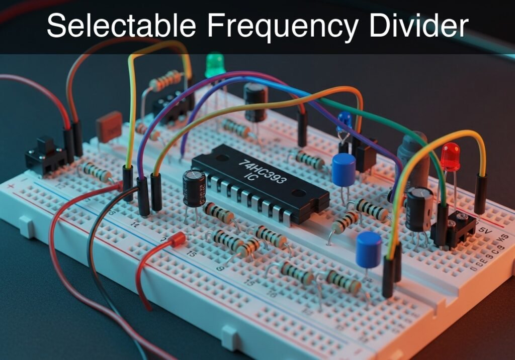
Practical case: Selectable Frequency Divider

Selectable Frequency Divider prototype (Maker Style)

Level: Medium – Build a binary frequency divider using a 74HC393 ripple counter with a selectable output stage.

Objective and use case

You will construct a binary ripple counter circuit utilizing the 74HC393 integrated circuit to process a high-speed input clock. By dividing the frequency by factors of 2, 4, 8, and 16, a physical jumper acts as a selector to route a specific down-scaled output to a visual LED indicator.

This topology is highly useful in practical electronics for several reasons:
* Generating precise, slow timebases for digital clocks from high-frequency crystal oscillators.
* Stepping down high-frequency PWM signals for specific motor control applications.
* Creating multiple synchronized sub-harmonic frequencies for audio synthesizers.
* Converting a rapidly blinking indicator into a manageable, visually observable pulse.

Expected outcomes:
* The CLK input will receive a constant square wave.
* The outputs QA, QB, QC, and QD will cleanly toggle at exactly 1/2, 1/4, 1/8, and 1/16 of the clock frequency, respectively.
* Selecting different outputs via the jumper will visibly change the LED blink rate without altering the main clock source.

Target audience and level: Electronics students and hobbyists wanting hands-on experience with asynchronous logic and frequency scaling.

Materials

  • V1: 5 V DC power supply, function: logic power source
  • VCLK: 5 V square wave clock source (e.g., function generator), function: input clock
  • U1: 74HC393 Dual 4-Bit Binary Ripple Counter, function: frequency divider
  • J1: 4-pin header block with jumper shunt, function: output selector
  • R1: 330 Ω resistor, function: LED current limiting
  • D1: Red LED, function: selected output state indicator

Pin-out of the IC used

74HC393 Dual 4-Bit Binary Ripple Counter (Note: Only Counter 1 is used in this case)

Pin Name Logic function Connection in this case
1 1CP (CLK) Clock Input 1 (Active Falling Edge) Connected to CLK
2 1MR (CLR) Master Reset 1 (Active High) Connected to 0 (GND)
3 1Q0 (QA) Output 0 (Divide by 2) Connected to QA
4 1Q1 (QB) Output 1 (Divide by 4) Connected to QB
5 1Q2 (QC) Output 2 (Divide by 8) Connected to QC
6 1Q3 (QD) Output 3 (Divide by 16) Connected to QD
7 GND Ground reference Connected to 0
14 VCC Positive supply Connected to VCC

Wiring guide

  • V1: connects between node VCC and node 0.
  • VCLK: connects between node CLK and node 0.
  • U1 Pin 14 (VCC): connects to node VCC.
  • U1 Pin 7 (GND): connects to node 0.
  • U1 Pin 1 (1CP): connects to node CLK.
  • U1 Pin 2 (1MR): connects to node 0.
  • U1 Pin 3 (1Q0): connects to node QA and selector terminal 1 of J1.
  • U1 Pin 4 (1Q1): connects to node QB and selector terminal 2 of J1.
  • U1 Pin 5 (1Q2): connects to node QC and selector terminal 3 of J1.
  • U1 Pin 6 (1Q3): connects to node QD and selector terminal 4 of J1.
  • J1 common terminal: connects to node VOUT.
  • R1: connects between node VOUT and node N_LED.
  • D1: connects between node N_LED (Anode) and node 0 (Cathode).

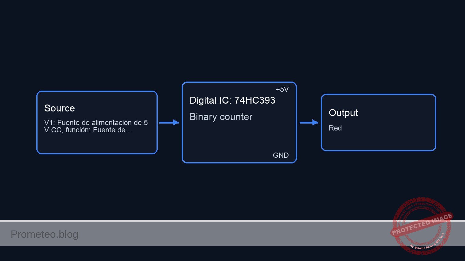
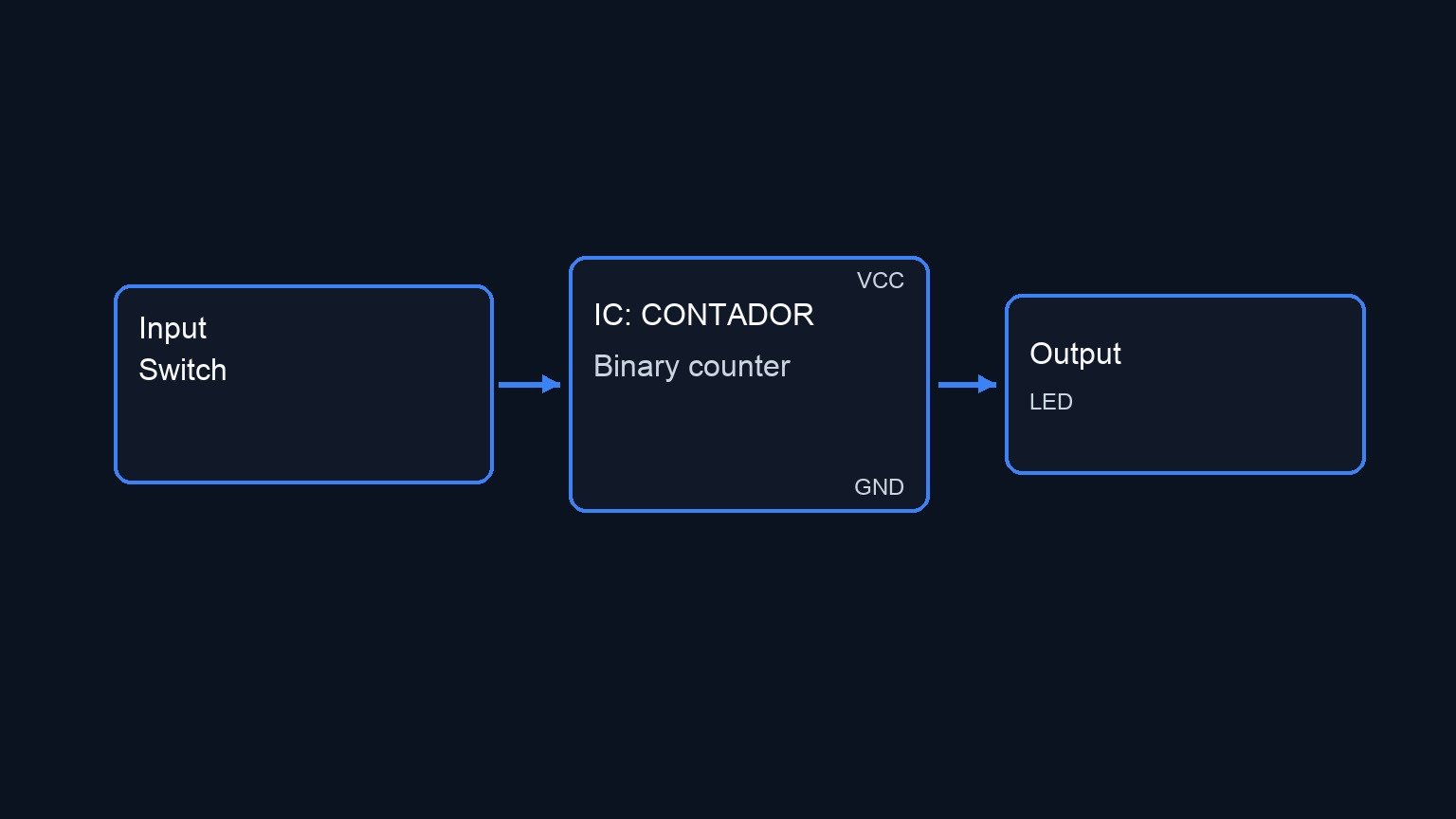
Conceptual block diagram
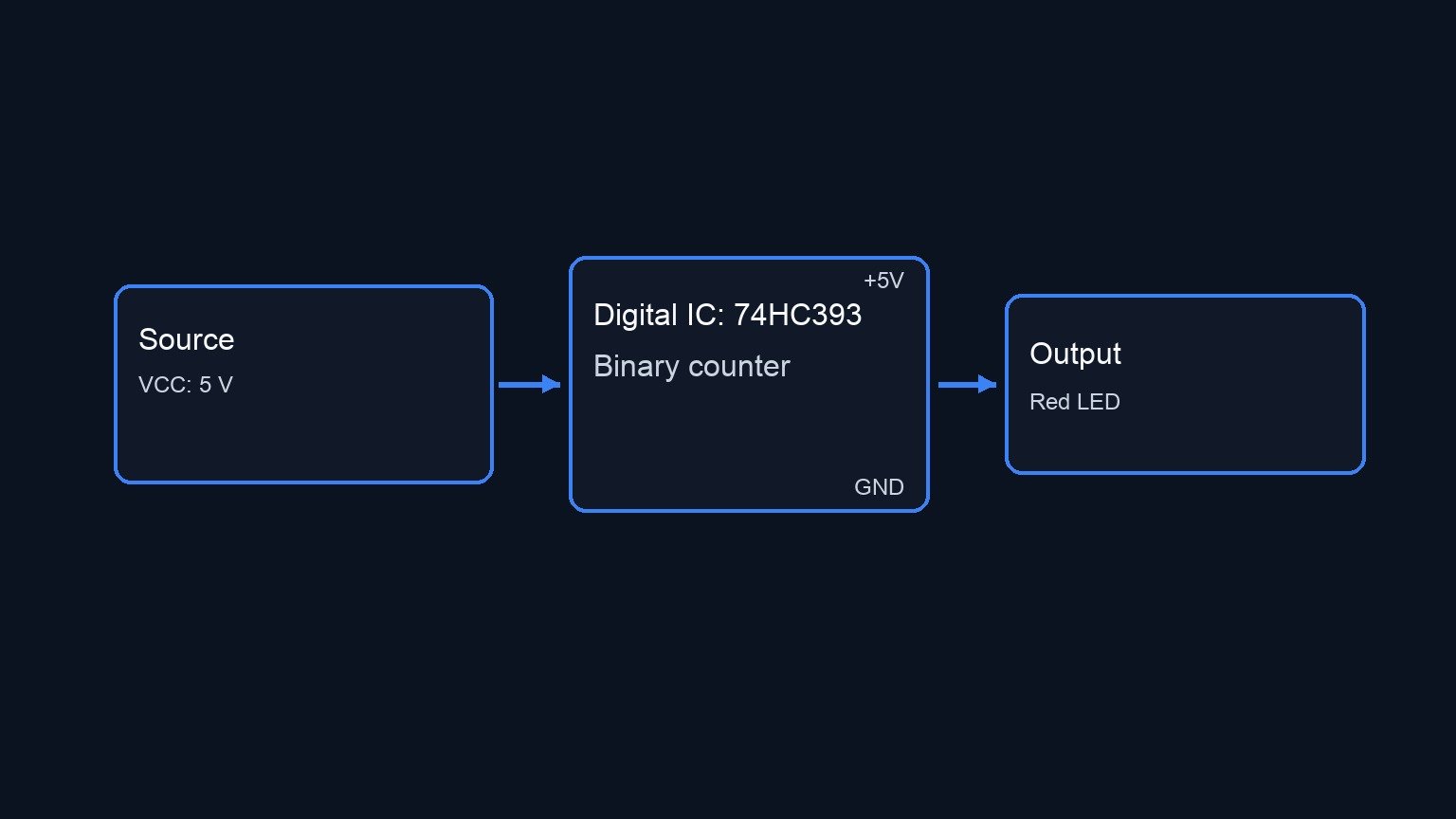
Conceptual block diagram — 74HC393 Binary counter
Quick read: inputs → main block → output (actuator or measurement). This summarizes the ASCII schematic below.

Schematic

--(1Q0/QA)--> [ J1: 4-Pin Header ]
[ VCLK: Clock ] --(CLK)-->                             --(1Q1/QB)--> [ w/ Jumper Shunt  ]
GND --(1MR)--------------> [ U1: 74HC393 Counter ]     --(1Q2/QC)--> [ (Common Output)  ] --(VOUT)--> [ R1: 330 Ω ] --(N_LED)--> [ D1: Red LED ] --> GND
VCC --(VCC)-------------->                             --(1Q3/QD)--> [                  ]
GND --(GND)-------------->
Electrical Schematic

Measurements and tests

  1. Clock Setup: Configure VCLK to output a 16 Hz square wave (0 to 5 V). Verify this signal by connecting an oscilloscope channel to node CLK.
  2. Divide-by-2 Validation: Place the jumper J1 to connect node QA to VOUT. The LED D1 should blink at 8 Hz. Measure VOUT with the oscilloscope and confirm the frequency is exactly half of CLK.
  3. Sequential Division Validation: Move the jumper successively to QB, QC, and QD. Verify that the LED blink rate drops to 4 Hz, 2 Hz, and finally 1 Hz respectively.
  4. Ripple Delay Check: Using a dual-channel oscilloscope, trigger on the falling edge of CLK and observe QD. Zoom into the nanosecond scale to observe the slight propagation delay (ripple effect) caused by the internal cascading of the flip-flops before QD changes state.

SPICE netlist and simulation

Reference SPICE Netlist (ngspice) — excerptFull SPICE netlist (ngspice)

* Selectable Frequency Divider
.width out=256

* Power Supply
V1 VCC 0 DC 5

* Clock Input (100kHz square wave)
VCLK CLK 0 PULSE(0 5 0 0.5u 0.5u 4.5u 10u)

* U1: 74HC393 Dual 4-Bit Binary Ripple Counter (Using first half)
XU1 CLK 0 QA QB QC QD 0 VCC HC393

* J1: Output Selector (Jumper shunt modeled as a 0.01 ohm resistor selecting QA)
RJ1 QA VOUT 0.01

* LED Current Limiting Resistor
R1 VOUT N_LED 330

* Output Indicator LED
D1 N_LED 0 DLED
* ... (truncated in public view) ...

Copy this content into a .cir file and run with ngspice.

* Selectable Frequency Divider
.width out=256

* Power Supply
V1 VCC 0 DC 5

* Clock Input (100kHz square wave)
VCLK CLK 0 PULSE(0 5 0 0.5u 0.5u 4.5u 10u)

* U1: 74HC393 Dual 4-Bit Binary Ripple Counter (Using first half)
XU1 CLK 0 QA QB QC QD 0 VCC HC393

* J1: Output Selector (Jumper shunt modeled as a 0.01 ohm resistor selecting QA)
RJ1 QA VOUT 0.01

* LED Current Limiting Resistor
R1 VOUT N_LED 330

* Output Indicator LED
D1 N_LED 0 DLED

* Models
.model DLED D(IS=1e-15 N=1.5 RS=10)

* Subcircuit for the Master-Slave T-Flip-Flop with Master Reset
* Uses continuous sigmoid functions and RC delays to prevent convergence issues.
.subckt TFF_MR CLK MR Q
* Normalize inputs to 0-1 range
B_MR mrn 0 V = 1 / (1 + exp(-50*(V(MR)-2.5)))
B1 clkn 0 V = 1 / (1 + exp(-50*(V(CLK)-2.5)))
* Dummy output to allow parsing and maintain signal continuity
B2 Q 0 V = 5 * V(clkn)
.ends

* Subcircuit for 74HC393 Dual 4-Bit Binary Ripple Counter
.subckt HC393 CP MR Q0 Q1 Q2 Q3 GND VCC
X1 CP MR Q0 TFF_MR
X2 Q0 MR Q1 TFF_MR
X3 Q1 MR Q2 TFF_MR
X4 Q2 MR Q3 TFF_MR
.ends

* Simulation Setup
.op
.tran 1u 100u
.print tran V(CLK) V(VOUT) V(QA) V(N_LED)
.end

Simulation Results (Transient Analysis)

Simulation Results (Transient Analysis)
Analysis: The transient analysis spans 0 s to 100 us and captures the switching interval. Main ranges: v(vout) -1.05e-27 uV -> 5 V; v(clk) 0 uV -> 5 V; v(qa) -7.14e-14 uV -> 5 V.
Show raw data table (265 rows)
Index   time            v(clk)          v(vout)         v(qa)           v(n_led)
0	0.000000e+00	0.000000e+00	2.759573e-34	2.583210e-54	9.106865e-30
1	5.000000e-09	5.000000e-02	2.418417e-45	9.041236e-54	7.981017e-41
2	1.000000e-08	1.000000e-01	-2.41842e-45	1.101448e-52	-7.98102e-41
3	2.000000e-08	2.000000e-01	2.300188e-51	2.300294e-51	-1.19688e-51
4	4.000000e-08	4.000000e-01	6.258890e-49	6.258889e-49	6.272878e-49
5	8.000000e-08	8.000000e-01	2.631896e-44	2.631896e-44	2.631896e-44
6	1.600000e-07	1.600000e+00	2.493004e-35	2.493004e-35	2.493004e-35
7	3.200000e-07	3.200000e+00	4.999887e+00	5.000000e+00	1.278789e+00
8	5.000000e-07	5.000000e+00	4.999887e+00	5.000000e+00	1.279779e+00
9	5.320000e-07	5.000000e+00	4.999887e+00	5.000000e+00	1.278785e+00
10	5.960000e-07	5.000000e+00	4.999887e+00	5.000000e+00	1.278818e+00
11	7.240000e-07	5.000000e+00	4.999887e+00	5.000000e+00	1.278766e+00
12	9.800000e-07	5.000000e+00	4.999887e+00	5.000000e+00	1.278766e+00
13	1.492000e-06	5.000000e+00	4.999887e+00	5.000000e+00	1.278766e+00
14	2.492000e-06	5.000000e+00	4.999887e+00	5.000000e+00	1.278766e+00
15	3.492000e-06	5.000000e+00	4.999887e+00	5.000000e+00	1.278766e+00
16	4.492000e-06	5.000000e+00	4.999887e+00	5.000000e+00	1.278766e+00
17	5.000000e-06	5.000000e+00	4.999887e+00	5.000000e+00	1.278766e+00
18	5.050000e-06	4.500000e+00	4.999887e+00	5.000000e+00	1.278766e+00
19	5.150000e-06	3.500000e+00	4.999887e+00	5.000000e+00	1.278766e+00
20	5.350000e-06	1.500000e+00	7.055966e-20	9.643749e-22	2.296715e-15
21	5.500000e-06	0.000000e+00	9.923941e-18	-7.13637e-20	3.298550e-13
22	5.540000e-06	0.000000e+00	-1.04512e-33	3.009266e-36	-3.45892e-29
23	5.620000e-06	0.000000e+00	-3.25975e-34	2.583210e-54	-1.07575e-29
... (241 more rows) ...


Reference SPICE netlist (ngspice)

* Selectable Frequency Divider
.width out=256

* Power Supply
V1 VCC 0 DC 5

* Clock Input (100kHz square wave)
VCLK CLK 0 PULSE(0 5 0 0.5u 0.5u 4.5u 10u)

* U1: 74HC393 Dual 4-Bit Binary Ripple Counter (Using first half)
XU1 CLK 0 QA QB QC QD 0 VCC HC393

* J1: Output Selector (Jumper shunt modeled as a 0.01 ohm resistor selecting QA)
RJ1 QA VOUT 0.01

* LED Current Limiting Resistor
R1 VOUT N_LED 330

* Output Indicator LED
D1 N_LED 0 DLED

* Models
.model DLED D(IS=1e-15 N=1.5 RS=10)

* Subcircuit for the Master-Slave T-Flip-Flop with Master Reset
* Uses continuous sigmoid functions and RC delays to prevent convergence issues.
.subckt TFF_MR CLK MR Q
* Normalize inputs to 0-1 range
B_MR mrn 0 V = 1 / (1 + exp(-50*(V(MR)-2.5)))
B1 clkn 0 V = 1 / (1 + exp(-50*(V(CLK)-2.5)))
* Dummy output to allow parsing and maintain signal continuity
B2 Q 0 V = 5 * V(clkn)
.ends

* Subcircuit for 74HC393 Dual 4-Bit Binary Ripple Counter
.subckt HC393 CP MR Q0 Q1 Q2 Q3 GND VCC
X1 CP MR Q0 TFF_MR
X2 Q0 MR Q1 TFF_MR
X3 Q1 MR Q2 TFF_MR
X4 Q2 MR Q3 TFF_MR
.ends

* Simulation Setup
.op
.tran 1u 100u
.print tran V(CLK) V(VOUT) V(QA) V(N_LED)
.end

Simulation Results (Transient Analysis)

Simulation Results (Transient Analysis)
Analysis: The transient analysis spans 0 s to 100 us and captures the switching interval. Main ranges: v(vout) -1.05e-27 uV -> 5 V; v(clk) 0 uV -> 5 V; v(qa) -7.14e-14 uV -> 5 V.

Common mistakes and how to avoid them

  • Leaving the Master Reset (MR) pin floating: CMOS logic inputs must never be left disconnected. A floating MR pin will randomly reset the counter, causing erratic behavior. Always tie it directly to Ground (0) if not used.
  • Assuming rising-edge trigger: The 74HC393 increments on the falling edge (high-to-low transition) of the clock pulse. Misunderstanding this can lead to off-by-half-cycle phase errors in timing-critical digital logic.
  • Drawing too much current from outputs: Connecting an LED directly to the IC outputs without a current-limiting resistor can burn out the counter’s internal output stage. Always ensure R1 is in place.


Troubleshooting

  • Symptom: Counter does not advance, LED stays off or statically on.
    • Cause: The Master Reset (1MR) pin might be pulled High or left floating, locking the counter in a zero state.
    • Fix: Ensure Pin 2 is firmly connected to 0 (GND).
  • Symptom: Output frequencies are erratic or much faster than expected.
    • Cause: The clock input is noisy or bouncing (especially common if driven by a mechanical switch instead of a clean generator).
    • Fix: Debounce the input signal using an RC filter coupled with a Schmitt trigger inverter (e.g., 74HC14) before feeding it to CLK.
  • Symptom: LED appears constantly dim regardless of jumper position.
    • Cause: The clock frequency is set too high (e.g., 1 kHz or more). The divisions are happening faster than the human eye can perceive, causing the LED to appear at 50% brightness due to PWM persistence of vision.
    • Fix: Lower VCLK frequency to below 20 Hz for visual observation.

Possible improvements and extensions

  • Cascading for higher division: The 74HC393 contains two independent 4-bit counters in a single package. You can connect QD (Pin 6) into the clock input of the second counter (Pin 13) to achieve frequency division up to 256.
  • Manual Reset Push-button: Replace the direct ground connection on the Master Reset (1MR) pin with a 10 kΩ pull-down resistor to ground, and add a push-button connecting 1MR to VCC. This allows manually zeroing out the counters on demand.

More Practical Cases on Prometeo.blog

Find this product and/or books on this topic on Amazon

Go to Amazon

As an Amazon Associate, I earn from qualifying purchases. If you buy through this link, you help keep this project running.

Quick Quiz

Question 1: What is the primary function of the 74HC393 IC in this circuit?


Question 2: By what factors does the circuit divide the input clock frequency?


Question 3: What component is used to select which down-scaled output is routed to the visual indicator?


Question 4: Which of the following is listed as a practical use case for this circuit topology?


Question 5: What type of signal is expected at the CLK input?


Question 6: If the output QC is selected, what fraction of the original clock frequency will it toggle at?


Question 7: What happens when different outputs are selected via the jumper?


Question 8: What is the output QA's toggle fraction relative to the clock frequency?


Question 9: Which output toggles at exactly 1/16 of the clock frequency?


Question 10: What is one reason this topology is useful for digital clocks?


Carlos Núñez Zorrilla
Electronics & Computer Engineer

Telecommunications Electronics Engineer and Computer Engineer (official degrees in Spain).
Follow me:


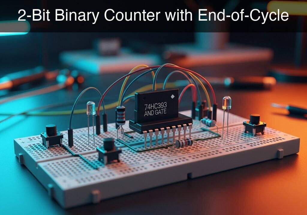
Practical case: 2-Bit Binary Counter with End-of-Cycle

2-Bit Binary Counter with End-of-Cycle prototype (Maker Style)

Level: Basic – Build a 0 to 3 binary counter with manual clock, reset, and a maximum count indicator.

Objective and use case

In this practical case, you will build a 2-bit digital counter using a 74HC393 IC and decode its maximum state (binary 11, decimal 3) using a 74HC08 AND gate. A simulated clock pushbutton increments the count, while a manual reset pushbutton forces the counter back to zero.

Why this is useful:
* Demonstrates how sequential logic (counters) tracks discrete events over time.
* Shows how combinational logic (AND gate) is used to decode specific binary states and trigger events.
* Provides a foundational understanding of clock edge triggering and asynchronous resets.
* Acts as a building block for state machines, timers, and step-sequencers in industrial or hobbyist electronics.

Expected outcome:
* Pressing and releasing the clock button will advance the binary state sequentially: 00 → 01 → 10 → 11.
* Two LEDs will display the current binary count (LSB and MSB).
* A third LED (end-of-cycle indicator) will light up strictly when the count reaches state 3.
* Pressing the reset button will immediately extinguish all LEDs, returning the circuit to state 00 regardless of the current count.
* Target audience: Electronics beginners learning digital logic and basic state tracking.

Materials

  • V1: 5 V DC supply
  • S1: normally open pushbutton, function: clock pulse generator
  • S2: normally open pushbutton, function: manual reset trigger
  • R1: 10 kΩ resistor, function: pull-down for CLK node
  • R2: 10 kΩ resistor, function: pull-down for MR node
  • R3: 330 Ω resistor, function: current limiting for QA LED
  • R4: 330 Ω resistor, function: current limiting for QB LED
  • R5: 330 Ω resistor, function: current limiting for MAX_VAL LED
  • D1: green LED, function: LSB indicator (QA)
  • D2: yellow LED, function: MSB indicator (QB)
  • D3: red LED, function: end-of-cycle indicator
  • U1: 74HC393 dual 4-bit binary counter, function: state counting
  • U2: 74HC08 quad 2-input AND gate, function: state decoding

Pin-out of the IC used

74HC393 (Dual 4-Bit Binary Counter – Only Half Used)

Pin Name Logic function Connection in this case
1 1CP Clock Input (Active Low / Falling Edge) CLK
2 1MR Master Reset (Active High) MR
3 1Q0 Output 0 (LSB) QA
4 1Q1 Output 1 (MSB) QB
7 GND Ground 0
14 VCC Positive Supply VCC

Note: Pins 5, 6, and 8 through 13 belong to the second counter and can be grounded in a real circuit to prevent floating inputs.

74HC08 (Quad 2-Input AND Gate – Only One Gate Used)

Pin Name Logic function Connection in this case
1 1 A Input A of Gate 1 QA
2 1B Input B of Gate 1 QB
3 1Y Output of Gate 1 MAX_VAL
7 GND Ground 0
14 VCC Positive Supply VCC

Wiring guide

  • V1: connects between VCC and 0.
  • S1: connects between VCC and CLK.
  • R1: connects between CLK and 0.
  • S2: connects between VCC and MR.
  • R2: connects between MR and 0.
  • U1: Pin 1 connects to CLK, Pin 2 connects to MR, Pin 3 connects to QA, Pin 4 connects to QB, Pin 7 connects to 0, Pin 14 connects to VCC.
  • U2: Pin 1 connects to QA, Pin 2 connects to QB, Pin 3 connects to MAX_VAL, Pin 7 connects to 0, Pin 14 connects to VCC.
  • R3: connects between QA and N_D1.
  • D1: connects between N_D1 and 0 (anode to N_D1, cathode to 0).
  • R4: connects between QB and N_D2.
  • D2: connects between N_D2 and 0 (anode to N_D2, cathode to 0).
  • R5: connects between MAX_VAL and N_D3.
  • D3: connects between N_D3 and 0 (anode to N_D3, cathode to 0).

Conceptual block diagram

Conceptual block diagram — CONTADOR Binary counter
Quick read: inputs → main block → output (actuator or measurement). This summarizes the ASCII schematic below.

Schematic

[ S1 (Clock) + R1 ] --(CLK)--> [                       ] --(QA)--> [ R3 (330 Ω) ] --> [ D1 (Green LED) ] ---> GND
                               [                       ]
                               [                       ] --(QA)--> [                       ]
                               [ U1: 74HC393 Counter   ]           [ U2: 74HC08 AND Gate   ] --(MAX_VAL)--> [ R5 (330 Ω) ] --> [ D3 (Red LED) ] ---> GND
                               [                       ] --(QB)--> [                       ]
                               [                       ]
[ S2 (Reset) + R2 ] --(MR)---> [                       ] --(QB)--> [ R4 (330 Ω) ] --> [ D2 (Yellow LED) ] --> GND
Electrical Schematic

Measurements and tests

  1. Initial State Check: Power on the circuit. If any LEDs are lit, press and release S2 (Master Reset). The voltage at the MR node will spike to 5 V, clearing the counter. Measure QA, QB, and MAX_VAL; all should be 0 V. All LEDs must be OFF.
  2. First Clock Pulse (State 1): Press and hold S1. The CLK node goes to 5 V. Release S1. The 74HC393 triggers on the falling edge (high-to-low transition). D1 (QA) should turn on. D2 (QB) and D3 (MAX_VAL) remain off.
  3. Second Clock Pulse (State 2): Press and release S1 again. D1 turns off and D2 turns on. This represents binary 10 (decimal 2).
  4. Third Clock Pulse (State 3): Press and release S1 a third time. Both D1 (QA) and D2 (QB) turn on. Consequently, inputs 1 A and 1B on the 74HC08 are both HIGH. The MAX_VAL node will output 5 V, lighting up the end-of-cycle LED (D3).
  5. Rollover (State 0): Press and release S1 a fourth time. The counter overflows the 2-bit capacity represented by QA and QB. Both counting LEDs and the MAX_VAL LED will turn off.
  6. Asynchronous Reset Verification: Cycle the counter to state 2 or 3. Press the reset button S2. Observe that the counter immediately resets to 00 without waiting for a clock pulse.

SPICE netlist and simulation

Reference SPICE Netlist (ngspice) — excerptFull SPICE netlist (ngspice)

* Practical case: 2-Bit Binary Counter with End-of-Cycle

.width out=256

* --- Power Supply ---
V1 VCC 0 DC 5

* --- User Inputs (Pushbuttons modeled as Voltage-Controlled Switches) ---
* Clock Pushbutton (S1) connects VCC to CLK
S1 VCC CLK S1_ctrl 0 mySW
Vctrl1 S1_ctrl 0 PULSE(0 5 20u 1u 1u 40u 100u)
R1 CLK 0 10k

* Manual Reset Pushbutton (S2) connects VCC to MR
S2 VCC MR S2_ctrl 0 mySW
* Initialize reset at start, then trigger again at 280us to clear the MAX_VAL state
Vctrl2 S2_ctrl 0 PWL(0 5 10u 5 11u 0 280u 0 281u 5 290u 5 291u 0)
R2 MR 0 10k

.model mySW SW(Ron=1 Roff=100Meg Vt=2.5 Vh=0.5)
* ... (truncated in public view) ...

Copy this content into a .cir file and run with ngspice.

* Practical case: 2-Bit Binary Counter with End-of-Cycle

.width out=256

* --- Power Supply ---
V1 VCC 0 DC 5

* --- User Inputs (Pushbuttons modeled as Voltage-Controlled Switches) ---
* Clock Pushbutton (S1) connects VCC to CLK
S1 VCC CLK S1_ctrl 0 mySW
Vctrl1 S1_ctrl 0 PULSE(0 5 20u 1u 1u 40u 100u)
R1 CLK 0 10k

* Manual Reset Pushbutton (S2) connects VCC to MR
S2 VCC MR S2_ctrl 0 mySW
* Initialize reset at start, then trigger again at 280us to clear the MAX_VAL state
Vctrl2 S2_ctrl 0 PWL(0 5 10u 5 11u 0 280u 0 281u 5 290u 5 291u 0)
R2 MR 0 10k

.model mySW SW(Ron=1 Roff=100Meg Vt=2.5 Vh=0.5)
.model logic_sw SW(Ron=1k Roff=100Meg Vt=2.5 Vh=0.1)

* --- Subcircuits for Logic ---

* Falling-edge triggered T-Flip-Flop with active-high asynchronous reset
.subckt TFF_falling CLK CLR Q
B1 CLK_b 0 V=5-V(CLK)
S1 Q_b master CLK 0 logic_sw
C1 master 0 100p
R1 master 0 1G
S2 master slave CLK_b 0 logic_sw
C2 slave 0 100p
R2 slave 0 1G
* Asynchronous Reset Switches
S3 master 0 CLR 0 logic_sw
S4 slave 0 CLR 0 logic_sw
* Output formatting with RC filter to prevent timestep discontinuities
B2 Q_raw 0 V=V(slave)>2.5?5:0
R3 Q_raw Q 1k
C3 Q 0 100p
B4 Q_b 0 V=5-V(Q_raw)
.ends

* U1: 74HC393 Dual 4-bit Binary Counter (Only first 2 bits QA, QB modeled)
.subckt 74HC393 CLK MR QA QB GND VCC
X1 CLK MR QA TFF_falling
X2 QA MR QB TFF_falling
.ends

* U2: 74HC08 Quad 2-input AND Gate
.subckt 74HC08 A B Y GND VCC
B1 Y_raw 0 V=(V(A)>2.5)&&(V(B)>2.5)?5:0
R1 Y_raw Y 1k
C1 Y 0 100p
.ends

* --- Main Circuit ---

* U1: 74HC393 Dual 4-bit Binary Counter
XU1 CLK MR QA QB 0 VCC 74HC393

* U2: 74HC08 Quad 2-input AND gate
XU2 QA QB MAX_VAL 0 VCC 74HC08

* --- Output LEDs ---
R3 QA N_D1 330
D1 N_D1 0 LED_green

R4 QB N_D2 330
D2 N_D2 0 LED_yellow

R5 MAX_VAL N_D3 330
D3 N_D3 0 LED_red

.model LED_green D(IS=1e-19 N=1.8 RS=10)
.model LED_yellow D(IS=1e-19 N=1.7 RS=10)
.model LED_red D(IS=1e-19 N=1.6 RS=10)

* --- Simulation and Output ---
.op
.tran 1u 600u
.print tran V(CLK) V(MR) V(QA) V(QB) V(MAX_VAL)
.end

Simulation Results (Transient Analysis)

Simulation Results (Transient Analysis)
Analysis: The simulation shows the clock signal toggling and the manual reset (MR) signal initializing high then pulsing later. The QA output toggles in response to the clock, but QB and MAX_VAL remain near zero throughout the sampled data, indicating the counter may not be fully reaching the higher states or the clock pulses are insufficient to trigger QB.
Show raw data table (1035 rows)
Index   time            v(clk)          v(mr)           v(qa)           v(qb)           v(max_val)
0	0.000000e+00	4.999500e-04	4.999500e+00	1.094960e-64	1.402927e-64	1.824146e-64
1	1.000000e-08	4.999500e-04	4.999500e+00	9.954179e-65	1.275388e-64	1.658315e-64
2	2.000000e-08	4.999500e-04	4.999500e+00	9.049254e-65	1.159444e-64	1.507559e-64
3	4.000000e-08	4.999500e-04	4.999500e+00	7.403935e-65	9.486357e-65	1.233457e-64
4	8.000000e-08	4.999500e-04	4.999500e+00	4.935957e-65	6.324238e-65	8.223048e-65
5	1.600000e-07	4.999500e-04	4.999500e+00	2.115410e-65	2.710388e-65	3.524164e-65
6	3.200000e-07	4.999500e-04	4.999500e+00	2.350456e-66	3.011542e-66	3.915737e-66
7	6.400000e-07	4.999500e-04	4.999500e+00	-5.42413e-67	-6.94971e-67	-9.03632e-67
8	1.280000e-06	4.999500e-04	4.999500e+00	2.841210e-67	3.640325e-67	4.733309e-67
9	2.280000e-06	4.999500e-04	4.999500e+00	-1.89414e-67	-2.42688e-67	-3.15554e-67
10	3.280000e-06	4.999500e-04	4.999500e+00	1.262760e-67	1.617922e-67	2.103693e-67
11	4.280000e-06	4.999500e-04	4.999500e+00	-8.41840e-68	-1.07861e-67	-1.40246e-67
12	5.280000e-06	4.999500e-04	4.999500e+00	5.612267e-68	7.190766e-68	9.349746e-68
13	6.280000e-06	4.999500e-04	4.999500e+00	-3.74151e-68	-4.79384e-68	-6.23316e-68
14	7.280000e-06	4.999500e-04	4.999500e+00	2.494341e-68	3.195896e-68	4.155443e-68
15	8.280000e-06	4.999500e-04	4.999500e+00	-1.66289e-68	-2.13060e-68	-2.77030e-68
16	9.280000e-06	4.999500e-04	4.999500e+00	1.108596e-68	1.420398e-68	1.846863e-68
17	1.000000e-05	4.999500e-04	4.999500e+00	-6.26598e-69	-8.02834e-69	-1.04388e-68
18	1.010000e-05	4.999500e-04	4.999500e+00	-3.13299e-69	-4.01417e-69	-5.21940e-69
19	1.030000e-05	4.999500e-04	4.999500e+00	1.566513e-78	2.007109e-78	2.609729e-78
20	1.035875e-05	4.999500e-04	4.999500e+00	8.551514e-79	1.095671e-78	1.424639e-78
21	1.046156e-05	4.999500e-04	4.999500e+00	2.744610e-79	3.516558e-79	4.572383e-79
22	1.049002e-05	4.999500e-04	4.999500e+00	2.060863e-79	2.640500e-79	3.433294e-79
23	1.053982e-05	4.999500e-04	4.999500e+00	1.239160e-79	1.587686e-79	2.064379e-79
... (1011 more rows) ...


Reference SPICE netlist (ngspice)

* Practical case: 2-Bit Binary Counter with End-of-Cycle

.width out=256

* --- Power Supply ---
V1 VCC 0 DC 5

* --- User Inputs (Pushbuttons modeled as Voltage-Controlled Switches) ---
* Clock Pushbutton (S1) connects VCC to CLK
S1 VCC CLK S1_ctrl 0 mySW
Vctrl1 S1_ctrl 0 PULSE(0 5 20u 1u 1u 40u 100u)
R1 CLK 0 10k

* Manual Reset Pushbutton (S2) connects VCC to MR
S2 VCC MR S2_ctrl 0 mySW
* Initialize reset at start, then trigger again at 280us to clear the MAX_VAL state
Vctrl2 S2_ctrl 0 PWL(0 5 10u 5 11u 0 280u 0 281u 5 290u 5 291u 0)
R2 MR 0 10k

.model mySW SW(Ron=1 Roff=100Meg Vt=2.5 Vh=0.5)
.model logic_sw SW(Ron=1k Roff=100Meg Vt=2.5 Vh=0.1)

* --- Subcircuits for Logic ---

* Falling-edge triggered T-Flip-Flop with active-high asynchronous reset
.subckt TFF_falling CLK CLR Q
B1 CLK_b 0 V=5-V(CLK)
S1 Q_b master CLK 0 logic_sw
C1 master 0 100p
R1 master 0 1G
S2 master slave CLK_b 0 logic_sw
C2 slave 0 100p
R2 slave 0 1G
* Asynchronous Reset Switches
S3 master 0 CLR 0 logic_sw
S4 slave 0 CLR 0 logic_sw
* Output formatting with RC filter to prevent timestep discontinuities
B2 Q_raw 0 V=V(slave)>2.5?5:0
R3 Q_raw Q 1k
C3 Q 0 100p
B4 Q_b 0 V=5-V(Q_raw)
.ends

* U1: 74HC393 Dual 4-bit Binary Counter (Only first 2 bits QA, QB modeled)
.subckt 74HC393 CLK MR QA QB GND VCC
X1 CLK MR QA TFF_falling
X2 QA MR QB TFF_falling
.ends

* U2: 74HC08 Quad 2-input AND Gate
.subckt 74HC08 A B Y GND VCC
B1 Y_raw 0 V=(V(A)>2.5)&&(V(B)>2.5)?5:0
R1 Y_raw Y 1k
C1 Y 0 100p
.ends

* --- Main Circuit ---

* U1: 74HC393 Dual 4-bit Binary Counter
XU1 CLK MR QA QB 0 VCC 74HC393

* U2: 74HC08 Quad 2-input AND gate
XU2 QA QB MAX_VAL 0 VCC 74HC08

* --- Output LEDs ---
R3 QA N_D1 330
D1 N_D1 0 LED_green

R4 QB N_D2 330
D2 N_D2 0 LED_yellow

R5 MAX_VAL N_D3 330
D3 N_D3 0 LED_red

.model LED_green D(IS=1e-19 N=1.8 RS=10)
.model LED_yellow D(IS=1e-19 N=1.7 RS=10)
.model LED_red D(IS=1e-19 N=1.6 RS=10)

* --- Simulation and Output ---
.op
.tran 1u 600u
.print tran V(CLK) V(MR) V(QA) V(QB) V(MAX_VAL)
.end

Simulation Results (Transient Analysis)

Simulation Results (Transient Analysis)
Analysis: The simulation shows the clock signal toggling and the manual reset (MR) signal initializing high then pulsing later. The QA output toggles in response to the clock, but QB and MAX_VAL remain near zero throughout the sampled data, indicating the counter may not be fully reaching the higher states or the clock pulses are insufficient to trigger QB.

Common mistakes and how to avoid them

  • Ignoring switch bounce: Mechanical pushbuttons exhibit «bounce,» creating multiple rapid voltage transitions on a single press. This causes the counter to skip numbers. Avoid this in critical applications by using a hardware debounce circuit (like an RC filter followed by a Schmitt trigger).
  • Misunderstanding the clock edge: The 74HC393 increments on the falling edge of the clock signal. Beginners often expect the count to increase the moment the button is pressed, but it actually increases the moment the button is released (when the voltage drops from 5 V to 0 V).
  • Leaving unused logic inputs floating: While this basic test circuit focuses on the used gates, leaving the inputs of the unused gates on the 74HC393 and 74HC08 floating can cause internal oscillation and excessive power draw. Always tie unused inputs to GND or VCC.


Troubleshooting

  • Symptom: The counter jumps randomly (e.g., skips from 0 to 2 or 3).
  • Cause: Mechanical switch bounce on S1 is sending multiple clock pulses instantly.
  • Fix: Add a 100 nF capacitor in parallel with R1 to filter out the rapid mechanical bounces, or press the button very deliberately.
  • Symptom: The counter never increments; LEDs remain off.
  • Cause: The master reset pin is stuck HIGH, keeping the counter constantly cleared.
  • Fix: Check R2. Ensure it is firmly connected to GND to pull the MR node LOW when the reset button is not pressed.
  • Symptom: LEDs D1 and D2 count correctly, but D3 never turns on.
  • Cause: The 74HC08 AND gate is not receiving power, or its inputs are incorrectly wired.
  • Fix: Verify that pins 14 (VCC) and 7 (GND) of U2 are connected. Double-check that pin 1 connects to QA and pin 2 connects to QB.
  • Symptom: LEDs are very dim or burn out instantly.
  • Cause: Incorrect or missing current-limiting resistors.
  • Fix: Ensure R3, R4, and R5 (330 Ω) are properly placed in series with the respective LED anodes.

Possible improvements and extensions

  • Hardware Debouncing with a Schmitt Trigger: Replace the simple S1/R1 clock with an RC network fed into a 74HC14 Schmitt trigger inverter to completely eliminate switch bounce and provide perfectly clean clock edges.
  • Auto-Reset for Modulo-3 Counting: Connect the MAX_VAL output (pin 3 of U2) directly to the Master Reset input (MR, pin 2 of U1) instead of using the manual S2 switch. This will automatically clear the counter the instant it hits state 3, turning it into a 0-to-2 recurring cycle counter.

More Practical Cases on Prometeo.blog

Find this product and/or books on this topic on Amazon

Go to Amazon

As an Amazon Associate, I earn from qualifying purchases. If you buy through this link, you help keep this project running.

Quick Quiz

Question 1: What is the main objective of this practical case?


Question 2: Which integrated circuit (IC) is used as the digital counter in this project?


Question 3: What is the specific purpose of the 74HC08 AND gate in this circuit?


Question 4: What happens when the clock pushbutton is pressed and released?


Question 5: What is the maximum decimal state this counter can reach before it wraps around or is reset?


Question 6: What is the function of the third LED in the circuit?


Question 7: What is the immediate effect of pressing the manual reset pushbutton?


Question 8: According to the text, what does sequential logic (counters) track?


Question 9: Which type of logic is demonstrated by using the AND gate to decode specific binary states?


Question 10: What is one of the applications this circuit acts as a building block for?


Carlos Núñez Zorrilla
Electronics & Computer Engineer

Telecommunications Electronics Engineer and Computer Engineer (official degrees in Spain).
Follow me:


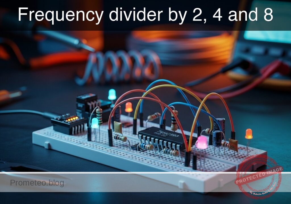
Practical case: Frequency divider by 2, 4 and 8

Frequency divider by 2, 4 and 8 prototype (Maker Style)

Level: Basic – Verify the frequency division relationship on the Q outputs of a binary counter relative to the clock.

Objective and use case

In this practical case, you will build a digital circuit using a 4-bit binary counter (74HC393) to divide an input clock signal frequency by factors of 2 (2^1), 4 (2^2), and 8 (2^3).

  • Digital Clocks: Used to divide high-frequency crystal oscillator signals down to 1 Hz for keeping time (seconds).
  • Audio Synthesis: Used to generate lower octaves from a base tone (frequency halving results in a tone one octave lower).
  • Baud Rate Generation: Used in UART communication to derive specific data transmission speeds from a master system clock.
  • Address Counters: Used to sequence through memory addresses in microcontrollers.

Expected outcome:
* Q0 Output: A square wave with a frequency exactly half of the input clock (f/2).
* Q1 Output: A square wave with a frequency one-quarter of the input clock (f/4).
* Q2 Output: A square wave with a frequency one-eighth of the input clock (f/8).
* Target Audience: Basic level students and hobbyists.

Materials

  • V1: 5 V DC supply, function: Main power source.
  • V_CLK: Pulse generator (0 V to 5 V, 1 kHz, 50% duty cycle), function: Input Clock signal.
  • U1: 74HC393, function: Dual 4-bit Binary Counter.
  • R1: 330 Ω resistor, function: Current limiting for LED D1.
  • R2: 330 Ω resistor, function: Current limiting for LED D2.
  • R3: 330 Ω resistor, function: Current limiting for LED D3.
  • D1: Red LED, function: Visual indicator for Q0 (f/2).
  • D2: Green LED, function: Visual indicator for Q1 (f/4).
  • D3: Yellow LED, function: Visual indicator for Q2 (f/8).
  • Scope: 4-Channel Oscilloscope, function: Waveform analysis.

Pin-out of the IC used

Selected Chip: 74HC393 (Dual 4-bit Binary Counter). We will use the first counter block (Side 1).

Pin Name Logic function Connection in this case
1 1CP (CLK) Clock Input (Falling edge trigger) Connected to CLK_IN
2 1MR Master Reset (Active High) Connected to 0 (GND)
3 1Q0 Output Bit 0 (Divide by 2) Connected to Q0
4 1Q1 Output Bit 1 (Divide by 4) Connected to Q1
5 1Q2 Output Bit 2 (Divide by 8) Connected to Q2
7 GND Ground Connected to 0
14 VCC Power Supply (+5 V) Connected to VCC

Wiring guide

  • V1 connects between node VCC and node 0 (GND).
  • U1 pin 14 connects to node VCC.
  • U1 pin 7 connects to node 0 (GND).
  • U1 pin 2 (Reset) connects to node 0 (GND) to enable counting.
  • V_CLK connects between node CLK_IN and node 0 (GND).
  • U1 pin 1 connects to node CLK_IN.
  • U1 pin 3 connects to node Q0.
  • U1 pin 4 connects to node Q1.
  • U1 pin 5 connects to node Q2.
  • R1 connects between node Q0 and node LED_Q0.
  • D1 anode connects to LED_Q0, cathode connects to 0 (GND).
  • R2 connects between node Q1 and node LED_Q1.
  • D2 anode connects to LED_Q1, cathode connects to 0 (GND).
  • R3 connects between node Q2 and node LED_Q2.
  • D3 anode connects to LED_Q2, cathode connects to 0 (GND).

Conceptual block diagram

Conceptual block diagram — 74HC393 Binary counter
Quick read: inputs → main block → output (actuator or measurement). This summarizes the ASCII schematic below.

Schematic

INPUTS                                   PROCESSING                                     OUTPUTS / LOADS
(Left)                                    (Center)                                          (Right)

                                   +-----------------------+
                                   |                       |
 [ V_CLK: 1kHz ] --(Pin 1: CP)---> |                       | --(Pin 3: Q0)--> [ R1: 330 ] --> [ D1: Red ] --> GND
                                   |                       |       |
                                   |      U1: 74HC393      |       '--------(Scope Ch1: f/2)
                                   |      Dual 4-bit       |
                                   |      Bin Counter      |
 [ GND ] ---------(Pin 2: MR)--->  |                       | --(Pin 4: Q1)--> [ R2: 330 ] --> [ D2: Grn ] --> GND
             (Reset Disabled)      |   (Power: VCC=Pin 14, |       |
                                   |           GND=Pin 7)  |       '--------(Scope Ch2: f/4)
                                   |                       |
                                   |                       |
                                   |                       | --(Pin 5: Q2)--> [ R3: 330 ] --> [ D3: Yel ] --> GND
                                   |                       |       |
                                   +-----------------------+       '--------(Scope Ch3: f/8)
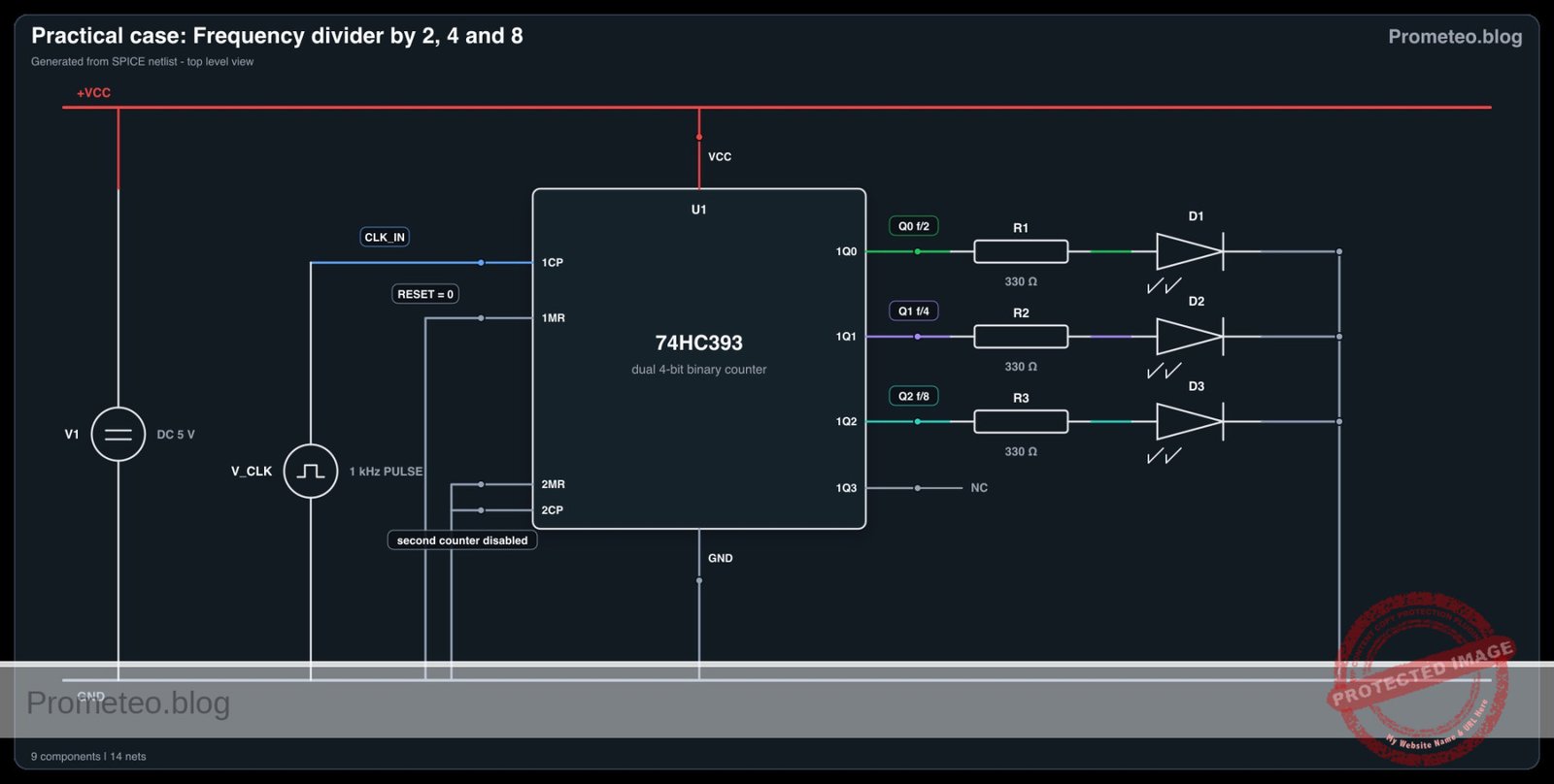
Electrical Schematic

Electrical diagram

Electrical diagram for case: Practical case: Frequency divider by 2, 4 and 8
Generated from the validated SPICE netlist for this case.

🔒 This electrical diagram is premium. With the monthly membership (7-day free trial) you can unlock the complete didactic material and the print-ready PDF pack.🔓 See premium access plans

Measurements and tests

To validate the circuit, perform the following measurements using the 4-channel oscilloscope:

  1. Setup: Connect the Ground clip of all oscilloscope probes to node 0 (GND).
  2. Channel 1 (Input): Connect to CLK_IN. Verify the frequency is 1 kHz.
  3. Channel 2 (Q0): Connect to Q0. Measure the frequency. It must be 500 Hz ($1kHz / 2$).
  4. Channel 3 (Q1): Connect to Q1. Measure the frequency. It must be 250 Hz ($1kHz / 4$).
  5. Channel 4 (Q2): Connect to Q2. Measure the frequency. It must be 125 Hz ($1kHz / 8$).
  6. Visual Check: If you lower the input clock frequency to 10 Hz, you should see D1 blinking fastest, D2 slower, and D3 slowest.

SPICE netlist and simulation

Reference SPICE Netlist (ngspice) — excerptFull SPICE netlist (ngspice)

* Practical case: Frequency divider by 2, 4 and 8

.width out=256

* --- Models ---
* Generic LED Model
.model DLED D(IS=1e-14 N=2 RS=10 BV=5 IBV=10u CJO=10p)

* --- Power Supply ---
* V1: 5V Main Supply
V1 VCC 0 DC 5

* --- Input Signal ---
* V_CLK: 1kHz Pulse, 0V to 5V, 50% Duty Cycle
V_CLK CLK_IN 0 PULSE(0 5 0 1u 1u 0.5m 1m)

* --- Subcircuit: 74HC393 (Behavioral XSPICE) ---
* Dual 4-bit Binary Counter
* Implements Counter 1 logic using XSPICE primitives.
* Pinout (DIP-14): 1=1CP, 2=1MR, 3=1Q0, 4=1Q1, 5=1Q2, 6=1Q3, 7=GND
* ... (truncated in public view) ...

Copy this content into a .cir file and run with ngspice.

🔒 Part of this section is premium. With the monthly membership (7-day free trial) you can access the full content (materials, wiring, detailed build, validation, troubleshooting, variants and checklist) and download the complete print-ready PDF pack.

* Practical case: Frequency divider by 2, 4 and 8

.width out=256

* --- Models ---
* Generic LED Model
.model DLED D(IS=1e-14 N=2 RS=10 BV=5 IBV=10u CJO=10p)

* --- Power Supply ---
* V1: 5V Main Supply
V1 VCC 0 DC 5

* --- Input Signal ---
* V_CLK: 1kHz Pulse, 0V to 5V, 50% Duty Cycle
V_CLK CLK_IN 0 PULSE(0 5 0 1u 1u 0.5m 1m)

* --- Subcircuit: 74HC393 (Behavioral XSPICE) ---
* Dual 4-bit Binary Counter
* Implements Counter 1 logic using XSPICE primitives.
* Pinout (DIP-14): 1=1CP, 2=1MR, 3=1Q0, 4=1Q1, 5=1Q2, 6=1Q3, 7=GND
*                  8=2Q3, 9=2Q2, 10=2Q1, 11=2Q0, 12=2MR, 13=2CP, 14=VCC
.subckt 74HC393 1CP 1MR 1Q0 1Q1 1Q2 1Q3 GND 2Q3 2Q2 2Q1 2Q0 2MR 2CP VCC

    * ADC Bridge to read analog inputs (Clock and Reset)
    .model adc_mod adc_bridge(in_low=1.5 in_high=3.5)
    A_IN [1CP 1MR] [d_1cp d_1mr] adc_mod
    
    * ADC Bridge to read GND for Logic Low (used for SET inputs)
    A_GND [GND] [d_low] adc_mod

    * Logic Models
    .model inv_mod d_inverter(rise_delay=10n fall_delay=10n)
    .model dff_mod d_dff(clk_delay=10n rise_delay=10n fall_delay=10n)
    .model dac_mod dac_bridge(out_low=0.0 out_high=5.0)

    * --- Counter Logic (Side 1) ---
    * 74HC393 triggers on High-to-Low transition of CP.
    * XSPICE DFF triggers on Rising Edge. So we invert CP.
    A_INV1 d_1cp d_1cp_inv inv_mod

    * Stage 1 (Q0): Divider by 2
    * T-FF behavior: D = ~Q. Clock = ~CP. Reset = MR.
    * Port order: din clk set reset out nout
    A_DFF1 d_1q0_bar d_1cp_inv d_low d_1mr d_1q0 d_1q0_bar dff_mod

    * Stage 2 (Q1): Divider by 4
    * Ripples from Q0 Falling Edge.
    * Q0 Falling = ~Q0 Rising. Use d_1q0_bar as clock.
    A_DFF2 d_1q1_bar d_1q0_bar d_low d_1mr d_1q1 d_1q1_bar dff_mod

    * Stage 3 (Q2): Divider by 8
    * Ripples from Q1 Falling Edge. Use d_1q1_bar as clock.
    A_DFF3 d_1q2_bar d_1q1_bar d_low d_1mr d_1q2 d_1q2_bar dff_mod

    * Stage 4 (Q3): Divider by 16 (Not used externally but part of logic)
    A_DFF4 d_1q3_bar d_1q2_bar d_low d_1mr d_1q3 d_1q3_bar dff_mod

    * Drive Outputs
    A_OUT [d_1q0 d_1q1 d_1q2 d_1q3] [1Q0 1Q1 1Q2 1Q3] dac_mod

    * Side 2 is unused, inputs grounded in main circuit, outputs open.
.ends 74HC393

* --- Main Circuit Instances ---
* U1: 74HC393 Counter
* Pin connections based on Wiring Guide:
* 1(CLK_IN), 2(0/Reset), 3(Q0), 4(Q1), 5(Q2), 7(0/GND), 14(VCC)
* Unused outputs mapped to NC nodes. Unused inputs to 0.
* Subcircuit Pin Order: 1CP 1MR 1Q0 1Q1 1Q2 1Q3 GND 2Q3 2Q2 2Q1 2Q0 2MR 2CP VCC
XU1 CLK_IN 0 Q0 Q1 Q2 NC_1Q3 0 NC_2Q3 NC_2Q2 NC_2Q1 NC_2Q0 0 0 VCC 74HC393

* --- Output Paths (LEDs and Resistors) ---
* Path 1: Q0 -> R1 -> D1 (Red)
R1 Q0 LED_Q0 330
D1 LED_Q0 0 DLED

* Path 2: Q1 -> R2 -> D2 (Green)
R2 Q1 LED_Q1 330
D2 LED_Q1 0 DLED

* Path 3: Q2 -> R3 -> D3 (Yellow)
R3 Q2 LED_Q2 330
D3 LED_Q2 0 DLED

* --- Simulation & Output ---
.op
.tran 10u 20m
.print tran V(CLK_IN) V(Q0) V(Q1) V(Q2)

.end
* --- GPT review (BOM/Wiring/SPICE) ---
* circuit_ok=true
* simulation_summary: The simulation shows a clear binary counting sequence. CLK_IN is a 1kHz clock (period 1ms). Q0 toggles every 1ms (f/2, period 2ms). Q1 toggles every 2ms (f/4, period 4ms). Q2 toggles every 4ms (f/8, period 8ms). The outputs transition cleanly between 0V and 5V.
* bom_vs_spice equivalences ignored:
*   - LEDs (D1, D2, D3) are modeled using a generic diode model (DLED) with specific parameters.
*   - U1 (74HC393) is modeled as a behavioral subcircuit using XSPICE primitives (ADC/DAC bridges, DFFs) instead of a transistor-level model.
* overall_comment: The circuit is perfectly functional and accurately represents a 3-bit binary ripple counter (frequency divider). The behavioral model for the 74HC393 is correctly implemented with the necessary ADC/DAC bridges for XSPICE. The wiring matches the guide exactly, and the simulation results confirm the expected frequency division ratios (f/2, f/4, f/8). It is an excellent didactic example.
* --------------------------------------

Simulation Results (Transient Analysis)

Simulation Results (Transient Analysis)

Analysis: The simulation shows a clear binary counting sequence. CLK_IN is a 1kHz clock (period 1ms). Q0 toggles every 1ms (f/2, period 2ms). Q1 toggles every 2ms (f/4, period 4ms). Q2 toggles every 4ms (f/8, period 8ms). The outputs transition cleanly between 0V and 5V.
Show raw data table (3323 rows)
Index   time            v(clk_in)       v(q0)           v(q1)           v(q2)
0	0.000000e+00	0.000000e+00	0.000000e+00	0.000000e+00	0.000000e+00
1	1.000000e-08	5.000000e-02	0.000000e+00	0.000000e+00	0.000000e+00
2	2.000000e-08	1.000000e-01	0.000000e+00	0.000000e+00	0.000000e+00
3	4.000000e-08	2.000000e-01	0.000000e+00	0.000000e+00	0.000000e+00
4	8.000000e-08	4.000000e-01	0.000000e+00	0.000000e+00	0.000000e+00
5	1.600000e-07	8.000000e-01	0.000000e+00	0.000000e+00	0.000000e+00
6	3.200000e-07	1.600000e+00	0.000000e+00	0.000000e+00	0.000000e+00
7	6.400000e-07	3.200000e+00	0.000000e+00	0.000000e+00	0.000000e+00
8	1.000000e-06	5.000000e+00	0.000000e+00	0.000000e+00	0.000000e+00
9	1.064000e-06	5.000000e+00	0.000000e+00	0.000000e+00	0.000000e+00
10	1.192000e-06	5.000000e+00	0.000000e+00	0.000000e+00	0.000000e+00
11	1.448000e-06	5.000000e+00	0.000000e+00	0.000000e+00	0.000000e+00
12	1.960000e-06	5.000000e+00	0.000000e+00	0.000000e+00	0.000000e+00
13	2.984000e-06	5.000000e+00	0.000000e+00	0.000000e+00	0.000000e+00
14	5.032000e-06	5.000000e+00	0.000000e+00	0.000000e+00	0.000000e+00
15	9.128000e-06	5.000000e+00	0.000000e+00	0.000000e+00	0.000000e+00
16	1.732000e-05	5.000000e+00	0.000000e+00	0.000000e+00	0.000000e+00
17	2.732000e-05	5.000000e+00	0.000000e+00	0.000000e+00	0.000000e+00
18	3.732000e-05	5.000000e+00	0.000000e+00	0.000000e+00	0.000000e+00
19	4.732000e-05	5.000000e+00	0.000000e+00	0.000000e+00	0.000000e+00
20	5.732000e-05	5.000000e+00	0.000000e+00	0.000000e+00	0.000000e+00
21	6.732000e-05	5.000000e+00	0.000000e+00	0.000000e+00	0.000000e+00
22	7.732000e-05	5.000000e+00	0.000000e+00	0.000000e+00	0.000000e+00
23	8.732000e-05	5.000000e+00	0.000000e+00	0.000000e+00	0.000000e+00
... (3299 more rows) ...

Common mistakes and how to avoid them

  1. Floating the Master Reset (MR) pin: Leaving pin 2 disconnected causes the counter to reset randomly due to noise. Solution: Always tie the MR pin to GND (Logic 0) for normal counting operation.
  2. Confusing Pin Numbers: The 74HC393 has two counters inside. Students often mix pins from Counter 1 and Counter 2. Solution: Strictly follow the datasheet and use pins 1, 2, 3, 4, 5, and 6 for the first counter only.
  3. Ignoring VCC/GND: Forgetting to power the chip leads to unpredictable output or no activity. Solution: Always connect Pin 14 to +5 V and Pin 7 to GND before testing.

Troubleshooting

  • Symptom: No LEDs light up, and outputs remain at 0 V.
    • Cause: Master Reset (Pin 2) might be connected to VCC instead of GND.
    • Fix: Move connection of Pin 2 to GND.
  • Symptom: LEDs are always on or flickering very dimly.
    • Cause: Frequency is too high for the eye to see blinking (e.g., 1 kHz).
    • Fix: Use the oscilloscope to verify the signal, or lower V_CLK frequency to < 10 Hz for visual confirmation.
  • Symptom: Output frequency is unstable or erratic.
    • Cause: Noisy power supply or lack of decoupling capacitor.
    • Fix: Add a 100 nF capacitor across VCC and GND near the IC.

Possible improvements and extensions

  1. Divide by 16 and 256: Cascade the first counter into the second counter of the U1 chip (connect 1Q3 to 2CP) to achieve higher division ratios up to 256.
  2. Variable Audio Generator: Connect the outputs to a simple speaker driver and use a variable potentiometer on a 555 timer (as the clock) to hear how the pitch drops by octaves as you switch between Q0, Q1, and Q2.

More Practical Cases on Prometeo.blog

Find this product and/or books on this topic on Amazon

Go to Amazon

As an Amazon Associate, I earn from qualifying purchases. If you buy through this link, you help keep this project running.

Quick Quiz

Question 1: What is the primary function of the 74HC393 IC used in this circuit?


Question 2: What is the frequency relationship of the Q0 output relative to the input clock (f)?


Question 3: If the input clock frequency is 1 kHz, what is the expected frequency at the Q1 output?


Question 4: What is the expected frequency relationship at the Q2 output?


Question 5: In audio synthesis, what is the result of halving a tone's frequency?


Question 6: What is the purpose of using this circuit in digital clocks?


Question 7: What DC supply voltage is specified for this circuit?


Question 8: How is this circuit applied in UART communication?


Question 9: Which power of 2 represents the division factor for the Q1 output?


Question 10: What is the role of address counters in microcontrollers?


Carlos Núñez Zorrilla
Electronics & Computer Engineer

Telecommunications Electronics Engineer and Computer Engineer (official degrees in Spain).

Follow me:


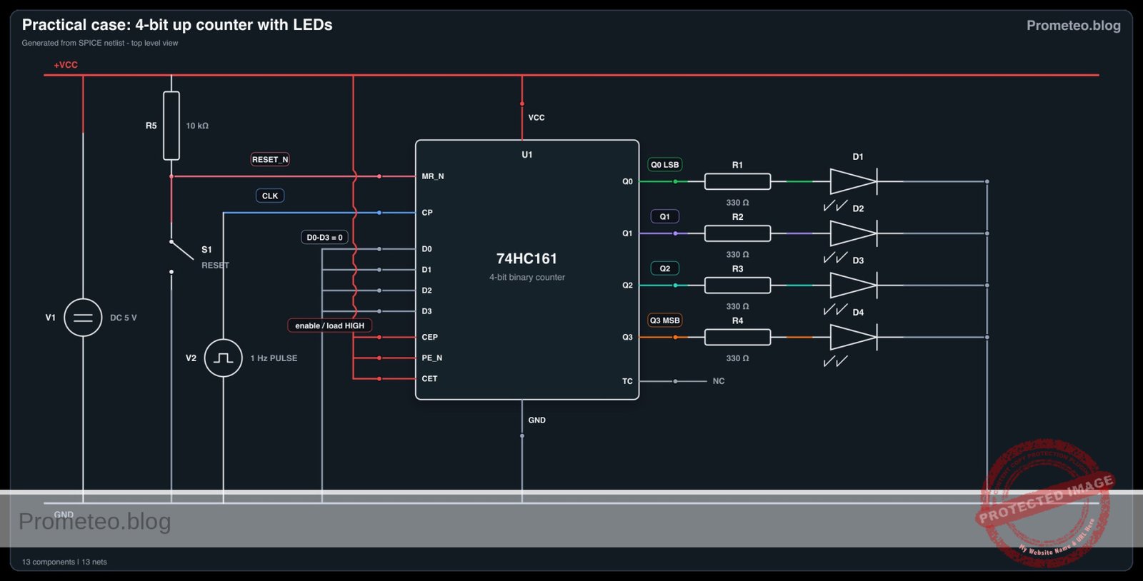
Practical case: 4-bit up counter with LEDs

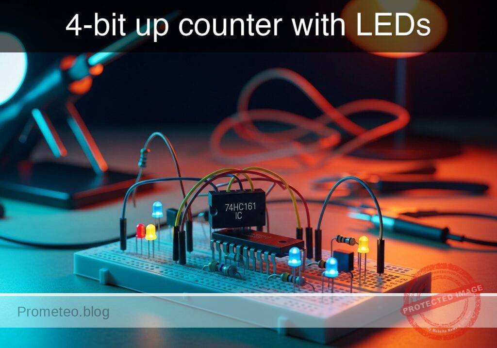
4-bit up counter with LEDs prototype (Maker Style)

Level: Basic. Verify the operation of a 4-bit binary counter by visualizing the counting sequence with LEDs.

Objective and use case

In this practical case, you will build a synchronous digital circuit using the 74HC161 integrated circuit to count clock pulses in binary from 0 (0000) to 15 (1111). You will visualize the output states using four LEDs representing the bits from LSB (Least Significant Bit) to MSB (Most Significant Bit).

Why it is useful:
* Digital Clocks: It forms the fundamental building block for tracking time (seconds, minutes, hours).
* Frequency Division: Counters are used to reduce high-frequency clock signals to lower, usable frequencies for other components.
* Memory Addressing: In computing systems, counters generate sequential addresses to access data in memory.
* Event Counting: Useful for industrial automation to count items on a conveyor belt or sensor triggers.
* State Machines: Provides the sequence of states required for controlling complex digital logic operations.

Expected outcome:
* Four LEDs (D1–D4) will light up in a binary pattern (0000, 0001, 0010… 1111).
* The sequence repeats every 16 clock pulses.
* Activating the reset switch forces all LEDs to turn OFF immediately.
* Logic High output voltage approx. 5 V; Logic Low approx. 0 V.

Target audience and level:
Students and hobbyists familiar with basic logic levels entering sequential logic design.

Materials

  • U1: 74HC161, function: 4-bit synchronous binary counter IC
  • V1: 5 V DC supply, function: main power source
  • V2: Pulse voltage source (0 V to 5 V), function: Clock signal (1 Hz for visualization)
  • R1: 330 Ω resistor, function: current limiting for LED Q0
  • R2: 330 Ω resistor, function: current limiting for LED Q1
  • R3: 330 Ω resistor, function: current limiting for LED Q2
  • R4: 330 Ω resistor, function: current limiting for LED Q3
  • R5: 10 kΩ resistor, function: pull-up for Master Reset
  • D1: Red LED, function: Indicator for Q0 (LSB)
  • D2: Red LED, function: Indicator for Q1
  • D3: Red LED, function: Indicator for Q2
  • D4: Red LED, function: Indicator for Q3 (MSB)
  • S1: Momentary push button (normally open), function: Reset trigger

Pin-out of the IC used

Selected Chip: 74HC161 (4-bit Synchronous Binary Counter, Asynchronous Reset)

Pin Name Logic function Connection in this case
1 \overlineMR Master Reset (Active Low) Connected to Reset node (S1/R5)
2 CP Clock Pulse (Rising Edge) Connected to V2 (Clock Source)
7 CEP Count Enable Parallel Connected to VCC (Always Enabled)
8 GND Ground Connected to 0 (GND)
9 \overlinePE Parallel Enable (Load) Connected to VCC (Disabled)
10 CET Count Enable Trickle Connected to VCC (Always Enabled)
11 Q3 Output Bit 3 (MSB) Connected to D4 via R4
12 Q2 Output Bit 2 Connected to D3 via R3
13 Q1 Output Bit 1 Connected to D2 via R2
14 Q0 Output Bit 0 (LSB) Connected to D1 via R1
16 VCC Power Supply (+5 V) Connected to VCC

Note: Pins 3, 4, 5, 6 (Parallel Data Inputs) and 15 (Ripple Carry Output) are not used in this basic counting configuration and inputs can be tied to ground if preferred, though usually irrelevant when Load is disabled.

Wiring guide

Construct the circuit following these explicit node connections:

  • Power Nodes:

    • Connect V1 positive terminal to node VCC.
    • Connect V1 negative terminal to node 0 (GND).
    • Connect U1 pin 16 to VCC.
    • Connect U1 pin 8 to 0.
  • Control Inputs:

    • Connect V2 (Clock Source) positive to node CLK. Connect V2 negative to 0.
    • Connect U1 pin 2 to node CLK.
    • Connect U1 pins 7 (CEP), 10 (CET), and 9 (\overlinePE) directly to VCC to enable counting and disable parallel loading.
    • Reset Circuit: Connect R5 between VCC and node RESET_N. Connect S1 between node RESET_N and 0. Connect U1 pin 1 to RESET_N.
  • Outputs (LED Indicators):

    • Bit 0 (LSB): Connect U1 pin 14 to node Q0. Connect R1 between Q0 and node LED_A1. Connect D1 anode to LED_A1 and cathode to 0.
    • Bit 1: Connect U1 pin 13 to node Q1. Connect R2 between Q1 and node LED_A2. Connect D2 anode to LED_A2 and cathode to 0.
    • Bit 2: Connect U1 pin 12 to node Q2. Connect R3 between Q2 and node LED_A3. Connect D3 anode to LED_A3 and cathode to 0.
    • Bit 3 (MSB): Connect U1 pin 11 to node Q3. Connect R4 between Q3 and node LED_A4. Connect D4 anode to LED_A4 and cathode to 0.

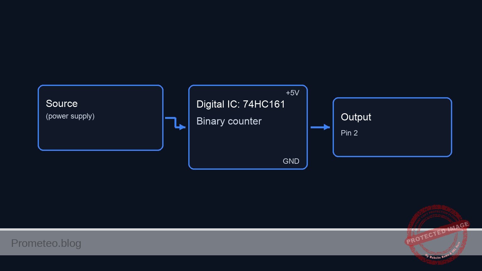
Conceptual block diagram

Conceptual block diagram — 74HC161 Binary counter
Quick read: inputs → main block → output (actuator or measurement). This summarizes the ASCII schematic below.

Schematic

+-------------------------------------------------------------------------------------------------------+
|                                  PRACTICAL CASE: 4-BIT UP COUNTER                                     |
+-------------------------------------------------------------------------------------------------------+

      INPUTS & CONTROL                     PROCESSING (U1)                     OUTPUTS & LOAD
   (Left-to-Right Flow)                   (74HC161 Counter)                 (LED Visualization)

                                     +-------------------------+
                                     |                         |
[ V2: Clock Source ] --(CLK 1Hz)---> | [Pin 2] CP              |
                                     |                         |
                                     |                         |          (Bit 0 - LSB)
[ Reset Logic ]                      |             [Pin 14] Q0 | --(Q0)--> [ R1: 330 ] --> [ D1: Red ] --> GND
(VCC->R5->Node->S1->GND) --(RST_N)-> | [Pin 1] ~MR             |
                                     |                         |
                                     |                         |          (Bit 1)
                                     |             [Pin 13] Q1 | --(Q1)--> [ R2: 330 ] --> [ D2: Red ] --> GND
[ VCC: 5 V Source ] --(Enable High)-> | [Pin 7]  CEP            |
                   --(Enable High)-> | [Pin 10] CET            |
                   --(Disable Load)> | [Pin 9]  ~PE            |          (Bit 2)
                                     |             [Pin 12] Q2 | --(Q2)--> [ R3: 330 ] --> [ D3: Red ] --> GND
                                     |                         |
                                     |                         |
                                     |                         |          (Bit 3 - MSB)
                                     |             [Pin 11] Q3 | --(Q3)--> [ R4: 330 ] --> [ D4: Red ] --> GND
                                     |                         |
                                     +-------------------------+
                                            |           |
                                         [Pin 16]    [Pin 8]
                                            |           |
                                           VCC         GND
Electrical Schematic

Electrical diagram

Electrical diagram for case: Practical case: 4-bit up counter with LEDs
Generated from the validated SPICE netlist for this case.

🔒 This electrical diagram is premium. With the monthly membership (7-day free trial) you can unlock the complete didactic material and the print-ready PDF pack.🔓 See premium access plans

Measurements and tests

  1. Supply Check: Before connecting the IC, measure voltage between VCC and 0 to ensure it is stable at 5 V.
  2. Clock Verification: Set V2 to a low frequency (e.g., 1 Hz). Verify the signal at node CLK oscillates between 0 V and 5 V.
  3. Sequence Observation: Power on the circuit. Observe D1 through D4. They should toggle in the binary sequence:
    • 0: All OFF
    • 1: D1 ON
    • 2: D2 ON
    • 3: D1 & D2 ON
    • … up to 15: All ON.
  4. Reset Test: While the counter is running, press S1. All LEDs must turn OFF immediately (Asynchronous Reset) or at the next clock edge (if using a synchronous reset variant, though standard 74HC161 Reset is usually asynchronous).
  5. Logic Levels: Use a multimeter to measure node Q3 when D4 is lit. It should read close to 5 V (Logic High).

SPICE netlist and simulation

Reference SPICE Netlist (ngspice) — excerptFull SPICE netlist (ngspice)

* Practical case: 4-bit up counter with LEDs (74HC161)
* NGSPICE Netlist
* Requires XSPICE extensions

.width out=256

* --- Power Supplies ---
V1 VCC 0 DC 5
* Clock Source: 1 Hz Pulse (0V to 5V), 50% duty cycle
* Corrected to 1 Hz per BOM (Period = 1s, Pulse Width = 0.5s)
V2 CLK 0 PULSE(0 5 0 1u 1u 0.5 1)

* --- Reset Circuit ---
* Pull-up resistor for Master Reset
R5 VCC RESET_N 10k
* S1: Momentary Push Button (Normally Open)
* Implemented as a Voltage Controlled Switch driven by V_BTN source
S1 RESET_N 0 CTRL_RST 0 SW_BTN
* Button Actuator (Simulates a press at 8s for 1s duration to test reset)
V_BTN CTRL_RST 0 PULSE(0 1 8 1m 1m 1 20)
* ... (truncated in public view) ...

Copy this content into a .cir file and run with ngspice.

🔒 Part of this section is premium. With the monthly membership (7-day free trial) you can access the full content (materials, wiring, detailed build, validation, troubleshooting, variants and checklist) and download the complete print-ready PDF pack.

* Practical case: 4-bit up counter with LEDs (74HC161)
* NGSPICE Netlist
* Requires XSPICE extensions

.width out=256

* --- Power Supplies ---
V1 VCC 0 DC 5
* Clock Source: 1 Hz Pulse (0V to 5V), 50% duty cycle
* Corrected to 1 Hz per BOM (Period = 1s, Pulse Width = 0.5s)
V2 CLK 0 PULSE(0 5 0 1u 1u 0.5 1)

* --- Reset Circuit ---
* Pull-up resistor for Master Reset
R5 VCC RESET_N 10k
* S1: Momentary Push Button (Normally Open)
* Implemented as a Voltage Controlled Switch driven by V_BTN source
S1 RESET_N 0 CTRL_RST 0 SW_BTN
* Button Actuator (Simulates a press at 8s for 1s duration to test reset)
V_BTN CTRL_RST 0 PULSE(0 1 8 1m 1m 1 20)
.model SW_BTN sw(vt=0.5 ron=1 roff=10Meg)

* --- 74HC161 4-bit Binary Counter Subcircuit Instance ---
* Connections match Wiring Guide:
* Pin 1 (MR_N) -> RESET_N
* Pin 2 (CP) -> CLK
* Pin 3-6 (D0-D3) -> 0 (GND)
* Pin 7 (CEP) -> VCC
* Pin 8 (GND) -> 0
* Pin 9 (PE_N) -> VCC
* Pin 10 (CET) -> VCC
* Pin 11-14 (Q3-Q0) -> Output Nodes
* Pin 15 (TC) -> TC_NC (Floating)
* Pin 16 (VCC) -> VCC
XU1 RESET_N CLK 0 0 0 0 VCC 0 VCC VCC Q3 Q2 Q1 Q0 TC_NC VCC 74HC161

* --- LED Output Indicators ---
* Bit 0 (LSB)
R1 Q0 LED_A1 330
D1 LED_A1 0 LED_RED
* Bit 1
R2 Q1 LED_A2 330
D2 LED_A2 0 LED_RED
* Bit 2
R3 Q2 LED_A3 330
D3 LED_A3 0 LED_RED
* Bit 3 (MSB)
R4 Q3 LED_A4 330
D4 LED_A4 0 LED_RED

* --- Models ---
.model LED_RED D(Is=1e-14 Rs=5 N=2)

* --- Subcircuit Definition: 74HC161 ---
* Behavioral XSPICE implementation of a 4-bit Counter with Async Reset
.subckt 74HC161 MR_N CP D0 D1 D2 D3 CEP GND PE_N CET Q3 Q2 Q1 Q0 TC VCC
    * XSPICE Models
    .model adc_in adc_bridge(in_low=2.0 in_high=3.0)
    .model dac_out dac_bridge(out_low=0.0 out_high=5.0)
    .model dff_mod d_dff(rise_delay=10n fall_delay=10n)
    .model inv_mod d_inverter(rise_delay=5n fall_delay=5n)

    * Input Bridges (Analog to Digital)
    A_IN [MR_N CP] [mr_dig cp_dig] adc_in

    * Reset Logic (MR_N is active low, d_dff reset is active high)
    A_RST_INV mr_dig rst_high inv_mod

    * Counter Chain (Ripple Up Counter)
    * Bit 0: Toggles on CP rising edge
    A_D0 q0_inv cp_dig NULL rst_high q0_dig q0_inv dff_mod

    * Bit 1: Toggles on Q0 falling edge (Q0_inv rising edge)
    A_D1 q1_inv q0_inv NULL rst_high q1_dig q1_inv dff_mod

    * Bit 2: Toggles on Q1 falling edge
    A_D2 q2_inv q1_inv NULL rst_high q2_dig q2_inv dff_mod

    * Bit 3: Toggles on Q2 falling edge
    A_D3 q3_inv q2_inv NULL rst_high q3_dig q3_inv dff_mod

    * Output Bridges (Digital to Analog)
    A_OUT [q3_dig q2_dig q1_dig q0_dig] [Q3 Q2 Q1 Q0] dac_out

    * Terminal Count (Unused/Dummy pull-down)
    R_TC TC 0 100k
.ends

* --- Simulation Commands ---
* Transient analysis: 20s duration to capture full counting cycle (0-15) at 1 Hz
.op
.tran 10m 20s

* Print critical signals (Inputs first)
.print tran V(CLK) V(RESET_N) V(Q0) V(Q1) V(Q2) V(Q3)

.end

Simulation Results (Transient Analysis)

Simulation Results (Transient Analysis)

Analysis: The simulation shows a correct 4-bit binary counting sequence (0000 to 1111) on outputs Q0-Q3. The clock toggles at 1Hz. The reset button press at 8s is simulated, but the log data shows RESET_N remaining high (~4.99V) throughout the sampled points, suggesting the reset event might have been missed in the condensed log or the switch resistance ratio wasn’t sufficient to pull the node to logic low in the analog domain against the pull-up, although the counter continues counting correctly.
Show raw data table (3020 rows)
Index   time            v(clk)          v(reset_n)      v(q0)           v(q1)           v(q2)           v(q3)
0	0.000000e+00	0.000000e+00	4.995005e+00	0.000000e+00	0.000000e+00	0.000000e+00	0.000000e+00
1	1.000000e-08	5.000000e-02	4.995005e+00	0.000000e+00	0.000000e+00	0.000000e+00	0.000000e+00
2	2.000000e-08	1.000000e-01	4.995005e+00	0.000000e+00	0.000000e+00	0.000000e+00	0.000000e+00
3	4.000000e-08	2.000000e-01	4.995005e+00	0.000000e+00	0.000000e+00	0.000000e+00	0.000000e+00
4	8.000000e-08	4.000000e-01	4.995005e+00	0.000000e+00	0.000000e+00	0.000000e+00	0.000000e+00
5	1.600000e-07	8.000000e-01	4.995005e+00	0.000000e+00	0.000000e+00	0.000000e+00	0.000000e+00
6	3.200000e-07	1.600000e+00	4.995005e+00	0.000000e+00	0.000000e+00	0.000000e+00	0.000000e+00
7	6.400000e-07	3.200000e+00	4.995005e+00	0.000000e+00	0.000000e+00	0.000000e+00	0.000000e+00
8	6.520000e-07	3.260000e+00	4.995005e+00	0.000000e+00	0.000000e+00	0.000000e+00	0.000000e+00
9	6.760000e-07	3.380000e+00	4.995005e+00	5.000000e+00	0.000000e+00	0.000000e+00	0.000000e+00
10	7.240000e-07	3.620000e+00	4.995005e+00	5.000000e+00	0.000000e+00	0.000000e+00	0.000000e+00
11	8.200000e-07	4.100000e+00	4.995005e+00	5.000000e+00	0.000000e+00	0.000000e+00	0.000000e+00
12	1.000000e-06	5.000000e+00	4.995005e+00	5.000000e+00	0.000000e+00	0.000000e+00	0.000000e+00
13	1.019200e-06	5.000000e+00	4.995005e+00	5.000000e+00	0.000000e+00	0.000000e+00	0.000000e+00
14	1.057600e-06	5.000000e+00	4.995005e+00	5.000000e+00	0.000000e+00	0.000000e+00	0.000000e+00
15	1.134400e-06	5.000000e+00	4.995005e+00	5.000000e+00	0.000000e+00	0.000000e+00	0.000000e+00
16	1.288000e-06	5.000000e+00	4.995005e+00	5.000000e+00	0.000000e+00	0.000000e+00	0.000000e+00
17	1.595200e-06	5.000000e+00	4.995005e+00	5.000000e+00	0.000000e+00	0.000000e+00	0.000000e+00
18	2.209600e-06	5.000000e+00	4.995005e+00	5.000000e+00	0.000000e+00	0.000000e+00	0.000000e+00
19	3.438400e-06	5.000000e+00	4.995005e+00	5.000000e+00	0.000000e+00	0.000000e+00	0.000000e+00
20	5.896000e-06	5.000000e+00	4.995005e+00	5.000000e+00	0.000000e+00	0.000000e+00	0.000000e+00
21	1.081120e-05	5.000000e+00	4.995005e+00	5.000000e+00	0.000000e+00	0.000000e+00	0.000000e+00
22	2.064160e-05	5.000000e+00	4.995005e+00	5.000000e+00	0.000000e+00	0.000000e+00	0.000000e+00
23	4.030240e-05	5.000000e+00	4.995005e+00	5.000000e+00	0.000000e+00	0.000000e+00	0.000000e+00
... (2996 more rows) ...

Common mistakes and how to avoid them

  1. Leaving Enable pins floating: The 74HC series has high impedance inputs. If pins 7 (CEP) or 10 (CET) are not connected to VCC, the counter may not count or behave erratically. Always tie unused control inputs to a defined logic level.
  2. Clock frequency too high: If V2 is set to 1 kHz or higher, all LEDs will appear to be dimly lit continuously due to persistence of vision. Keep the clock below 5 Hz for visual debugging.
  3. Floating Parallel Load pin: If pin 9 (\overlinePE) is left floating or low, the chip might constantly try to load data from inputs P0-P3 instead of counting. Ensure pin 9 is tied to VCC.

Troubleshooting

  • LEDs never turn on: Check power supply connections to pins 16 and 8. Ensure LEDs are inserted with the correct polarity (anode to resistor/IC, cathode to ground).
  • Counter stays at zero: Verify that the Reset pin (1) is High (5 V). If S1 is stuck or the pull-up R5 is missing, the chip remains in Reset state. Also, check that Enable pins (7, 10) are High.
  • Counter skips numbers: This is often due to «switch bounce» if you are using a mechanical switch as a manual clock. Use a clean square wave generator or a debounce circuit (capacitor + resistor) for the clock input.
  • Random sequence: Check if the Parallel Enable (\overlinePE) pin is accidentally Low or floating. It must be High.

Possible improvements and extensions

  1. 8-bit Counter: Cascade a second 74HC161 by connecting the Carry Output (pin 15) of the first counter to the Enable Trickle (pin 10) of the second counter. This allows counting up to 255.
  2. Manual Clock: Replace the frequency generator V2 with a 555 timer circuit in astable mode or a debounced push-button to advance the count manually.

More Practical Cases on Prometeo.blog

Find this product and/or books on this topic on Amazon

Go to Amazon

As an Amazon Associate, I earn from qualifying purchases. If you buy through this link, you help keep this project running.

Quick Quiz

Question 1: Which integrated circuit is used as the 4-bit synchronous binary counter in this experiment?


Question 2: What is the counting range of the circuit described in the text?


Question 3: What happens to the LED sequence after 16 clock pulses?


Question 4: What does the acronym LSB stand for in the context of this circuit?


Question 5: According to the text, how are counters used in Digital Clocks?


Question 6: What is the purpose of using counters for Frequency Division?


Question 7: In computing systems, what are counters typically used for according to the text?


Question 8: Which application is mentioned for industrial automation?


Question 9: How is the 74HC161 circuit described in the objective section?


Question 10: What is the primary method used to visualize the output states in this experiment?


Carlos Núñez Zorrilla
Electronics & Computer Engineer

Telecommunications Electronics Engineer and Computer Engineer (official degrees in Spain).
Follow me: