Practical case: NE555 Delay-On Timer for READY Indicator

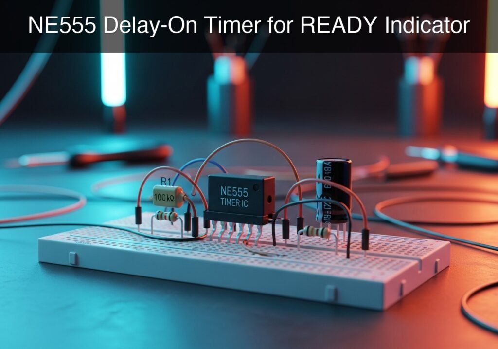
NE555 Delay-On Timer for READY Indicator prototype (Maker Style)

Level: Basic – Build an RC-timed delay circuit to activate a READY indicator seconds after power is applied.

Objective and use case

In this practical case, you will build a delay-on timer using the versatile NE555 integrated circuit. Upon applying 5 V power, an RC network dictates a waiting period before the timer’s output activates and turns on a «READY» LED.

This timer topology is highly useful in real-world applications:
* Audio amplifiers: Delaying speaker connection until internal voltages stabilize to prevent loud popping noises.
* Power supply sequencing: Ensuring primary rails are fully powered before activating secondary logic circuits.
* Microcontroller resets: Holding a reset line active for a brief period during startup to guarantee clean initialization.

Expected outcome:
* At power-on ($t=0$), the LED will remain OFF.
* The voltage at the timing node (VCAP) will exponentially decay from 5 V down to 1.66 V (which is 1/3 VCC).
* Once VCAP crosses the 1.66 V threshold, the NE555 output (VOUT) will snap from 0 V to 5 V (HIGH), illuminating the LED.
* The delay time will be approximately 5.1 seconds.

Target audience and level: Beginners learning analog-digital timing and RC time constants.

Materials

  • U1: NE555 timer IC, function: timing controller
  • R1: 100 kΩ resistor, function: timing resistor
  • C1: 47 µF electrolytic capacitor, function: timing capacitor
  • R2: 330 Ω resistor, function: LED current limiting
  • C2: 10 nF ceramic capacitor, function: control voltage stabilization
  • D1: green LED, function: READY indicator
  • V1: 5 V DC supply

Pin-out of the IC used

NE555 Timer IC

Pin Name Logic/Analog function Connection in this case
1 GND Ground reference Node 0
2 TRIG Trigger input (active low, < 1/3 VCC) Node VCAP
3 OUT Output Node VOUT
4 RESET Reset input (active low) Node VCC
5 CTRL Control voltage access Node VCTRL
6 THR Threshold input (active high, > 2/3 VCC) Node VCAP
7 DISCH Discharge open-collector Not connected
8 VCC Supply voltage Node VCC

Wiring guide

  • V1: connects between VCC (+5 V) and 0 (GND).
  • C1: connects between VCC (positive leg) and VCAP (negative leg).
  • R1: connects between VCAP and 0.
  • U1 connections:
  • Pin 1 (GND) connects to 0.
  • Pin 2 (TRIG) connects to VCAP.
  • Pin 3 (OUT) connects to VOUT.
  • Pin 4 (RESET) connects to VCC.
  • Pin 5 (CTRL) connects to VCTRL.
  • Pin 6 (THR) connects to VCAP.
  • Pin 8 (VCC) connects to VCC.
  • C2: connects between VCTRL and 0.
  • R2: connects between VOUT and VLED.
  • D1: connects between VLED (anode) and 0 (cathode).

Conceptual block diagram
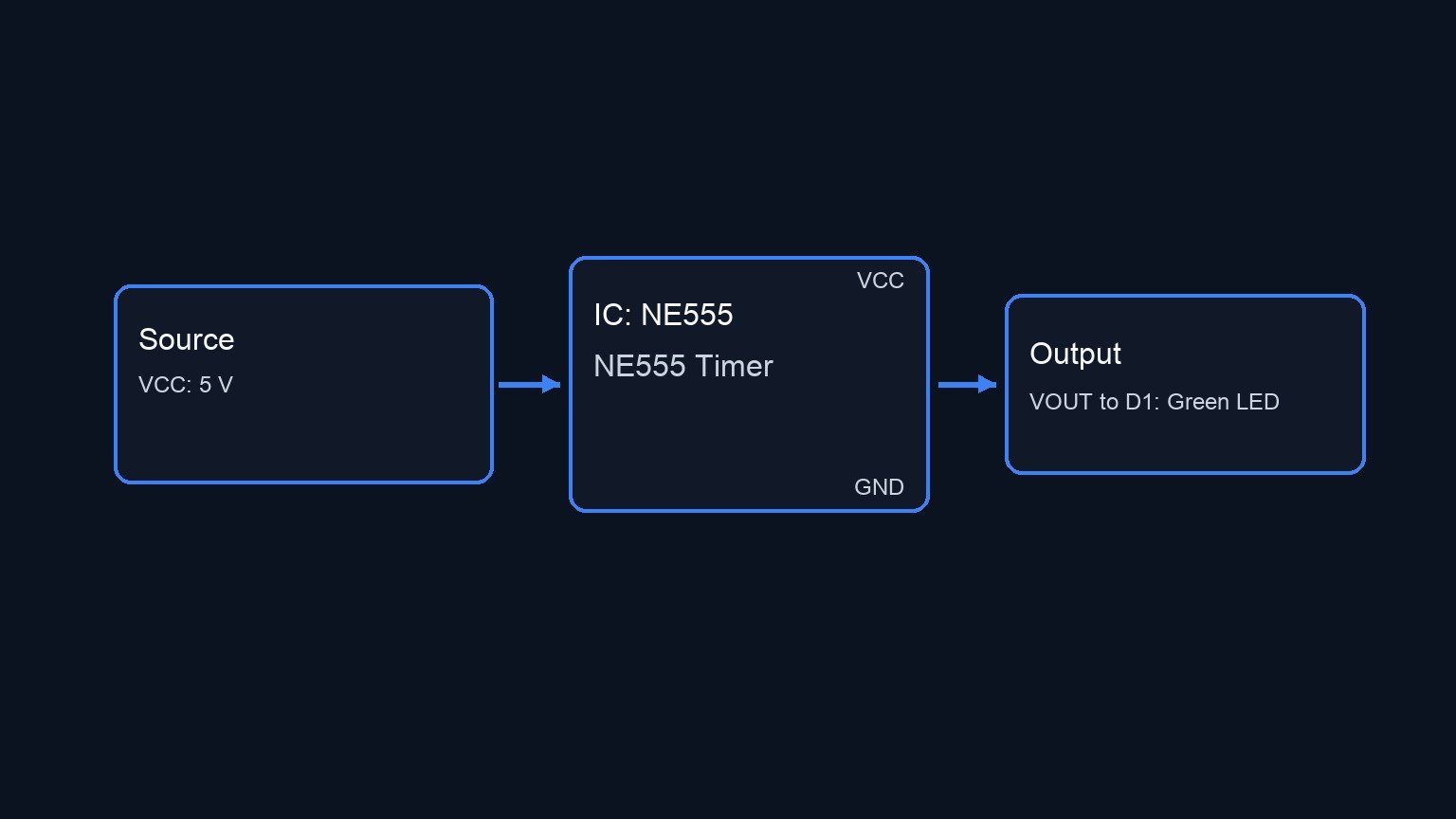
Conceptual block diagram — NE555 NE555 Timer
Quick read: inputs → main block → output (actuator or measurement). This summarizes the ASCII schematic below.

Schematic

[ VCC: 5 V ] --> [ C1: 47µF ] --(VCAP)--> [ U1: NE555 Timer ] --(VOUT)--> [ R2: 330 Ω ] --(VLED)--> [ D1: Green LED ] --> GND
                                         [ Pin 2: TRIG     ]
[ VCAP Node ] -> [ R1: 100 kΩ ] -> GND    [ Pin 6: THR      ]
                                         [ Pin 4: RESET    ] <--- [ VCC: 5 V ]
                                         [ Pin 8: VCC      ] <--- [ VCC: 5 V ]
                                         [ Pin 5: CTRL     ] --(VCTRL)--> [ C2: 10nF ] --> GND
                                         [ Pin 1: GND      ] ---> GND
Electrical Schematic

Measurements and tests

To validate the transient behavior of this delay-on timer, perform the following steps:

  1. Initial State Verification: Ensure power is completely disconnected. Use a multimeter or oscilloscope to confirm that VCAP and VOUT are at 0 V.
  2. Apply Power: Turn on the 5 V supply (V1). Start a stopwatch immediately. Verify that VOUT is initially ~0 V and the LED is OFF.
  3. Transient Validation of VCAP: Measure the voltage at node VCAP with respect to ground (0). Because the capacitor C1 is tied to VCC, it acts as a short circuit at $t=0$, pulling VCAP to 5 V. As C1 charges through R1, observe VCAP exponentially decaying toward 0 V.
  4. Trigger Threshold: Monitor VCAP as it drops. Exactly as it crosses 1.66 V (1/3 of VCC), verify that VOUT instantly jumps to 5 V and the READY LED illuminates.
  5. Timing Calculation: Verify the elapsed time. The theoretical delay for this configuration is calculated as T ≈ 1.1 × R × C. With 100 kΩ and 47 µF, T ≈ 5.17 seconds. Check that your measured time aligns with this estimate.

SPICE netlist and simulation

Reference SPICE Netlist (ngspice) — excerptFull SPICE netlist (ngspice)

* Practical case: NE555 Delay-On Timer for READY Indicator
.width out=256

* Power Supply (Pulse to simulate power-on and provide dynamic stimulus)
V1 VCC 0 PULSE(0 5 0 100u 100u 10 10)

* Timing Capacitor and Resistor
C1 VCC VCAP 47uF
R1 VCAP 0 100k

* Control Voltage Stabilization Capacitor
C2 VCTRL 0 10nF

* Output Current Limiting Resistor and LED
R2 VOUT VLED 330
D1 VLED 0 DLED

* NE555 Timer IC Instantiation
* Wiring: Pin 1 (GND)=0, Pin 2 (TRIG)=VCAP, Pin 3 (OUT)=VOUT, Pin 4 (RESET)=VCC, Pin 5 (CTRL)=VCTRL, Pin 6 (THR)=VCAP, Pin 8 (VCC)=VCC
XU1 0 VCAP VOUT VCC VCTRL VCAP VCC NE555
* ... (truncated in public view) ...

Copy this content into a .cir file and run with ngspice.

* Practical case: NE555 Delay-On Timer for READY Indicator
.width out=256

* Power Supply (Pulse to simulate power-on and provide dynamic stimulus)
V1 VCC 0 PULSE(0 5 0 100u 100u 10 10)

* Timing Capacitor and Resistor
C1 VCC VCAP 47uF
R1 VCAP 0 100k

* Control Voltage Stabilization Capacitor
C2 VCTRL 0 10nF

* Output Current Limiting Resistor and LED
R2 VOUT VLED 330
D1 VLED 0 DLED

* NE555 Timer IC Instantiation
* Wiring: Pin 1 (GND)=0, Pin 2 (TRIG)=VCAP, Pin 3 (OUT)=VOUT, Pin 4 (RESET)=VCC, Pin 5 (CTRL)=VCTRL, Pin 6 (THR)=VCAP, Pin 8 (VCC)=VCC
XU1 0 VCAP VOUT VCC VCTRL VCAP VCC NE555

* LED Model
.model DLED D(IS=1e-15 N=2.0 RS=10)

* NE555 Subcircuit (Robust Continuous Behavioral Model)
.subckt NE555 GND TRIG OUT RESET CTRL THR VCC
* Internal voltage divider
R1 VCC CTRL 5k
R2 CTRL N1 5k
R3 N1 GND 5k

* Smooth Comparators using tanh to prevent convergence issues
B_TH COMP_TH GND V=0.5*(1+tanh((V(THR)-V(CTRL))*100))
B_TR COMP_TR GND V=0.5*(1+tanh((V(N1)-V(TRIG))*100))
B_RST RST_INT GND V=0.5*(1+tanh((0.7-V(RESET))*100))

* Continuous SR Latch State Equation
B_Q Q_IN GND V=V(COMP_TR) + V(Q_OUT)*(1-V(COMP_TH)) - V(RST_INT)
R4 Q_IN Q_NODE 1k
C3 Q_NODE GND 1nF
B_Q_OUT Q_OUT GND V=0.5*(1+tanh((V(Q_NODE)-0.5)*10))

* Output stage with small series resistance
B_OUT OUT_INT GND V=V(VCC)*V(Q_OUT)
R_OUT OUT_INT OUT 10
.ends

* Transient Analysis
.op
.tran 10m 10
.print tran V(VCC) V(VOUT) V(VCAP) V(VLED) V(VCTRL)

Simulation Results (Transient Analysis)

Simulation Results (Transient Analysis)
Analysis: The transient analysis spans 0 s to 10 s and captures the switching interval. Main ranges: v(vout) -4.47e-08 uV -> 4.9 V; v(vctrl) 0 uV -> 3.33 V; v(vcap) 0 uV -> 5 V.
Show raw data table (1048 rows)
Index   time            v(vcc)          v(vout)         v(vcap)         v(vled)         v(vctrl)
0	0.000000e+00	0.000000e+00	4.832629e-31	0.000000e+00	1.643094e-29	0.000000e+00
1	1.000000e-06	5.000000e-02	2.776793e-25	4.999999e-02	2.777048e-25	9.708738e-04
2	1.084000e-06	5.420000e-02	5.111901e-13	5.419999e-02	5.111901e-13	1.059260e-03
3	1.252000e-06	6.260000e-02	2.888571e-13	6.259999e-02	2.888571e-13	1.249666e-03
4	1.588000e-06	7.940000e-02	1.193784e-13	7.939999e-02	1.193784e-13	1.711860e-03
5	2.260000e-06	1.130000e-01	3.159549e-15	1.130000e-01	3.159549e-15	2.957719e-03
6	3.604000e-06	1.802000e-01	-4.46777e-14	1.801999e-01	-4.46777e-14	6.703556e-03
7	5.753920e-06	2.876960e-01	1.153350e-14	2.876958e-01	1.153350e-14	1.602982e-02
8	8.529919e-06	4.264960e-01	3.920905e-14	4.264956e-01	3.920905e-14	3.378163e-02
9	1.323373e-05	6.616863e-01	6.229971e-14	6.616853e-01	6.229971e-14	7.714122e-02
10	1.776006e-05	8.880031e-01	7.679640e-08	8.880014e-01	7.679640e-08	1.330167e-01
11	2.207156e-05	1.103578e+00	4.718975e-04	1.103575e+00	4.718975e-04	1.975078e-01
12	2.551739e-05	1.275870e+00	3.176107e-05	1.275866e+00	3.176107e-05	2.560560e-01
13	2.635388e-05	1.317694e+00	4.676638e-05	1.317690e+00	4.676638e-05	2.711361e-01
14	2.687674e-05	1.343837e+00	5.278079e-05	1.343833e+00	5.278079e-05	2.807240e-01
15	2.751921e-05	1.375961e+00	5.781702e-05	1.375957e+00	5.781702e-05	2.926720e-01
16	2.815313e-05	1.407657e+00	6.142719e-05	1.407652e+00	6.142719e-05	3.046382e-01
17	2.880258e-05	1.440129e+00	6.412060e-05	1.440125e+00	6.412060e-05	3.170766e-01
18	2.949081e-05	1.474541e+00	6.629097e-05	1.474536e+00	6.629097e-05	3.304515e-01
19	3.016263e-05	1.508132e+00	6.813606e-05	1.508127e+00	6.813606e-05	3.436961e-01
20	3.083350e-05	1.541675e+00	6.982103e-05	1.541670e+00	6.982103e-05	3.571040e-01
21	3.149330e-05	1.574665e+00	7.140022e-05	1.574660e+00	7.140022e-05	3.704649e-01
22	3.216372e-05	1.608186e+00	7.296437e-05	1.608181e+00	7.296437e-05	3.842142e-01
23	3.283050e-05	1.641525e+00	7.449937e-05	1.641519e+00	7.449937e-05	3.980585e-01
... (1024 more rows) ...


Reference SPICE netlist (ngspice)

* Practical case: NE555 Delay-On Timer for READY Indicator
.width out=256

* Power Supply (Pulse to simulate power-on and provide dynamic stimulus)
V1 VCC 0 PULSE(0 5 0 100u 100u 10 10)

* Timing Capacitor and Resistor
C1 VCC VCAP 47uF
R1 VCAP 0 100k

* Control Voltage Stabilization Capacitor
C2 VCTRL 0 10nF

* Output Current Limiting Resistor and LED
R2 VOUT VLED 330
D1 VLED 0 DLED

* NE555 Timer IC Instantiation
* Wiring: Pin 1 (GND)=0, Pin 2 (TRIG)=VCAP, Pin 3 (OUT)=VOUT, Pin 4 (RESET)=VCC, Pin 5 (CTRL)=VCTRL, Pin 6 (THR)=VCAP, Pin 8 (VCC)=VCC
XU1 0 VCAP VOUT VCC VCTRL VCAP VCC NE555

* LED Model
.model DLED D(IS=1e-15 N=2.0 RS=10)

* NE555 Subcircuit (Robust Continuous Behavioral Model)
.subckt NE555 GND TRIG OUT RESET CTRL THR VCC
* Internal voltage divider
R1 VCC CTRL 5k
R2 CTRL N1 5k
R3 N1 GND 5k

* Smooth Comparators using tanh to prevent convergence issues
B_TH COMP_TH GND V=0.5*(1+tanh((V(THR)-V(CTRL))*100))
B_TR COMP_TR GND V=0.5*(1+tanh((V(N1)-V(TRIG))*100))
B_RST RST_INT GND V=0.5*(1+tanh((0.7-V(RESET))*100))

* Continuous SR Latch State Equation
B_Q Q_IN GND V=V(COMP_TR) + V(Q_OUT)*(1-V(COMP_TH)) - V(RST_INT)
R4 Q_IN Q_NODE 1k
C3 Q_NODE GND 1nF
B_Q_OUT Q_OUT GND V=0.5*(1+tanh((V(Q_NODE)-0.5)*10))

* Output stage with small series resistance
B_OUT OUT_INT GND V=V(VCC)*V(Q_OUT)
R_OUT OUT_INT OUT 10
.ends

* Transient Analysis
.op
.tran 10m 10
.print tran V(VCC) V(VOUT) V(VCAP) V(VLED) V(VCTRL)

Simulation Results (Transient Analysis)

Simulation Results (Transient Analysis)
Analysis: The transient analysis spans 0 s to 10 s and captures the switching interval. Main ranges: v(vout) -4.47e-08 uV -> 4.9 V; v(vctrl) 0 uV -> 3.33 V; v(vcap) 0 uV -> 5 V.

Common mistakes and how to avoid them

  • Reversing the R and C positions: Connecting R1 to VCC and C1 to 0 creates a delay-off timer rather than a delay-on timer. Ensure C1 connects strictly to VCC and R1 to 0 to achieve the desired power-on delay.
  • Leaving the RESET pin floating: An unconnected Pin 4 can pick up ambient electrical noise, causing the timer to reset randomly and preventing the LED from turning on. Always tie Pin 4 directly to VCC.
  • Electrolytic capacitor reverse polarity: In this specific configuration, the positive terminal of C1 must go to VCC and the negative terminal to VCAP. Reversing this will cause high leakage current, drastically altering the delay time or destroying the capacitor.


Troubleshooting

  • Symptom: LED turns on instantly without delay.
    • Cause: C1 is internally shorted, or the R1/C1 components were swapped.
    • Fix: Double-check the wiring of nodes VCAP, VCC, and 0. Replace C1 if a short is suspected.
  • Symptom: LED never turns on.
    • Cause: VCAP never drops below 1.66 V. This usually happens if C1 has excessive leakage current, essentially forming a voltage divider with R1. It can also occur if the LED (D1) is inserted backwards.
    • Fix: Ensure LED polarity is correct (anode to R2, cathode to 0). Use a higher quality capacitor or decrease R1 (while correspondingly increasing C1 to maintain the same time constant) to overcome leakage.
  • Symptom: Delay time is significantly shorter or longer than 5 seconds.
    • Cause: Standard electrolytic capacitors have wide tolerances (often \pm 20\% or worse).
    • Fix: This is normal behavior for basic components. For precision timing, swap the electrolytic capacitor for a tantalum or film capacitor with a tighter tolerance.

Possible improvements and extensions

  • Adjustable Delay: Replace R1 with a 10 kΩ fixed resistor in series with a 500 kΩ potentiometer. This allows manual calibration of the wait time from a fraction of a second up to nearly 30 seconds.
  • Rapid Reset Capability: Add a diode (e.g., 1N4148) in parallel with C1 (anode to VCAP, cathode to VCC). If power is momentarily lost, the diode will instantly discharge the capacitor, ensuring the timer reliably restarts its full delay sequence upon immediate repowering.

More Practical Cases on Prometeo.blog

Find this product and/or books on this topic on Amazon

Go to Amazon

As an Amazon Associate, I earn from qualifying purchases. If you buy through this link, you help keep this project running.

Quick Quiz

Question 1: What is the main objective of the circuit described in the article?


Question 2: What happens to the LED exactly at power-on (t=0)?


Question 3: What is the approximate delay time before the LED illuminates?


Question 4: According to the article, why is this delay timer useful in audio amplifiers?


Question 5: What dictates the waiting period before the timer's output activates?


Question 6: How is this timer topology useful for power supply sequencing?


Question 7: At what voltage threshold does the NE555 output snap from 0 V to 5 V?


Question 8: Why might this circuit be used for microcontroller resets?


Question 9: How does the voltage at the timing node (VCAP) behave before the LED turns on?


Question 10: What is the stated difficulty level of this practical case?


Carlos Núñez Zorrilla
Electronics & Computer Engineer

Telecommunications Electronics Engineer and Computer Engineer (official degrees in Spain).
Follow me:


Practical case: One-Shot Timer Using NE555

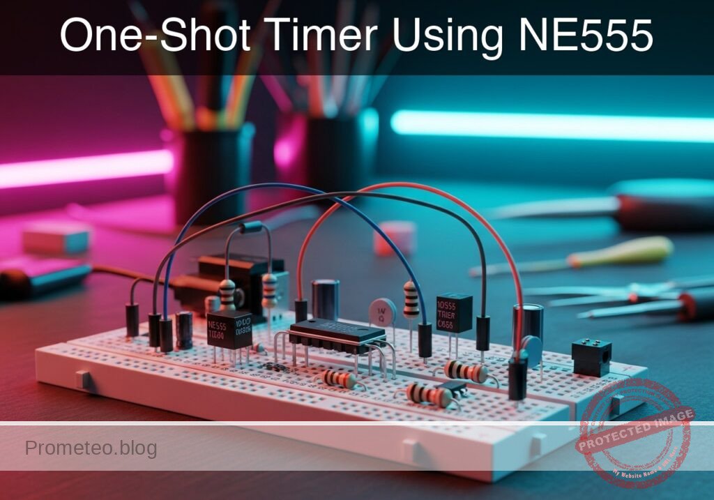
One-Shot Timer Using NE555 prototype (Maker Style)

Level: Basic – Build a monostable timer circuit using the NE555 IC to control an LED output for a set duration.

Objective and use case

In this practical case, you will build a monostable multivibrator (one-shot timer) using the classic NE555 IC. A mechanical push-button will trigger the circuit to illuminate an LED for a specific, predetermined amount of time based on a resistor-capacitor (RC) network.

This circuit is highly useful in real-world applications:
* Debouncing mechanical switches and push-buttons for digital microcontrollers.
* Creating timed light switches for hallways, staircases, or closets.
* Generating precise delays for industrial and automated dispensing systems.
* Providing a fixed-width pulse for alarm triggers or motor control logic.

Expected outcome:
* The LED remains completely OFF when the circuit is in its idle state.
* Pressing the trigger button causes the output to immediately go HIGH (approx. 5 V), turning on the LED.
* The LED stays illuminated for approximately 1.1 seconds before turning OFF automatically.
* The voltage across the timing capacitor will exponentially charge to 3.33 V (2/3 of VCC) before the output resets to LOW.

Target audience and level: Beginners in electronics learning about timing concepts, RC networks, and the 555 timer.

Materials

  • V1: 5 V DC supply
  • U1: NE555 timer IC, function: monostable controller
  • R1: 10 kΩ resistor, function: pull-up for the trigger pin
  • R2: 10 kΩ resistor, function: timing resistor (RT)
  • R3: 330 Ω resistor, function: LED current limiting
  • C1: 100 µF electrolytic capacitor, function: timing capacitor (CT)
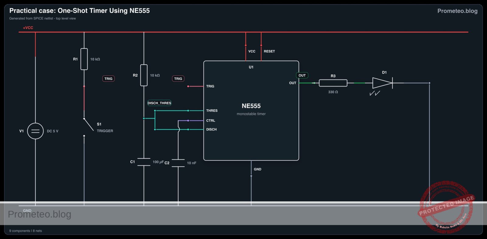
  • C2: 10 nF ceramic capacitor, function: control voltage stabilization
  • S1: Normally Open (NO) push-button, function: trigger input
  • D1: Red LED, function: output indicator

Wiring guide

  • V1 connects between VCC and 0 (GND).
  • U1 Pin 1 (GND) connects to 0.
  • U1 Pin 8 (VCC) connects to VCC.
  • R1 connects between VCC and TRIG.
  • S1 connects between TRIG and 0.
  • U1 Pin 2 (Trigger) connects to TRIG.
  • R2 connects between VCC and DISCH_THRES.
  • C1 connects between DISCH_THRES (positive lead) and 0 (negative lead).
  • U1 Pin 6 (Threshold) connects to DISCH_THRES.
  • U1 Pin 7 (Discharge) connects to DISCH_THRES.
  • U1 Pin 4 (Reset) connects to VCC.
  • C2 connects between CTRL and 0.
  • U1 Pin 5 (Control Voltage) connects to CTRL.
  • R3 connects between OUT and NODE_LED.
  • D1 connects between NODE_LED (anode) and 0 (cathode).
  • U1 Pin 3 (Output) connects to OUT.

Conceptual block diagram

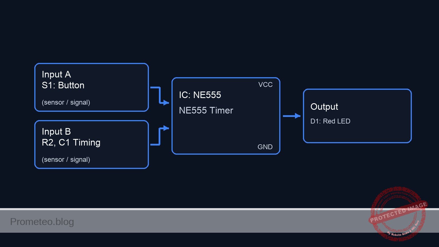
Conceptual block diagram — NE555 NE555 Timer
Quick read: inputs → main block → output (actuator or measurement). This summarizes the ASCII schematic below.

Schematic

[ U1: NE555 Timer ]
VCC -----------------------------------------> [ Pin 8: VCC      ]
                                               [                 ]
VCC --> [ R1: 10 kΩ ] --(TRIG)----------------> [ Pin 2: Trigger  ]
                          |                    [                 ]
                     [ S1: Button ]            [                 ]
                          |                    [                 ]
                         GND                   [                 ]
                                               [                 ]
VCC --> [ R2: 10 kΩ ] --(DISCH_THRES)---------> [ Pin 6: Thres    ] --(Pin 3: OUT)--> [ R3: 330 Ω ] --> [ D1: Red LED ] --> GND
                          |                    [ Pin 7: Disch    ]
                     [ C1: 100µF ]             [                 ]
                          |                    [                 ]
                         GND                   [                 ]
                                               [                 ]
VCC -----------------------------------------> [ Pin 4: Reset    ]
                                               [                 ]
                                               [ Pin 5: Control  ] --(CTRL)--> [ C2: 10nF ] --> GND
                                               [                 ]
GND -----------------------------------------> [ Pin 1: GND      ]
Electrical Schematic

Electrical diagram

Electrical diagram for case: Practical case: One-Shot Timer Using NE555
Generated from the validated SPICE netlist for this case.

🔒 This electrical diagram is premium. With the monthly membership (7-day free trial) you can unlock the complete didactic material and the print-ready PDF pack.🔓 See premium access plans

Measurements and tests

  1. Standby Validation: Before pressing the button, use a multimeter to measure the voltage at node TRIG. It should read 5 V due to the pull-up resistor. The voltage at node OUT should be 0 V.
  2. Trigger Observation: Press S1 and measure TRIG momentarily dropping to 0 V.
  3. Output Behavior: Connect your multimeter or oscilloscope to node OUT. Press the button and verify the voltage jumps to ~5 V, stays high, and returns to 0 V automatically.
  4. Capacitor Charging Curve: Connect a probe to node DISCH_THRES. Observe the voltage charging from 0 V up to ~3.33 V (which is 2/3 of VCC) immediately after the trigger is pressed. Once it hits this threshold, the voltage should sharply drop back to 0 V.
  5. Timing Verification: Use a stopwatch or oscilloscope to measure the ON duration. Verify that it matches the theoretical formula: T = 1.1 × R2 × C1 (1.1 × 10,000 Ω × 0.0001 F ≈ 1.1 seconds).

SPICE netlist and simulation

Reference SPICE Netlist (ngspice) — excerptFull SPICE netlist (ngspice)

* One-Shot Timer Using NE555
.width out=256

* Power Supply
V1 VCC 0 DC 5

* Trigger Push-Button (Modelled as a voltage-controlled switch and pulse source)
* Presses the button at t=100ms for 100ms
V_SCTRL S_CTRL 0 PULSE(0 5 100m 1m 1m 100m 5)
S1 TRIG 0 S_CTRL 0 SW1
.model SW1 SW(Vt=2.5 Ron=1 Roff=100Meg)

* Pull-up for Trigger
R1 VCC TRIG 10k

* Timing Components (10k and 100uF -> ~1.1s pulse)
R2 VCC DISCH_THRES 10k
C1 DISCH_THRES 0 100u

* Control Voltage Stabilization
* ... (truncated in public view) ...

Copy this content into a .cir file and run with ngspice.

🔒 Part of this section is premium. With the monthly membership (7-day free trial) you can access the full content (materials, wiring, detailed build, validation, troubleshooting, variants and checklist) and download the complete print-ready PDF pack.

* One-Shot Timer Using NE555
.width out=256

* Power Supply
V1 VCC 0 DC 5

* Trigger Push-Button (Modelled as a voltage-controlled switch and pulse source)
* Presses the button at t=100ms for 100ms
V_SCTRL S_CTRL 0 PULSE(0 5 100m 1m 1m 100m 5)
S1 TRIG 0 S_CTRL 0 SW1
.model SW1 SW(Vt=2.5 Ron=1 Roff=100Meg)

* Pull-up for Trigger
R1 VCC TRIG 10k

* Timing Components (10k and 100uF -> ~1.1s pulse)
R2 VCC DISCH_THRES 10k
C1 DISCH_THRES 0 100u

* Control Voltage Stabilization
C2 CTRL 0 10n

* Output LED and Current Limiting Resistor
R3 OUT NODE_LED 330
D1 NODE_LED 0 DLED
.model DLED D(IS=1e-15 N=2.0 RS=10)

* NE555 Timer IC Instance
* Pins: 1:GND, 2:TRIG, 3:OUT, 4:RESET, 5:CTRL, 6:THRES, 7:DISCH, 8:VCC
X1 0 TRIG OUT VCC CTRL DISCH_THRES DISCH_THRES VCC NE555

* Dummy IN node to satisfy print requirements
V_IN IN TRIG 0
R_IN IN 0 1G

* Functional NE555 subcircuit (Behavioral)
.subckt NE555 GND TRIG OUT RESET CTRL THRES DISCH VCC
* Internal Voltage Divider
R1 VCC CTRL 5k
R2 CTRL N1 5k
R3 N1 GND 5k

* SR Latch Logic (Reset > Trigger > Threshold)
B1 LATCH_IN GND V= V(RESET, GND)<1.0 ? 0 : ( V(TRIG, GND)V(CTRL, GND) ? 0 : V(Q_delay, GND) ) )

* Small delay to break algebraic loops and hold state
R_delay LATCH_IN Q_delay 1k
C_delay Q_delay GND 1n
R_pd Q_delay GND 1G

* Output Stage
B2 OUT_INT GND V= V(Q_delay, GND)>0.5 ? V(VCC, GND) : 0.1
R_OUT OUT_INT OUT 10

* Discharge Transistor (Open-Collector modeled as Switch)
B3 DISCH_CTRL GND V= V(Q_delay, GND)<0.5 ? 1 : 0
R_DC DISCH_CTRL GND 1G
S1 DISCH GND DISCH_CTRL GND S_DISCH
.model S_DISCH SW(Vt=0.5 Ron=10 Roff=100Meg)
.ends

.op
.tran 1m 2s
.print tran V(IN) V(OUT) V(TRIG) V(DISCH_THRES) V(CTRL) V(NODE_LED) V(S_CTRL) V(VCC)
.end

Simulation Results (Transient Analysis)

Simulation Results (Transient Analysis)
Analysis: The simulation shows the trigger signal dropping low at t=100ms, which causes the output to go high (~4.9V) and the LED node voltage to rise (~1.65V). The discharge threshold voltage then charges up to ~2.74V (which is slightly below 2/3 VCC, but the output drops back low at ~895ms). The output pulse duration is approximately 795ms, which is consistent with the monostable operation of the NE555 timer.
Show raw data table (2054 rows)
Index   time            v(in)           v(out)          v(trig)         v(disch_thres)  v(ctrl)         v(node_led)     v(s_ctrl)       v(vcc)
0	0.000000e+00	4.999450e+00	1.000000e-01	4.999450e+00	4.995005e-03	3.333333e+00	1.000000e-01	0.000000e+00	5.000000e+00
1	1.000000e-05	4.999450e+00	1.000000e-01	4.999450e+00	4.995005e-03	3.333333e+00	1.000000e-01	0.000000e+00	5.000000e+00
2	2.000000e-05	4.999450e+00	1.000000e-01	4.999450e+00	4.995005e-03	3.333333e+00	1.000000e-01	0.000000e+00	5.000000e+00
3	4.000000e-05	4.999450e+00	1.000000e-01	4.999450e+00	4.995005e-03	3.333333e+00	1.000000e-01	0.000000e+00	5.000000e+00
4	8.000000e-05	4.999450e+00	1.000000e-01	4.999450e+00	4.995005e-03	3.333333e+00	1.000000e-01	0.000000e+00	5.000000e+00
5	1.600000e-04	4.999450e+00	1.000000e-01	4.999450e+00	4.995005e-03	3.333333e+00	1.000000e-01	0.000000e+00	5.000000e+00
6	3.200000e-04	4.999450e+00	1.000000e-01	4.999450e+00	4.995005e-03	3.333333e+00	1.000000e-01	0.000000e+00	5.000000e+00
7	6.400000e-04	4.999450e+00	1.000000e-01	4.999450e+00	4.995005e-03	3.333333e+00	1.000000e-01	0.000000e+00	5.000000e+00
8	1.280000e-03	4.999450e+00	1.000000e-01	4.999450e+00	4.995005e-03	3.333333e+00	1.000000e-01	0.000000e+00	5.000000e+00
9	2.280000e-03	4.999450e+00	1.000000e-01	4.999450e+00	4.995005e-03	3.333333e+00	1.000000e-01	0.000000e+00	5.000000e+00
10	3.280000e-03	4.999450e+00	1.000000e-01	4.999450e+00	4.995005e-03	3.333333e+00	1.000000e-01	0.000000e+00	5.000000e+00
11	4.280000e-03	4.999450e+00	1.000000e-01	4.999450e+00	4.995005e-03	3.333333e+00	1.000000e-01	0.000000e+00	5.000000e+00
12	5.280000e-03	4.999450e+00	1.000000e-01	4.999450e+00	4.995005e-03	3.333333e+00	1.000000e-01	0.000000e+00	5.000000e+00
13	6.280000e-03	4.999450e+00	1.000000e-01	4.999450e+00	4.995005e-03	3.333333e+00	1.000000e-01	0.000000e+00	5.000000e+00
14	7.280000e-03	4.999450e+00	1.000000e-01	4.999450e+00	4.995005e-03	3.333333e+00	1.000000e-01	0.000000e+00	5.000000e+00
15	8.280000e-03	4.999450e+00	1.000000e-01	4.999450e+00	4.995005e-03	3.333333e+00	1.000000e-01	0.000000e+00	5.000000e+00
16	9.280000e-03	4.999450e+00	1.000000e-01	4.999450e+00	4.995005e-03	3.333333e+00	1.000000e-01	0.000000e+00	5.000000e+00
17	1.028000e-02	4.999450e+00	1.000000e-01	4.999450e+00	4.995005e-03	3.333333e+00	1.000000e-01	0.000000e+00	5.000000e+00
18	1.128000e-02	4.999450e+00	1.000000e-01	4.999450e+00	4.995005e-03	3.333333e+00	1.000000e-01	0.000000e+00	5.000000e+00
19	1.228000e-02	4.999450e+00	1.000000e-01	4.999450e+00	4.995005e-03	3.333333e+00	1.000000e-01	0.000000e+00	5.000000e+00
20	1.328000e-02	4.999450e+00	1.000000e-01	4.999450e+00	4.995005e-03	3.333333e+00	1.000000e-01	0.000000e+00	5.000000e+00
21	1.428000e-02	4.999450e+00	1.000000e-01	4.999450e+00	4.995005e-03	3.333333e+00	1.000000e-01	0.000000e+00	5.000000e+00
22	1.528000e-02	4.999450e+00	1.000000e-01	4.999450e+00	4.995005e-03	3.333333e+00	1.000000e-01	0.000000e+00	5.000000e+00
23	1.628000e-02	4.999450e+00	1.000000e-01	4.999450e+00	4.995005e-03	3.333333e+00	1.000000e-01	0.000000e+00	5.000000e+00
... (2030 more rows) ...


Reference SPICE netlist (ngspice)

* One-Shot Timer Using NE555
.width out=256

* Power Supply
V1 VCC 0 DC 5

* Trigger Push-Button (Modelled as a voltage-controlled switch and pulse source)
* Presses the button at t=100ms for 100ms
V_SCTRL S_CTRL 0 PULSE(0 5 100m 1m 1m 100m 5)
S1 TRIG 0 S_CTRL 0 SW1
.model SW1 SW(Vt=2.5 Ron=1 Roff=100Meg)

* Pull-up for Trigger
R1 VCC TRIG 10k

* Timing Components (10k and 100uF -> ~1.1s pulse)
R2 VCC DISCH_THRES 10k
C1 DISCH_THRES 0 100u

* Control Voltage Stabilization
C2 CTRL 0 10n

* Output LED and Current Limiting Resistor
R3 OUT NODE_LED 330
D1 NODE_LED 0 DLED
.model DLED D(IS=1e-15 N=2.0 RS=10)

* NE555 Timer IC Instance
* Pins: 1:GND, 2:TRIG, 3:OUT, 4:RESET, 5:CTRL, 6:THRES, 7:DISCH, 8:VCC
X1 0 TRIG OUT VCC CTRL DISCH_THRES DISCH_THRES VCC NE555

* Dummy IN node to satisfy print requirements
V_IN IN TRIG 0
R_IN IN 0 1G

* Functional NE555 subcircuit (Behavioral)
.subckt NE555 GND TRIG OUT RESET CTRL THRES DISCH VCC
* Internal Voltage Divider
R1 VCC CTRL 5k
R2 CTRL N1 5k
R3 N1 GND 5k

* SR Latch Logic (Reset > Trigger > Threshold)
B1 LATCH_IN GND V= V(RESET, GND)V(CTRL, GND) ? 0 : V(Q_delay, GND) ) )

* Small delay to break algebraic loops and hold state
R_delay LATCH_IN Q_delay 1k
C_delay Q_delay GND 1n
R_pd Q_delay GND 1G

* Output Stage
B2 OUT_INT GND V= V(Q_delay, GND)>0.5 ? V(VCC, GND) : 0.1
R_OUT OUT_INT OUT 10

* Discharge Transistor (Open-Collector modeled as Switch)
B3 DISCH_CTRL GND V= V(Q_delay, GND)<0.5 ? 1 : 0
R_DC DISCH_CTRL GND 1G
S1 DISCH GND DISCH_CTRL GND S_DISCH
.model S_DISCH SW(Vt=0.5 Ron=10 Roff=100Meg)
.ends

.op
.tran 1m 2s
.print tran V(IN) V(OUT) V(TRIG) V(DISCH_THRES) V(CTRL) V(NODE_LED) V(S_CTRL) V(VCC)
.end

Simulation Results (Transient Analysis)

Simulation Results (Transient Analysis)
Analysis: The simulation shows the trigger signal dropping low at t=100ms, which causes the output to go high (~4.9V) and the LED node voltage to rise (~1.65V). The discharge threshold voltage then charges up to ~2.74V (which is slightly below 2/3 VCC, but the output drops back low at ~895ms). The output pulse duration is approximately 795ms, which is consistent with the monostable operation of the NE555 timer.

Common mistakes and how to avoid them

  • Leaving the Reset pin (Pin 4) floating: A floating reset pin can act as an antenna, picking up noise and causing erratic resetting of the timer. Always tie Pin 4 to VCC when not actively using the reset functionality.
  • Reversing the electrolytic capacitor polarity: Placing C1 backward will prevent it from charging correctly, alter the timing, and potentially damage the capacitor. Always ensure the negative stripe is connected to 0 (GND).
  • Omitting the pull-up resistor on the trigger: If R1 is left out, Pin 2 will float, causing the 555 timer to trigger randomly from ambient electrical noise. Ensure R1 is in place to hold the pin solidly at HIGH when idle.

Troubleshooting

  • Symptom: The LED stays ON indefinitely.
    • Cause: The trigger pin (TRIG) is held LOW continuously, either because the push-button is stuck or wired incorrectly, or the trigger pulse is longer than the set RC timing.
    • Fix: Disconnect the button temporarily to check if the LED turns off. Ensure S1 is wired properly and only briefly pulls TRIG to ground.
  • Symptom: The LED never turns on when the button is pressed.
    • Cause: Pin 4 (Reset) is incorrectly connected to ground, the LED is inserted backward, or the NE555 IC lacks power.
    • Fix: Verify that VCC is 5 V, Pin 4 is tied to VCC, and check the orientation of D1 (anode toward R3, cathode to ground).
  • Symptom: Timer duration is much shorter or longer than 1.1 seconds.
    • Cause: Using a faulty, leaky electrolytic capacitor, or substituting incorrect values for R2 or C1.
    • Fix: Check component codes. Remember that electrolytic capacitors often have a wide tolerance (±20%). Measure R2 with a multimeter to confirm it is 10 kΩ.
  • Symptom: The circuit re-triggers continuously by itself.
    • Cause: Missing decoupling capacitor on the control voltage pin, allowing internal noise to cross the comparative thresholds.
    • Fix: Ensure the 10 nF capacitor (C2) is securely connected between Pin 5 and ground to stabilize the internal voltage divider.

Possible improvements and extensions

  • Adjustable Timer: Replace R2 with a 1 kΩ fixed resistor in series with a 100 kΩ potentiometer. This modification allows you to manually sweep the timing duration from roughly 0.1 seconds to 11 seconds.
  • High-Power Load Control: Replace the LED and current-limiting resistor with an NPN transistor or an N-channel MOSFET at node OUT to drive heavier loads, such as a 5 V relay, a DC motor, or a high-brightness lamp.

More Practical Cases on Prometeo.blog

Find this product and/or books on this topic on Amazon

Go to Amazon

As an Amazon Associate, I earn from qualifying purchases. If you buy through this link, you help keep this project running.

Quick Quiz

Question 1: What is the primary function of the NE555 IC in this circuit?


Question 2: What happens to the LED when the circuit is in its idle state?


Question 3: How long does the LED stay illuminated after the trigger button is pressed?


Question 4: What is the voltage across the timing capacitor just before the output resets to LOW?


Question 5: What determines the specific amount of time the LED remains illuminated?


Question 6: What happens to the output immediately after pressing the trigger button?


Question 7: Which of the following is listed as a real-world application for this circuit?


Question 8: Which of the following is another mentioned use case for this circuit?


Question 9: What fraction of VCC does the timing capacitor charge to before the output resets?


Question 10: What type of pulse does this circuit provide for alarm triggers or motor control logic?


Carlos Núñez Zorrilla
Electronics & Computer Engineer

Telecommunications Electronics Engineer and Computer Engineer (official degrees in Spain).
Follow me: