Level: Medium – Demonstrate the high impedance of the inductor at high frequencies to block noise in power lines.
Objective and use case
You will construct an LR low-pass filter using an RF choke to isolate a DC power line from high-frequency AC noise. By superimposing an AC signal onto a DC voltage supply, you will observe how the inductor’s frequency-dependent reactance permits DC to pass while heavily attenuating high-frequency noise before it reaches the load.
This circuit concept is highly useful in the real world for:
* Preventing high-frequency switching noise from entering sensitive analog sensor circuits.
* Filtering out radio frequency interference (RFI) from long power supply lines.
* Isolating different functional blocks that share a common power rail on a PCB.
* Protecting automotive audio and communication electronics from alternator whine.
Expected outcome:
* The mixed input signal (V_IN_MIX) will display a steady DC offset combined with significant high-frequency ripples.
* The output voltage (V_OUT_CLEAN) across the load will show a stable DC level with the AC noise vastly reduced.
* An FFT (Fast Fourier Transform) analysis of the input will reveal a large 0 Hz (DC) component and a prominent high-frequency peak.
* An FFT analysis of the output will show the high-frequency peak almost completely suppressed, confirming the choke’s blocking action.
Target audience: Intermediate electronics students learning about reactive components and AC/DC superimposition.
Materials
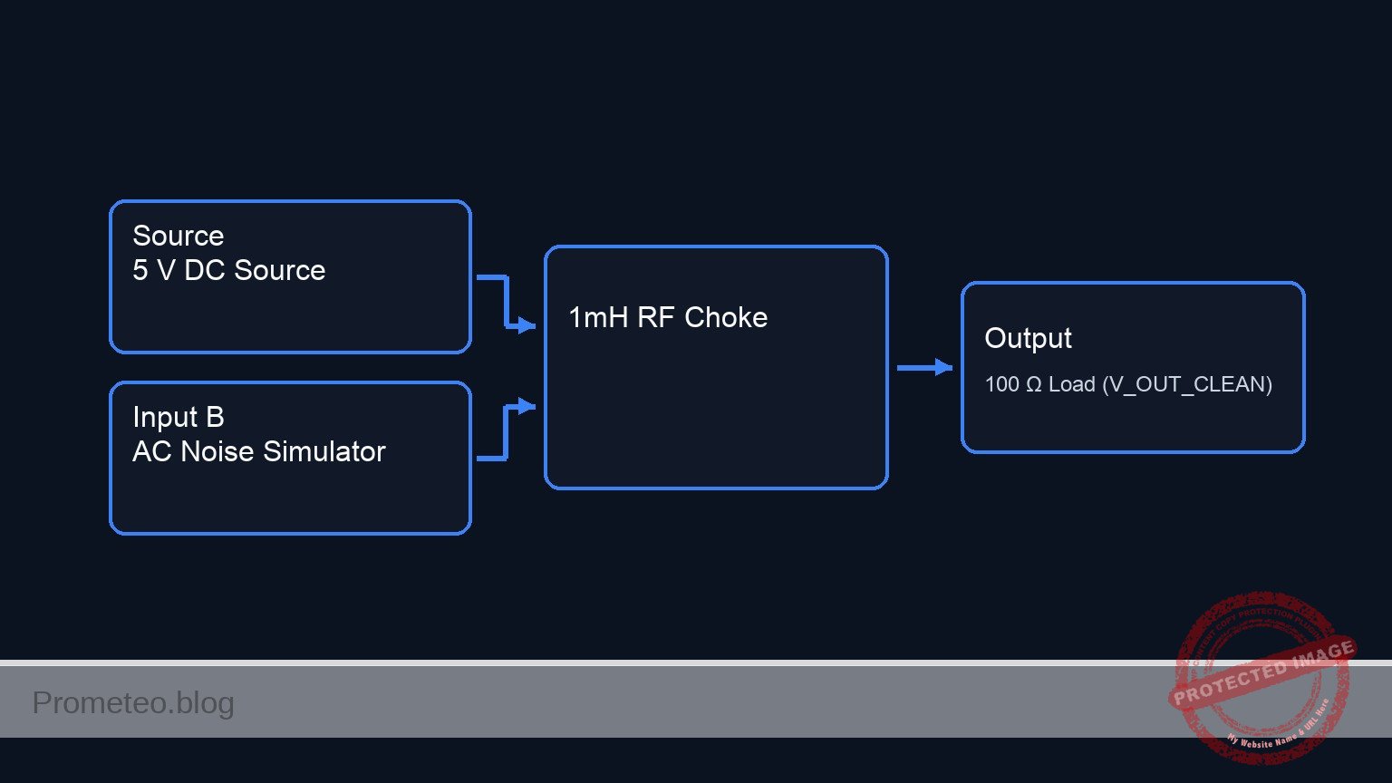
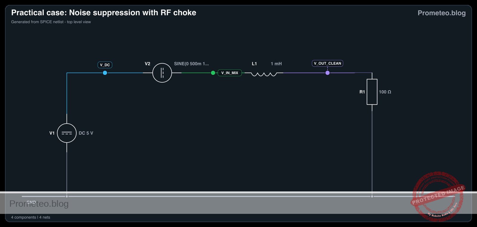
- V1: 5 V DC source, function: main DC power supply
- V2: 500 mV peak sine wave AC source at 100 kHz, function: high-frequency noise simulator
- L1: 1 mH inductor, function: RF choke to block high-frequency noise
- R1: 100 Ω resistor, function: load simulation
Wiring guide
- V1: connects between V_DC and 0
- V2: connects between V_IN_MIX and V_DC
- L1: connects between V_IN_MIX and V_OUT_CLEAN
- R1: connects between V_OUT_CLEAN and 0
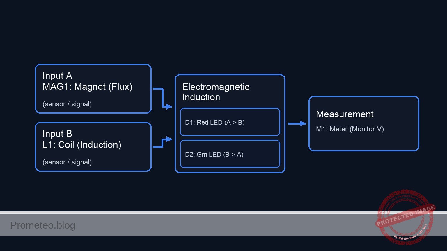
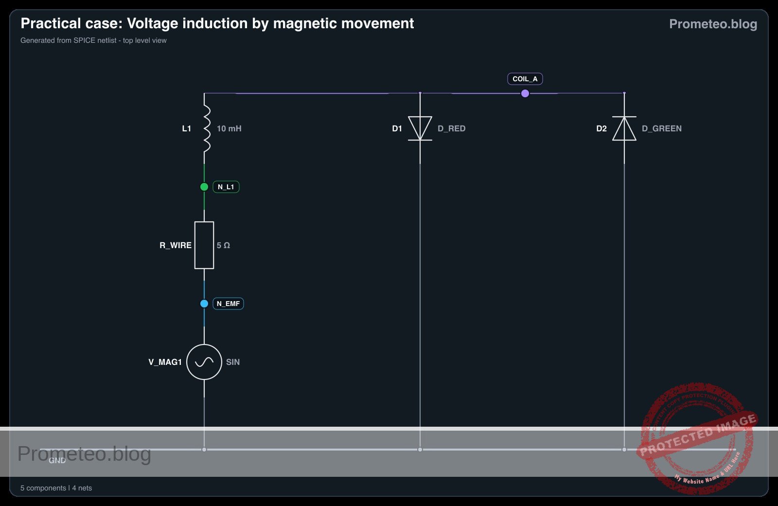
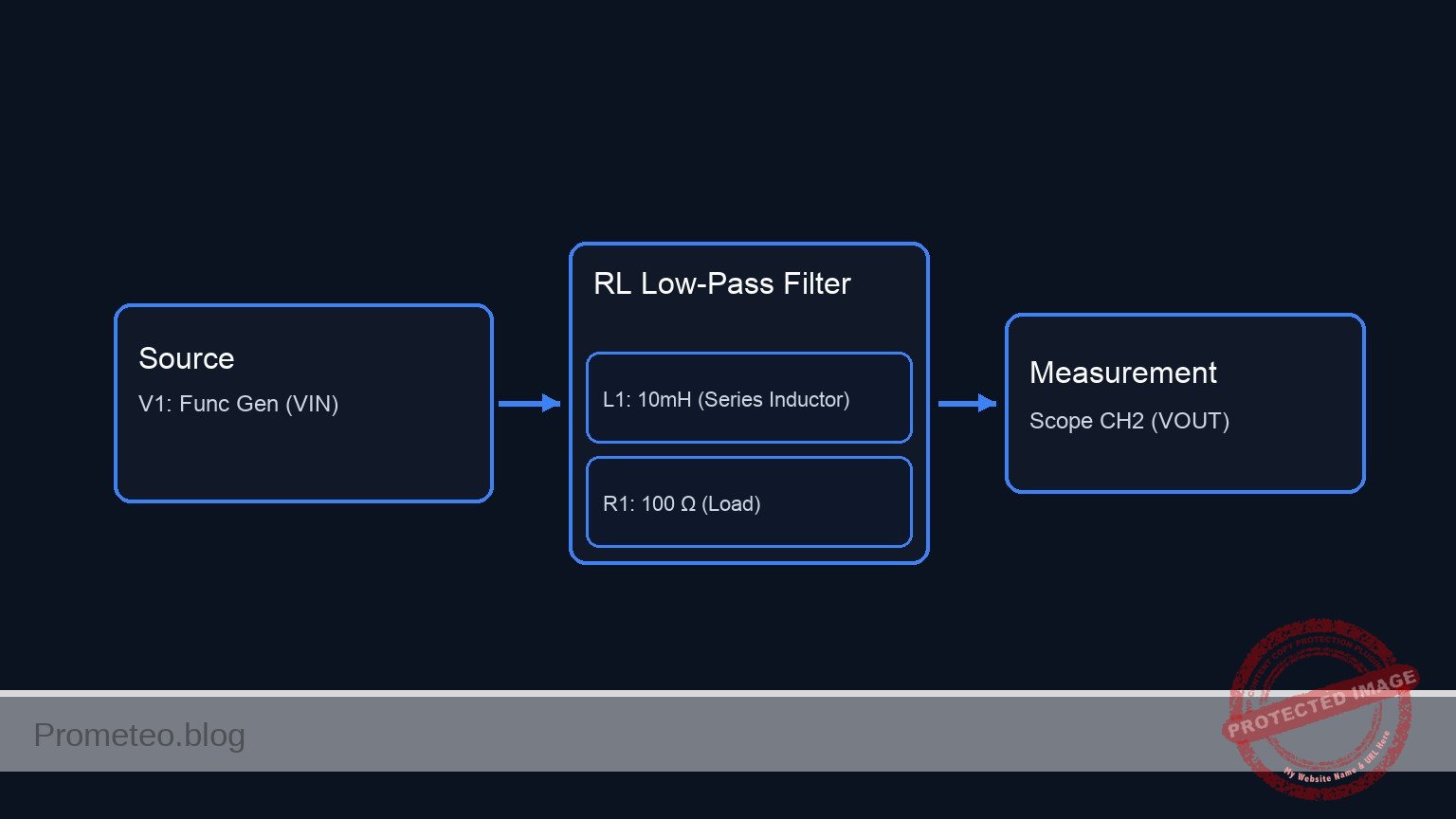
Conceptual block diagram
Schematic
[ V1: 5 V DC Source ] --(V_DC)--> [ V2: AC Noise Simulator ] --(V_IN_MIX)--> [ L1: 1mH RF Choke ] --(V_OUT_CLEAN)--> [ R1: 100 Ω Load ] --> GND
Electrical diagram
Measurements and tests
- Connect an oscilloscope probe to V_IN_MIX with the ground clip attached to node 0. Set the channel coupling to DC. You should observe a 5 V DC baseline with a 1 V peak-to-peak 100 kHz sine wave riding on top of it.
- Connect a second oscilloscope probe to V_OUT_CLEAN. Observe that the DC voltage remains at approximately 5 V, but the high-frequency 100 kHz ripple is drastically attenuated due to the high inductive reactance (XL = 2\pi fL) of the choke.
- Activate the FFT (Fast Fourier Transform) math function on the oscilloscope for the V_IN_MIX channel. Note the massive spike at 0 Hz (representing the 5 V DC component) and the distinct noise spike at 100 kHz.
- Apply the FFT function to the V_OUT_CLEAN channel. Compare the magnitude of the 100 kHz spike against the input measurement; it should be significantly reduced, successfully proving the inductor’s high-frequency blocking capabilities.
SPICE netlist and simulation
Reference SPICE Netlist (ngspice) — excerptFull SPICE netlist (ngspice)
* Noise suppression with RF choke
.width out=256

* Main DC power supply (5V)
V1 V_DC 0 DC 5

* High-frequency noise simulator (500mV peak, 100kHz sine wave superimposed on DC)
V2 V_IN_MIX V_DC SINE(0 500m 100k)

* RF choke to block high-frequency noise (1mH)
L1 V_IN_MIX V_OUT_CLEAN 1m

* Load simulation (100 ohms)
* ... (truncated in public view) ...
Copy this content into a .cir file and run with ngspice.
* Noise suppression with RF choke
.width out=256

* Main DC power supply (5V)
V1 V_DC 0 DC 5

* High-frequency noise simulator (500mV peak, 100kHz sine wave superimposed on DC)
V2 V_IN_MIX V_DC SINE(0 500m 100k)

* RF choke to block high-frequency noise (1mH)
L1 V_IN_MIX V_OUT_CLEAN 1m

* Load simulation (100 ohms)
R1 V_OUT_CLEAN 0 100

* Analysis directives
.op
* Simulate for 100us to capture 10 full cycles of the 100kHz noise
.tran 0.1u 100u
.print tran V(V_IN_MIX) V(V_OUT_CLEAN) V(V_DC) I(L1)

.end
Simulation Results (Transient Analysis)

Show raw data table (1008 rows)
Index   time            v(v_in_mix)     v(v_out_clean)  v(v_dc)         l1#branch
0	0.000000e+00	5.000000e+00	5.000000e+00	5.000000e+00	5.000000e-02
1	1.000000e-09	5.000314e+00	5.000000e+00	5.000000e+00	5.000000e-02
2	2.000000e-09	5.000628e+00	5.000000e+00	5.000000e+00	5.000000e-02
3	4.000000e-09	5.001257e+00	5.000000e+00	5.000000e+00	5.000000e-02
4	8.000000e-09	5.002513e+00	5.000001e+00	5.000000e+00	5.000001e-02
5	1.600000e-08	5.005026e+00	5.000004e+00	5.000000e+00	5.000004e-02
6	3.200000e-08	5.010052e+00	5.000016e+00	5.000000e+00	5.000016e-02
7	6.400000e-08	5.020101e+00	5.000064e+00	5.000000e+00	5.000064e-02
8	1.280000e-07	5.040169e+00	5.000256e+00	5.000000e+00	5.000256e-02
9	2.280000e-07	5.071384e+00	5.000808e+00	5.000000e+00	5.000808e-02
10	3.280000e-07	5.102316e+00	5.001665e+00	5.000000e+00	5.001665e-02
11	4.280000e-07	5.132845e+00	5.002818e+00	5.000000e+00	5.002818e-02
12	5.280000e-07	5.162850e+00	5.004261e+00	5.000000e+00	5.004261e-02
13	6.280000e-07	5.192212e+00	5.005985e+00	5.000000e+00	5.005985e-02
14	7.280000e-07	5.220816e+00	5.007980e+00	5.000000e+00	5.007980e-02
15	8.280000e-07	5.248548e+00	5.010236e+00	5.000000e+00	5.010236e-02
16	9.280000e-07	5.275299e+00	5.012741e+00	5.000000e+00	5.012741e-02
17	1.028000e-06	5.300963e+00	5.015481e+00	5.000000e+00	5.015481e-02
18	1.128000e-06	5.325440e+00	5.018443e+00	5.000000e+00	5.018443e-02
19	1.228000e-06	5.348633e+00	5.021613e+00	5.000000e+00	5.021613e-02
20	1.328000e-06	5.370449e+00	5.024976e+00	5.000000e+00	5.024976e-02
21	1.428000e-06	5.390804e+00	5.028515e+00	5.000000e+00	5.028515e-02
22	1.528000e-06	5.409616e+00	5.032213e+00	5.000000e+00	5.032213e-02
23	1.628000e-06	5.426812e+00	5.036054e+00	5.000000e+00	5.036054e-02
... (984 more rows) ...
Reference SPICE netlist (ngspice)
* Noise suppression with RF choke
.width out=256

* Main DC power supply (5V)
V1 V_DC 0 DC 5

* High-frequency noise simulator (500mV peak, 100kHz sine wave superimposed on DC)
V2 V_IN_MIX V_DC SINE(0 500m 100k)

* RF choke to block high-frequency noise (1mH)
L1 V_IN_MIX V_OUT_CLEAN 1m

* Load simulation (100 ohms)
R1 V_OUT_CLEAN 0 100

* Analysis directives
.op
* Simulate for 100us to capture 10 full cycles of the 100kHz noise
.tran 0.1u 100u
.print tran V(V_IN_MIX) V(V_OUT_CLEAN) V(V_DC) I(L1)

.end
Simulation Results (Transient Analysis)
Common mistakes and how to avoid them
- Using an inductor with a low self-resonant frequency (SRF): All inductors have parasitic winding capacitance. If the noise frequency exceeds the inductor’s SRF, the component behaves like a capacitor and allows high-frequency noise to pass straight through. Always verify the SRF is well above your target noise frequency.
- Neglecting the inductor’s DC resistance (DCR): Inductors are made of coiled wire which naturally possesses resistance. High load currents passing through an inductor with high DCR will cause an unacceptable DC voltage drop. Choose a choke with an appropriately low DCR for your load.
- Core saturation due to high DC current: If the load draws more continuous current than the inductor’s saturation rating (Isat), the core’s magnetic flux saturates. This causes the inductance to drop sharply, destroying its filtering capability. Always check the saturation current rating.
Troubleshooting
- Symptom: High-frequency noise is still heavily present at V_OUT_CLEAN.
- Cause: The inductor value is too low to provide significant reactance at the simulated noise frequency, or its SRF has been exceeded.
- Fix: Increase the inductance value (e.g., scale from 10 µH to 1 mH) or verify the frequency limits of the specific choke being used.
- Symptom: Significant DC voltage drop at V_OUT_CLEAN under load (e.g., reading 4 V instead of 5 V).
- Cause: The inductor’s internal DC resistance (DCR) is too high relative to the load resistor R1.
- Fix: Replace the inductor with a physically larger one that uses thicker wire, which lowers the DCR, or increase the load resistance if it’s drawing more current than intended.
- Symptom: The choke gets excessively hot during operation.
- Cause: The DC current drawn by the load exceeds the continuous thermal current rating (Irms) of the inductor.
- Fix: Select a higher-rated power inductor capable of safely handling the steady-state load current.
Possible improvements and extensions
- Form an LC Low-Pass Filter: Add a decoupling capacitor (e.g., 100 nF or 1 µF) parallel to the load (between V_OUT_CLEAN and 0). This creates a second-order filter, providing a much steeper roll-off and vastly superior noise attenuation compared to the simple LR configuration.
- Implement a Pi-Filter: Use a Capacitor-Inductor-Capacitor (C-L-C) arrangement to provide bidirectional noise suppression. This not only cleans the power entering the load but also prevents any switching noise generated by the load from polluting the main DC supply line.
More Practical Cases on Prometeo.blog
Find this product and/or books on this topic on Amazon
As an Amazon Associate, I earn from qualifying purchases. If you buy through this link, you help keep this project running.
Quick Quiz

Telecommunications Electronics Engineer and Computer Engineer (official degrees in Spain).