Level: Medium – Use a very low-value resistor to indirectly measure a DC load’s current via voltage drop.
Objective and use case
You will build a direct current (DC) circuit featuring a primary dummy load and a low-value series resistor, known as a shunt. By measuring the tiny voltage drop across this shunt, you will indirectly calculate the total current flowing through the circuit using Ohm’s Law.
Why this is useful:
* Safe high-current measurement: Avoids running massive currents directly through your multimeter’s internal, potentially fragile, circuitry.
* Continuous monitoring: Allows microcontrollers or analog panels to constantly track power consumption without breaking the circuit.
* Overcurrent protection: Provides a proportional voltage signal that can trigger a shutdown mechanism if the current exceeds safe limits.
* Lowering burden voltage: Customizing the shunt size minimizes the interference the measurement instrument imposes on the operating circuit.
Expected outcome:
* You will generate a measurable millivolt-range voltage drop across the low-side shunt resistor.
* You will correctly calculate the load current ($I = V/R$) from the observed voltage.
* You will verify the power dissipation (P = I^2 × R) of the shunt to ensure it operates within safe thermal limits.
Target audience and level: Intermediate electronics students learning indirect measurement techniques and power calculations.
Materials
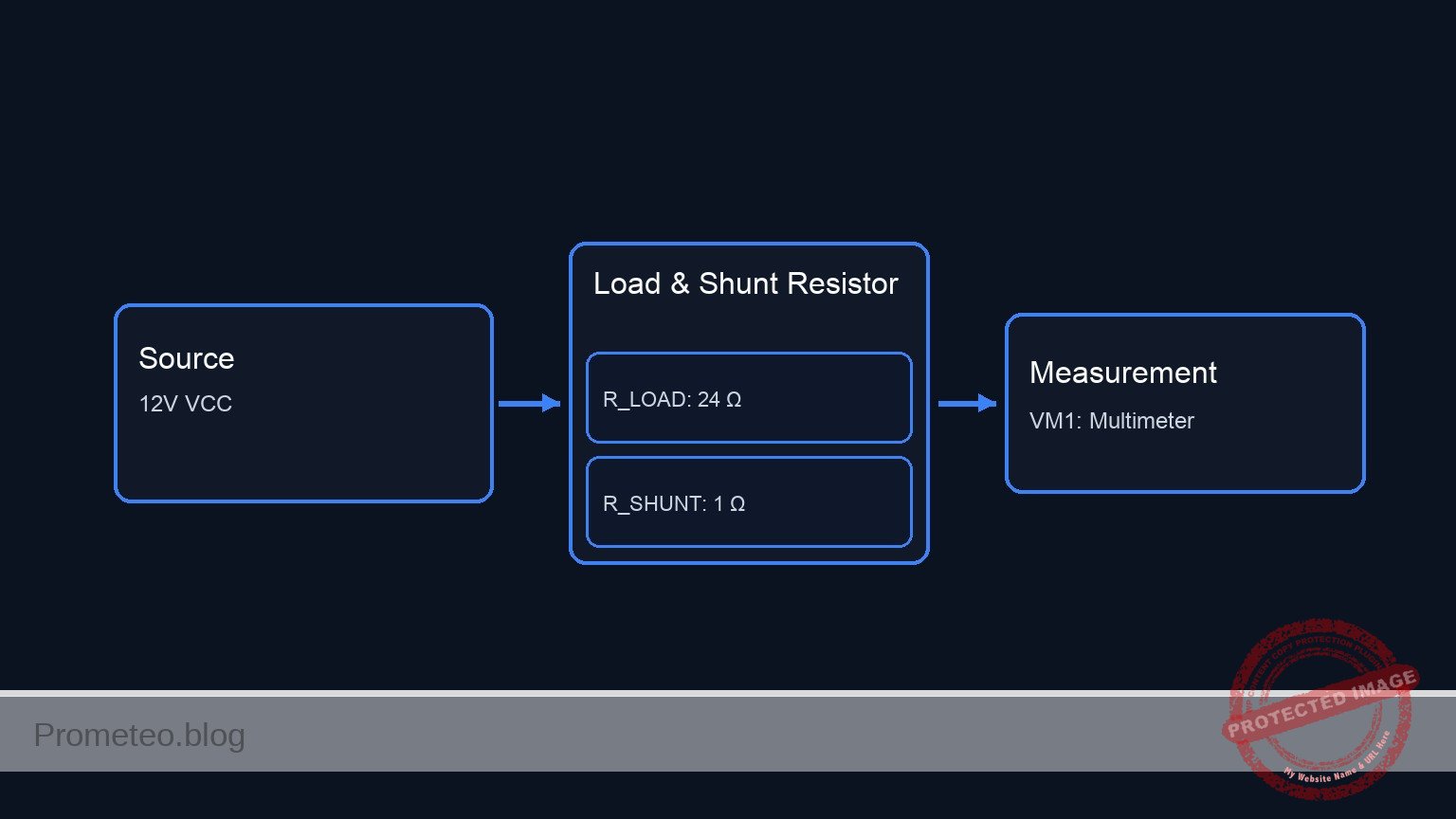
V1: 12 V DC supply, function: main power sourceR_LOAD: 24 Ω resistor (10 W), function: primary DC loadR_SHUNT: 1 Ω resistor (1 W), function: current sensing shuntVM1: Digital Multimeter, function: measure voltage drop across shunt
Wiring guide
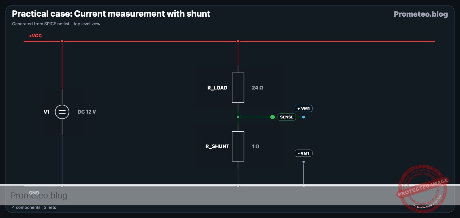
V1: connects positive terminal to nodeVCCand negative terminal to node0(GND).R_LOAD: connects between nodeVCCand nodeSENSE.R_SHUNT: connects between nodeSENSEand node0(GND).VM1: connects positive probe to nodeSENSEand negative probe to node0(GND) to measure the voltage drop across the shunt.
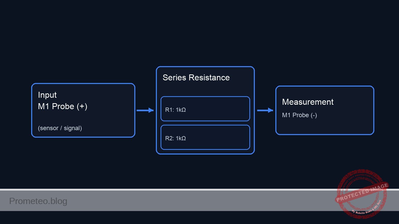
Conceptual block diagram
Schematic
[ V1: 12 V VCC ] --> [ R_LOAD: 24 Ω ] --(Node SENSE)--> [ R_SHUNT: 1 Ω ] --> GND
                                           |
                                           +--(+ probe)--> [ VM1: Multimeter ] --(- probe)--> GND
Electrical diagram
Measurements and tests
- Verify the power supply: Turn on
V1and measure the voltage at nodeVCCrelative to node0. It should read exactly 12 V. - Measure the shunt voltage (Vshunt): Set your multimeter to the DC millivolts or volts range. Measure the voltage at node
SENSErelative to node0. With a 24 Ω load and a 1 Ω shunt (25 Ω total), you should measure approximately 480 mV (0.48 V). - Calculate the current: Use Ohm’s law (I = Vshunt / Rshunt). Divide the 0.48 V measurement by 1 Ω. The total current flowing through the circuit is 480 mA (0.48 A).
- Calculate power dissipation: Calculate the power dissipated by the shunt using P = Vshunt × I. In this case, 0.48 V × 0.48 A = 0.23 W. Because we selected a 1 W resistor, it is operating safely within its limits.
- Measure load voltage drop: Measure the voltage between node
VCCand nodeSENSE. It should be approximately 11.52 V, confirming that the shunt «steals» very little voltage from the primary load.
SPICE netlist and simulation
Reference SPICE Netlist (ngspice)
* Practical case: Current measurement with shunt
.width out=256

* Main power source
V1 VCC 0 DC 12

* Primary DC load
R_LOAD VCC SENSE 24

* Current sensing shunt
R_SHUNT SENSE 0 1

* Simulation commands
.op
.tran 1u 100u

* Print the input voltage and the voltage drop across the shunt (VM1)
.print tran V(VCC) V(SENSE)

.end
Copy this content into a .cir file and run with ngspice.
Simulation Results (Transient Analysis)

Show raw data table (108 rows)
Index   time            v(vcc)          v(sense)
0	0.000000e+00	1.200000e+01	4.800000e-01
1	1.000000e-08	1.200000e+01	4.800000e-01
2	2.000000e-08	1.200000e+01	4.800000e-01
3	4.000000e-08	1.200000e+01	4.800000e-01
4	8.000000e-08	1.200000e+01	4.800000e-01
5	1.600000e-07	1.200000e+01	4.800000e-01
6	3.200000e-07	1.200000e+01	4.800000e-01
7	6.400000e-07	1.200000e+01	4.800000e-01
8	1.280000e-06	1.200000e+01	4.800000e-01
9	2.280000e-06	1.200000e+01	4.800000e-01
10	3.280000e-06	1.200000e+01	4.800000e-01
11	4.280000e-06	1.200000e+01	4.800000e-01
12	5.280000e-06	1.200000e+01	4.800000e-01
13	6.280000e-06	1.200000e+01	4.800000e-01
14	7.280000e-06	1.200000e+01	4.800000e-01
15	8.280000e-06	1.200000e+01	4.800000e-01
16	9.280000e-06	1.200000e+01	4.800000e-01
17	1.028000e-05	1.200000e+01	4.800000e-01
18	1.128000e-05	1.200000e+01	4.800000e-01
19	1.228000e-05	1.200000e+01	4.800000e-01
20	1.328000e-05	1.200000e+01	4.800000e-01
21	1.428000e-05	1.200000e+01	4.800000e-01
22	1.528000e-05	1.200000e+01	4.800000e-01
23	1.628000e-05	1.200000e+01	4.800000e-01
... (84 more rows) ...
Reference SPICE netlist (ngspice)
* Practical case: Current measurement with shunt
.width out=256

* Main power source
V1 VCC 0 DC 12

* Primary DC load
R_LOAD VCC SENSE 24

* Current sensing shunt
R_SHUNT SENSE 0 1

* Simulation commands
.op
.tran 1u 100u

* Print the input voltage and the voltage drop across the shunt (VM1)
.print tran V(VCC) V(SENSE)

.end
Simulation Results (Transient Analysis)
Common mistakes and how to avoid them
- Using a shunt with too much resistance: If the shunt value is too high (e.g., 100 Ω), it creates a massive «burden voltage,» starving the actual load of power and altering the circuit’s behavior. Always use low values (typically 1 Ω, 0.1 Ω, or even milliohms).
- Ignoring the power rating of the shunt: A resistor dropping even a fraction of a volt can dissipate substantial heat if the current is high. Always calculate P = I^2 × R and select a resistor with double the calculated wattage rating.
- Measuring current directly across the shunt: Setting the multimeter to «Amps» mode and putting it in parallel with the shunt will short out the shunt, potentially blowing the multimeter’s internal fuse. Always use the «Voltage» mode to measure the voltage drop across the shunt.
Troubleshooting
- Symptom: Multimeter reads 0 V across the shunt.
- Cause: The circuit is open; power isn’t reaching the load, or
R_SHUNTis shorted out. - Fix: Check all wire continuity, ensure the power supply is turned on, and confirm the load is properly connected.
- Cause: The circuit is open; power isn’t reaching the load, or
- Symptom: The shunt resistor is smoking or gets dangerously hot.
- Cause: The current exceeds the wattage rating of the shunt, or
R_LOADhas been bypassed (creating a short circuit directly through the shunt). - Fix: Immediately turn off the power. Verify
R_LOADis not bypassed and replace the shunt with one of a higher wattage rating if necessary.
- Cause: The current exceeds the wattage rating of the shunt, or
- Symptom: The calculated current seems far lower than the expected load consumption.
- Cause: The resistance of the connecting wires or breadboard contacts is acting as an unmeasured secondary shunt, adding to the total circuit resistance.
- Fix: Ensure short, thick wires are used for power connections. Consider switching to a 4-wire (Kelvin) measurement setup for extreme precision.
Possible improvements and extensions
- Add a current-sense amplifier: Connect an Operational Amplifier (Op-Amp) across
R_SHUNTin a non-inverting configuration to amplify the small millivolt signal into a robust 0-5 V signal easily readable by a microcontroller’s ADC. - Implement high-side sensing: Move
R_SHUNTto the «high side» (betweenVCCandR_LOAD). Use a dedicated high-side current sensing IC (such as the INA219) to measure the differential voltage, proving that current can be measured before it reaches the load while keeping the load strictly grounded.
More Practical Cases on Prometeo.blog
Find this product and/or books on this topic on Amazon
As an Amazon Associate, I earn from qualifying purchases. If you buy through this link, you help keep this project running.
Quick Quiz

Telecommunications Electronics Engineer and Computer Engineer (official degrees in Spain).