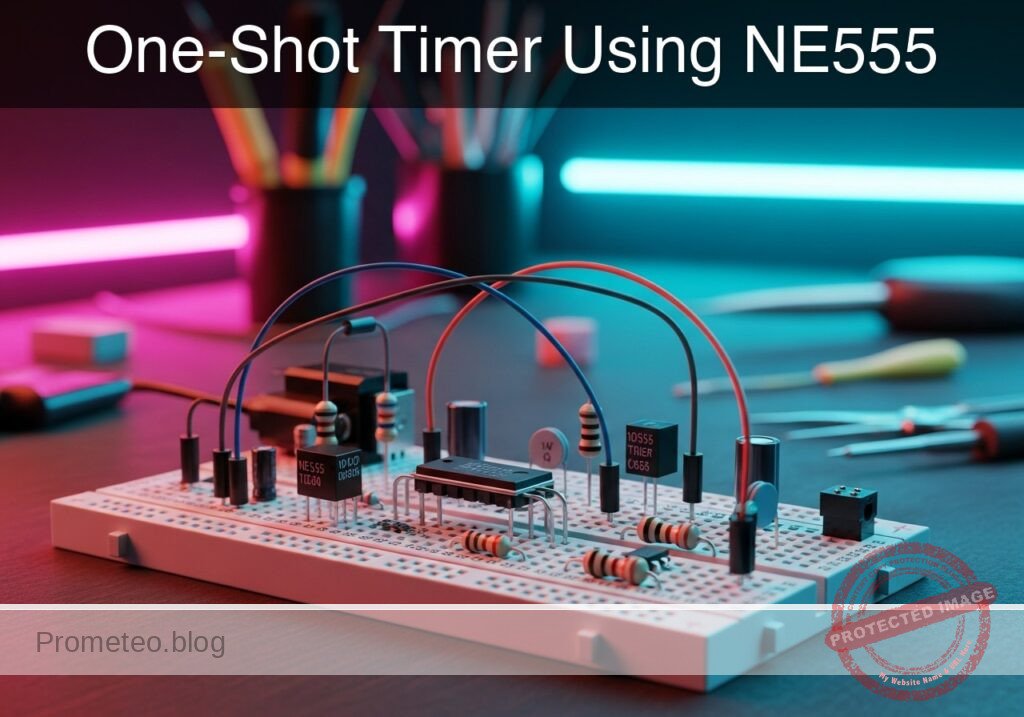
Level: Basic — Build an NE555 astable timer that blinks an LED at a visible frequency.
Objective and use case
You will build a simple astable timer with an NE555 powered from 5 V. The circuit will generate a repetitive square wave that turns an LED on and off continuously.
Why it is useful:
– It demonstrates how a basic timer generates a clock signal without a microcontroller.
– It is useful as a visual blink indicator for power or system status.
– It can be used as a simple test source for checking frequency measurement tools.
– It helps students observe capacitor charge and discharge behavior in a real circuit.
Expected outcome:
– VOUT switches between approximately 0 V and 5 V.
– The LED blinks at a clearly visible rate, about 1 Hz to 3 Hz.
– The timing node TH_TR shows a repeating charge/discharge waveform between about 1/3 VCC and 2/3 VCC.
– The measured period is close to the value predicted by the NE555 astable equations.
– The duty cycle is greater than 50% for the standard RA/RB astable connection.
Target audience and level: Beginners in basic electronics laboratory practice.
Materials
- U1: NE555 timer IC, function: astable oscillator core
- R1: 10 kΩ resistor, function: timing resistor RA from VCC to DIS
- R2: 68 kΩ resistor, function: timing resistor RB from DIS to TH_TR
- C1: 10 µF electrolytic capacitor, function: timing capacitor
- C2: 10 nF capacitor, function: control-voltage noise filter on CV
- C3: 100 nF capacitor, function: supply decoupling across VCC and GND
- R3: 330 Ω resistor, function: LED current limiting
- D1: red LED, function: visual output indicator
- V1: 5 V DC supply
- B1: breadboard, function: circuit assembly platform
- J1: jumper wires, function: interconnections
Wiring guide
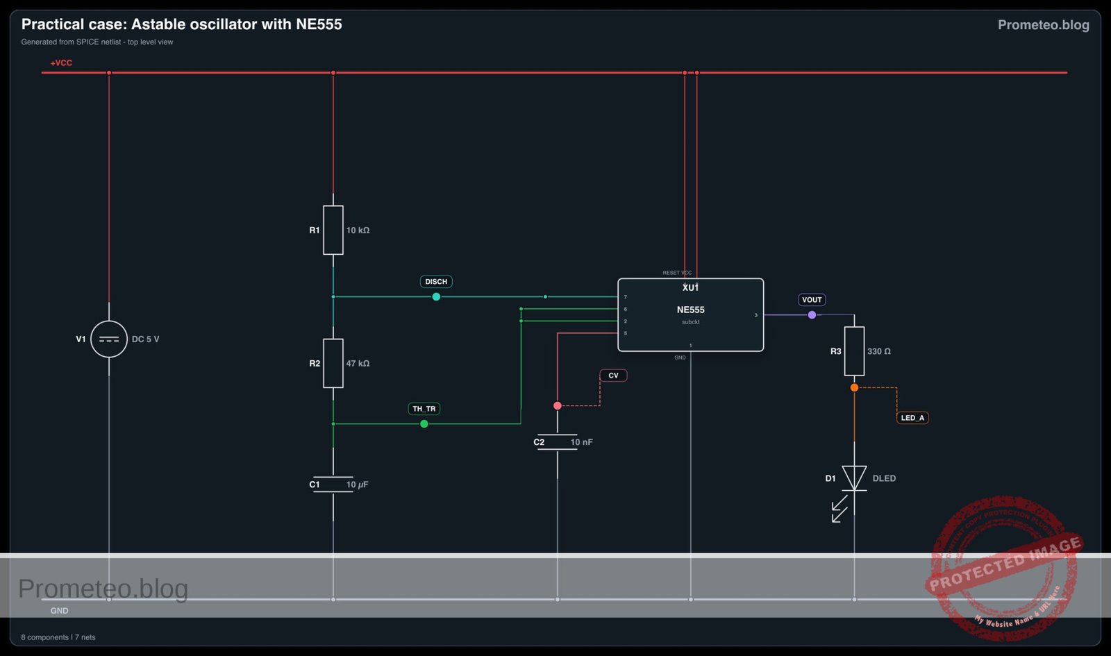
Use the node names VCC, 0, DIS, TH_TR, CV, RESET, and VOUT.
- V1 connects between nodes VCC and 0.
- U1 pin 8 (VCC) connects to node VCC.
- U1 pin 1 (GND) connects to node 0.
- U1 pin 4 (RESET) connects to node VCC.
- U1 pin 3 (OUT) connects to node VOUT.
- U1 pin 7 (DISCH) connects to node DIS.
- U1 pin 2 (TRIG) connects to node TH_TR.
- U1 pin 6 (THRESH) connects to node TH_TR.
- U1 pin 5 (CTRL) connects to node CV.
- R1 connects between nodes VCC and DIS.
- R2 connects between nodes DIS and TH_TR.
- C1 connects between nodes TH_TR and 0; if electrolytic, connect the positive lead to TH_TR and the negative lead to 0.
- C2 connects between nodes CV and 0.
- C3 connects between nodes VCC and 0, placed physically close to U1.
- R3 connects between nodes VOUT and LED_A.
- D1 connects between nodes LED_A and 0; connect the anode to LED_A and the cathode to 0.
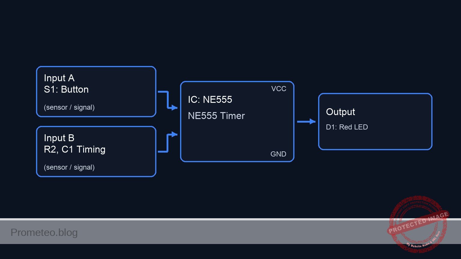
Conceptual block diagram
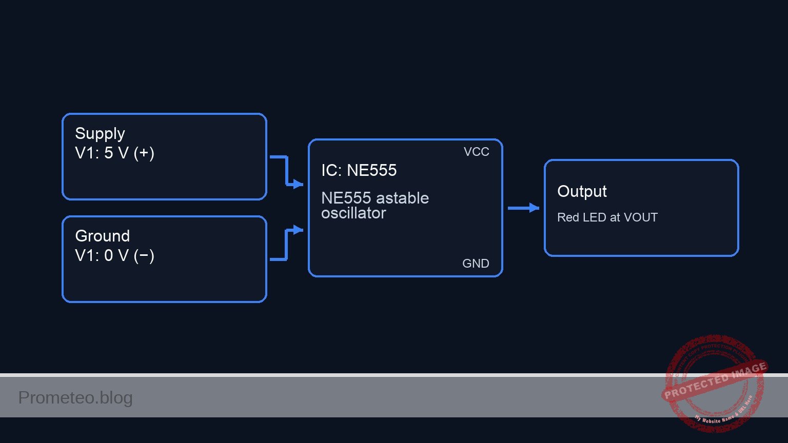
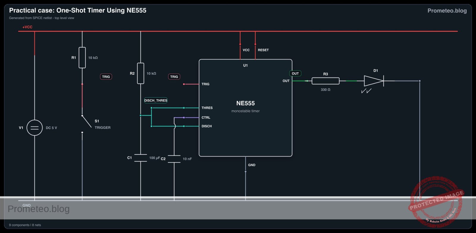
Schematic
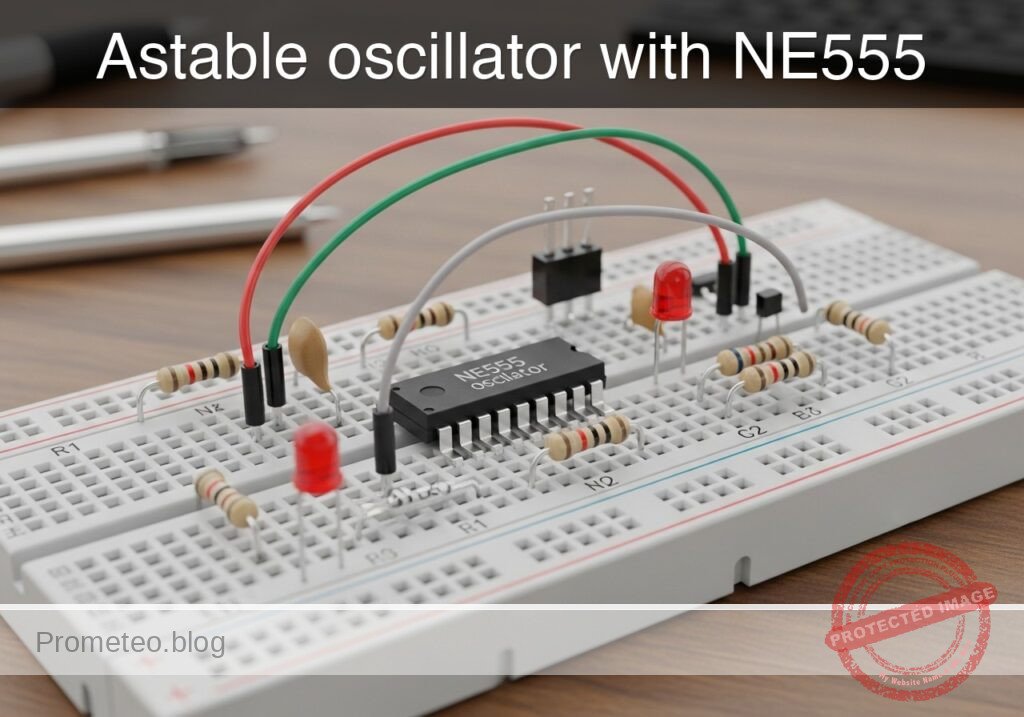
Practical case: astable oscillator with NE555

[ V1: 5 V DC ] --(+)--> [ VCC ]
[ V1: 5 V DC ] --(-)--> [ 0 ]

[ VCC ] --(pin8 supply)--> [ U1: NE555 astable core ] --(pin3 = VOUT)--> [ R3: 330 ohm ] --(LED_A)--> [ D1: Red LED ] --> [ 0 ]
[ VCC ] --(RESET to pin4)--> [ U1: NE555 astable core ]
[ VCC ] --(R1: 10 k ohm, RA)--> [ DIS / U1 pin7 ] --(R2: 68 k ohm, RB)--> [ TH_TR / U1 pins2+6 ] --(timing sense)--> [ U1: NE555 astable core ]
[ TH_TR / U1 pins2+6 ] --(C1: 10 uF, + to TH_TR, - to 0)--> [ 0 ]
[ U1 pin5 = CV ] --(C2: 10 nF noise filter to 0)--> [ 0 ]
[ VCC ] --(C3: 100 nF decoupling to 0, close to U1)--> [ 0 ]
[ U1 pin1 = GND ] --> [ 0 ]
Electrical diagram
Measurements and tests
- Power-off inspection
- Check that U1 pin 1 goes to 0 and U1 pin 8 goes to VCC.
- Verify that U1 pin 2 and U1 pin 6 are linked together at TH_TR.
-
Confirm LED polarity: anode toward R3, cathode toward 0.
-
Initial power test
- Apply 5 V from V1.
- The LED should start blinking immediately.
-
If the LED stays always on or always off, remove power and recheck wiring.
-
Measure output voltage
- Probe VOUT with a multimeter or oscilloscope.
- With an oscilloscope, expect a square-like waveform from near 0 V to near 5 V.
-
With a multimeter, the reading may show an average voltage between these limits, depending on blink speed.
-
Measure the timing node
- Probe TH_TR.
- Expect a repeating capacitor waveform rising from about 1.67 V to 3.33 V when VCC = 5 V.
-
This confirms the internal 1/3 VCC and 2/3 VCC thresholds of the NE555.
-
Check the control-voltage node
- Probe CV.
-
Expect a nearly steady voltage close to 2/3 VCC, around 3.3 V, with small ripple.
-
Estimate period and frequency
- Use the standard astable equations:
- T = 0.693 x (R1 + 2R2) x C1
- f = 1 / T
- With R1 = 10 kΩ, R2 = 68 kΩ, C1 = 10 µF:
- T ≈ 0.693 x (10k + 136k) x 10 µF ≈ 1.01 s
- f ≈ 0.99 Hz
-
Measured blinking should be close to 1 blink per second.
-
Estimate duty cycle
- Use:
- tHIGH = 0.693 x (R1 + R2) x C1
- tLOW = 0.693 x R2 x C1
- Duty cycle ≈ tHIGH / T
- For these values, duty cycle is about 53%.
- On the oscilloscope, the high time should be slightly longer than the low time.
SPICE netlist and simulation
Reference SPICE Netlist (ngspice) — excerptFull SPICE netlist (ngspice)
* Practical case: Astable oscillator with NE555
.width out=256

* Power Supply
V1 VCC 0 DC 5

* NE555 Timer IC Subcircuit Instance
* Pins: GND TRIG OUT RESET CTRL THRES DISCH VCC_PIN
XU1 0 TH_TR VOUT VCC CV TH_TR DISCH VCC NE555

* Timing Components
R1 VCC DISCH 10k
R2 DISCH TH_TR 47k
C1 TH_TR 0 10u
C2 CV 0 10n

* Output Load (LED)
R3 VOUT LED_A 330
D1 LED_A 0 DLED

* ... (truncated in public view) ...
Copy this content into a .cir file and run with ngspice.
* Practical case: Astable oscillator with NE555
.width out=256

* Power Supply
V1 VCC 0 DC 5

* NE555 Timer IC Subcircuit Instance
* Pins: GND TRIG OUT RESET CTRL THRES DISCH VCC_PIN
XU1 0 TH_TR VOUT VCC CV TH_TR DISCH VCC NE555

* Timing Components
R1 VCC DISCH 10k
R2 DISCH TH_TR 47k
C1 TH_TR 0 10u
C2 CV 0 10n

* Output Load (LED)
R3 VOUT LED_A 330
D1 LED_A 0 DLED

* Models
.MODEL DLED D(IS=1e-19 N=1.6 RS=10 BV=5 IBV=10u)

* Behavioral NE555 Subcircuit
.SUBCKT NE555 GND TRIG OUT RESET CTRL THRES DISCH VCC_PIN
* Internal voltage divider (3 x 5k resistors)
R1 VCC_PIN CTRL 5k
R2 CTRL N1 5k
R3 N1 GND 5k

* Smooth comparators for threshold, trigger, and reset
B_COMP_TH COMP_TH GND V=0.5*(1+tanh(100*(V(THRES,GND)-V(CTRL,GND))))
B_COMP_TR COMP_TR GND V=0.5*(1+tanh(100*(V(N1,GND)-V(TRIG,GND))))
B_COMP_RST COMP_RST GND V=0.5*(1+tanh(100*(0.7-V(RESET,GND))))

* SR Latch (Integrator with positive feedback for infinite hold time)
B_LATCH GND LATCH I=V(COMP_TR,GND) - V(COMP_TH,GND) - 5*V(COMP_RST,GND) + (V(LATCH,GND)>0.5 ? 0.1 : -0.1)
C_LATCH LATCH GND 1n
R_LATCH LATCH GND 100Meg

* Latch Voltage Clamps (Clamps V(LATCH) between ~0V and ~1V)
D1 GND LATCH D_CLAMP
V_CLAMP V_CLAMP_NODE GND 1
D2 LATCH V_CLAMP_NODE D_CLAMP
.model D_CLAMP D(N=0.01 RS=1)

* Output Driver Stage
B_OUT OUT_INT GND V=V(LATCH,GND)>0.5 ? V(VCC_PIN,GND) : 0.1
R_OUT OUT_INT OUT 10

* Open-Collector Discharge Transistor (Modeled as a Switch)
B_DISCH_CTRL DISCH_CTRL GND V=V(LATCH,GND)<0.5 ? 1 : 0
S_DISCH DISCH GND DISCH_CTRL GND SW_DISCH
.model SW_DISCH SW(VT=0.5 RON=15 ROFF=100Meg)
.ENDS

* Force initial condition on timing capacitor to ensure guaranteed oscillator startup
.ic V(TH_TR)=0

* Simulation Commands
.op
.tran 1m 3
.print tran V(VOUT) V(TH_TR) V(DISCH) V(LED_A) V(CV)
Simulation Results (Transient Analysis)

Show raw data table (3013 rows)
Index   time            v(vout)         v(th_tr)        v(disch)        v(led_a)        v(cv)
0	0.000000e+00	4.903386e+00	0.000000e+00	4.122467e+00	1.715117e+00	3.333333e+00
1	1.000000e-05	4.903386e+00	8.771053e-05	4.122482e+00	1.715117e+00	3.333333e+00
2	2.000000e-05	4.903386e+00	1.754195e-04	4.122498e+00	1.715117e+00	3.333333e+00
3	4.000000e-05	4.903386e+00	3.508344e-04	4.122529e+00	1.715117e+00	3.333333e+00
4	8.000000e-05	4.903386e+00	7.016457e-04	4.122590e+00	1.715117e+00	3.333333e+00
5	1.600000e-04	4.903386e+00	1.403195e-03	4.122713e+00	1.715117e+00	3.333333e+00
6	3.200000e-04	4.903386e+00	2.805997e-03	4.122959e+00	1.715117e+00	3.333333e+00
7	6.400000e-04	4.903386e+00	5.610420e-03	4.123451e+00	1.715117e+00	3.333333e+00
8	1.280000e-03	4.903386e+00	1.121455e-02	4.124434e+00	1.715117e+00	3.333333e+00
9	2.280000e-03	4.903386e+00	1.995841e-02	4.125968e+00	1.715117e+00	3.333333e+00
10	3.280000e-03	4.903386e+00	2.868694e-02	4.127499e+00	1.715117e+00	3.333333e+00
11	4.280000e-03	4.903386e+00	3.740018e-02	4.129028e+00	1.715117e+00	3.333333e+00
12	5.280000e-03	4.903386e+00	4.609814e-02	4.130554e+00	1.715117e+00	3.333333e+00
13	6.280000e-03	4.903386e+00	5.478085e-02	4.132077e+00	1.715117e+00	3.333333e+00
14	7.280000e-03	4.903386e+00	6.344835e-02	4.133597e+00	1.715117e+00	3.333333e+00
15	8.280000e-03	4.903386e+00	7.210065e-02	4.135115e+00	1.715117e+00	3.333333e+00
16	9.280000e-03	4.903386e+00	8.073778e-02	4.136630e+00	1.715117e+00	3.333333e+00
17	1.028000e-02	4.903386e+00	8.935978e-02	4.138143e+00	1.715117e+00	3.333333e+00
18	1.128000e-02	4.903386e+00	9.796666e-02	4.139653e+00	1.715117e+00	3.333333e+00
19	1.228000e-02	4.903386e+00	1.065585e-01	4.141160e+00	1.715117e+00	3.333333e+00
20	1.328000e-02	4.903386e+00	1.151352e-01	4.142665e+00	1.715117e+00	3.333333e+00
21	1.428000e-02	4.903386e+00	1.236969e-01	4.144166e+00	1.715117e+00	3.333333e+00
22	1.528000e-02	4.903386e+00	1.322436e-01	4.145666e+00	1.715117e+00	3.333333e+00
23	1.628000e-02	4.903386e+00	1.407753e-01	4.147162e+00	1.715117e+00	3.333333e+00
... (2989 more rows) ...
Reference SPICE netlist (ngspice)
* Practical case: Astable oscillator with NE555
.width out=256

* Power Supply
V1 VCC 0 DC 5

* NE555 Timer IC Subcircuit Instance
* Pins: GND TRIG OUT RESET CTRL THRES DISCH VCC_PIN
XU1 0 TH_TR VOUT VCC CV TH_TR DISCH VCC NE555

* Timing Components
R1 VCC DISCH 10k
R2 DISCH TH_TR 47k
C1 TH_TR 0 10u
C2 CV 0 10n

* Output Load (LED)
R3 VOUT LED_A 330
D1 LED_A 0 DLED

* Models
.MODEL DLED D(IS=1e-19 N=1.6 RS=10 BV=5 IBV=10u)

* Behavioral NE555 Subcircuit
.SUBCKT NE555 GND TRIG OUT RESET CTRL THRES DISCH VCC_PIN
* Internal voltage divider (3 x 5k resistors)
R1 VCC_PIN CTRL 5k
R2 CTRL N1 5k
R3 N1 GND 5k

* Smooth comparators for threshold, trigger, and reset
B_COMP_TH COMP_TH GND V=0.5*(1+tanh(100*(V(THRES,GND)-V(CTRL,GND))))
B_COMP_TR COMP_TR GND V=0.5*(1+tanh(100*(V(N1,GND)-V(TRIG,GND))))
B_COMP_RST COMP_RST GND V=0.5*(1+tanh(100*(0.7-V(RESET,GND))))

* SR Latch (Integrator with positive feedback for infinite hold time)
B_LATCH GND LATCH I=V(COMP_TR,GND) - V(COMP_TH,GND) - 5*V(COMP_RST,GND) + (V(LATCH,GND)>0.5 ? 0.1 : -0.1)
C_LATCH LATCH GND 1n
R_LATCH LATCH GND 100Meg

* Latch Voltage Clamps (Clamps V(LATCH) between ~0V and ~1V)
D1 GND LATCH D_CLAMP
V_CLAMP V_CLAMP_NODE GND 1
D2 LATCH V_CLAMP_NODE D_CLAMP
.model D_CLAMP D(N=0.01 RS=1)

* Output Driver Stage
B_OUT OUT_INT GND V=V(LATCH,GND)>0.5 ? V(VCC_PIN,GND) : 0.1
R_OUT OUT_INT OUT 10

* Open-Collector Discharge Transistor (Modeled as a Switch)
B_DISCH_CTRL DISCH_CTRL GND V=V(LATCH,GND)<0.5 ? 1 : 0
S_DISCH DISCH GND DISCH_CTRL GND SW_DISCH
.model SW_DISCH SW(VT=0.5 RON=15 ROFF=100Meg)
.ENDS

* Force initial condition on timing capacitor to ensure guaranteed oscillator startup
.ic V(TH_TR)=0

* Simulation Commands
.op
.tran 1m 3
.print tran V(VOUT) V(TH_TR) V(DISCH) V(LED_A) V(CV)
Simulation Results (Transient Analysis)
Common mistakes and how to avoid them
- Reversing the electrolytic capacitor
- Error: C1 installed with wrong polarity.
-
Fix: connect the positive terminal of C1 to TH_TR and the negative terminal to 0.
-
Wrong NE555 pin placement on the breadboard
- Error: pin numbering mirrored or shifted.
-
Fix: identify the notch or dot on the IC and count pins correctly before wiring.
-
Forgetting supply decoupling
- Error: omitting C3 causes unstable behavior or irregular blinking.
- Fix: place C3 = 100 nF directly between U1 pin 8 and U1 pin 1.
Troubleshooting
- Symptom: LED does not light at all
- Cause: no 5 V supply, wrong LED polarity, or open resistor path.
-
Fix: verify VCC, check D1 orientation, and confirm continuity from VOUT through R3 to D1.
-
Symptom: LED stays permanently on
- Cause: TH_TR not connected correctly, DIS wiring error, or R2 misplaced.
-
Fix: check that R2 is between DIS and TH_TR, and that pins 2 and 6 are tied together.
-
Symptom: LED stays permanently off
- Cause: RESET not tied high or output shorted.
-
Fix: connect U1 pin 4 directly to VCC and inspect VOUT for accidental grounding.
-
Symptom: Blink rate is much too fast or too slow
- Cause: wrong resistor value or wrong capacitor value.
-
Fix: measure R1, R2, and C1; replace parts with the intended values.
-
Symptom: Irregular or noisy waveform
- Cause: poor breadboard contacts or missing C2/C3.
- Fix: reseat the IC, shorten wiring, and install the bypass capacitors.
Possible improvements and extensions
- Add a frequency control
-
Replace R2 with a series combination of a fixed resistor and a potentiometer to adjust the blink rate.
-
Drive a buzzer or second indicator
- Use VOUT to control a transistor stage so the timer can flash a brighter LED or pulse a small buzzer.
More Practical Cases on Prometeo.blog
Find this product and/or books on this topic on Amazon
As an Amazon Associate, I earn from qualifying purchases. If you buy through this link, you help keep this project running.
Quick Quiz

Telecommunications Electronics Engineer and Computer Engineer (official degrees in Spain).