
Level: Basic. Build a circuit where a pilot light can be activated from two independent switches using digital logic.
Objective and use case
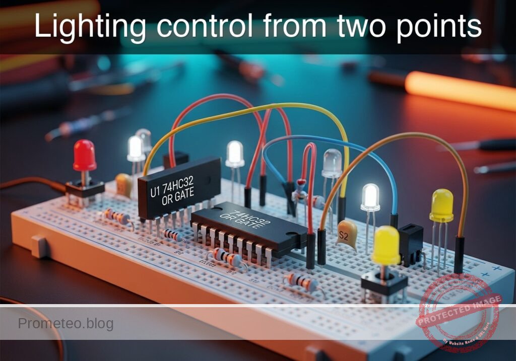
In this project, you will build a digital control circuit using a 74HC32 OR gate to power an LED indicator when either of two push buttons is actuated. This demonstrates the fundamental logic function where an output is true if at least one input is true.
Why it is useful:
* Home Automation: Simulates a hallway light system where multiple switches can turn on a light.
* Security Systems: Represents an alarm trigger zone where any single sensor (door or window) triggers the siren.
* Automotive: Functions like interior dome lights that turn on if the driver’s side OR passenger’s side door is opened.
* Industrial Safety: Acts as an emergency stop system where pressing any button on a production line halts the machine.
Expected outcome:
* LED State: The LED remains OFF (Logic 0) only when both buttons are released.
* Single Press: Pressing Button A turns the LED ON (Logic 1).
* Single Press: Pressing Button B turns the LED ON (Logic 1).
* Simultaneous Press: Pressing both buttons keeps the LED ON (Logic 1).
* Target Audience: Students and hobbyists learning basic digital logic gates.
Materials
- V1: 5 V DC supply
- U1: 74HC32 (Quad 2-Input OR Gate IC)
- S1: Momentary Push Button (NO – Normally Open), function: Input A
- S2: Momentary Push Button (NO – Normally Open), function: Input B
- R1: 10 kΩ resistor, function: Pull-down for Input A
- R2: 10 kΩ resistor, function: Pull-down for Input B
- R3: 330 Ω resistor, function: LED current limiting
- D1: Red LED, function: Logic output indicator
Pin-out of the IC used
Chip: 74HC32 (Quad 2-Input OR Gate)
| Pin | Name | Logic Function | Connection in this case |
|---|---|---|---|
| 1 | 1A | Input A | Connected to S1 and R1 |
| 2 | 1B | Input B | Connected to S2 and R2 |
| 3 | 1Y | Output | Connected to R3 (LED driver) |
| 7 | GND | Ground | Connected to 0V |
| 14 | VCC | Power Supply | Connected to +5V |
Wiring guide
This guide defines the connections using specific node names to ensure a clean circuit assembly.
-
Power Nodes:
VCC: Connect positive terminal of V1 to U1 Pin 14.0(GND): Connect negative terminal of V1 to U1 Pin 7.
-
Input A Logic (
NODE_A):- Connect S1 between
VCCandNODE_A. - Connect R1 between
NODE_Aand0(GND). - Connect U1 Pin 1 to
NODE_A.
- Connect S1 between
-
Input B Logic (
NODE_B):- Connect S2 between
VCCandNODE_B. - Connect R2 between
NODE_Band0(GND). - Connect U1 Pin 2 to
NODE_B.
- Connect S2 between
-
Output Logic (
NODE_Y):- Connect U1 Pin 3 to one end of R3.
- Connect the other end of R3 to the anode (long leg) of D1.
- Connect the cathode (short leg) of D1 to
0(GND).
Conceptual block diagram
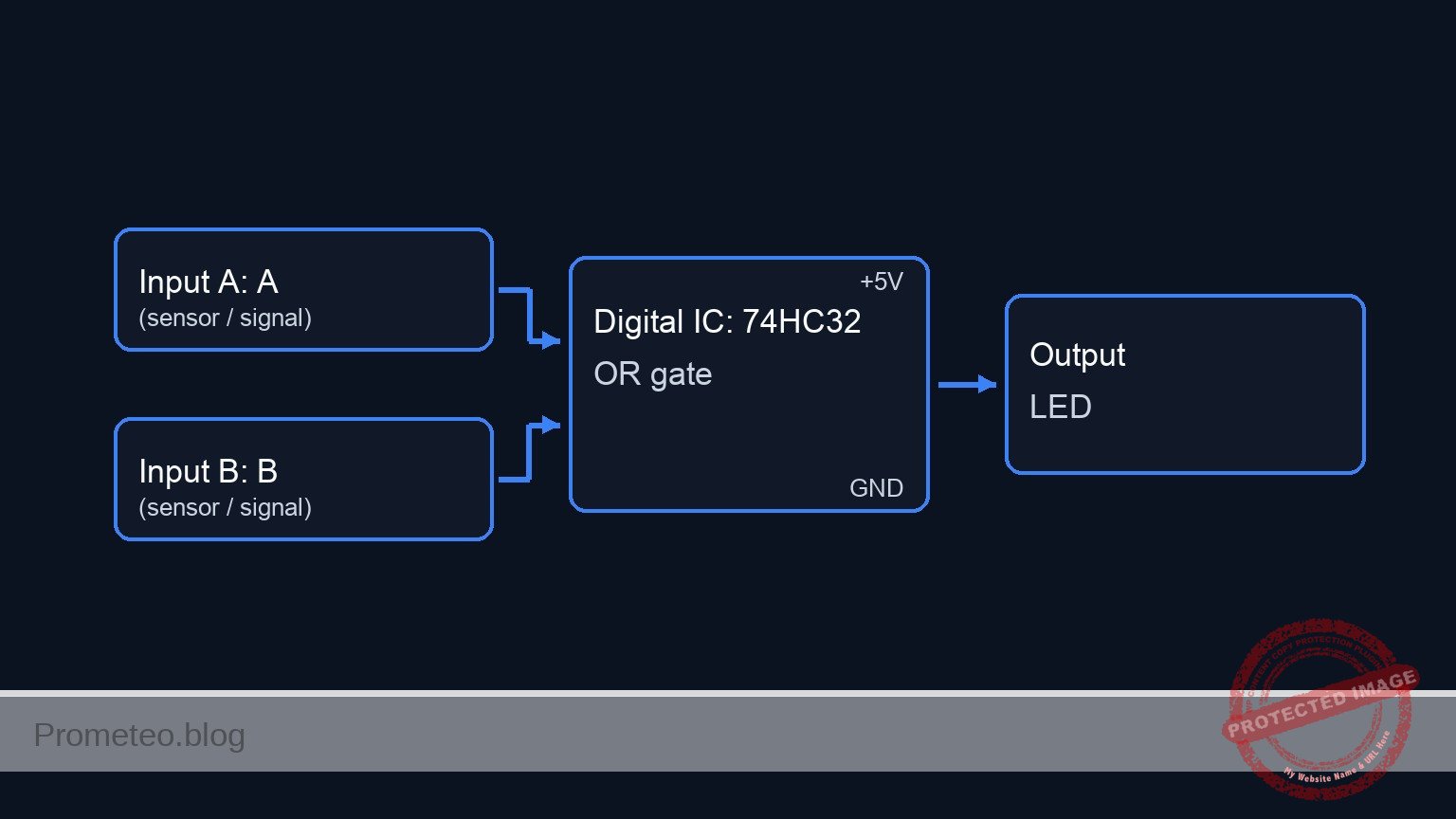
Schematic
[ INPUTS ]                                  [ LOGIC ]                                [ OUTPUT ]

[ VCC ]--> [ S1 (NO) ] --+--(NODE_A)----------->+-------------+
                         |  (Pin 1)             |             |
                    [ R1 (10k) ]                |  U1: 74HC32 |
                         v                      |  (OR Gate)  |--(NODE_Y)--> [ R3 (330) ] --> [ D1 (LED) ] --> [ GND ]
                      [ GND ]                   |  (Pin 3)    |
                                                |             |
[ VCC ]--> [ S2 (NO) ] --+--(NODE_B)----------->+-------------+
                         |  (Pin 2)
                    [ R2 (10k) ]
                         v
                      [ GND ]
Truth table
The 74HC32 follows the standard OR logic table:
| Input A (S1) | Input B (S2) | Output Y (LED) | State Description |
|---|---|---|---|
| 0 (Released) | 0 (Released) | 0 (OFF) | No active signal |
| 0 (Released) | 1 (Pressed) | 1 (ON) | Activated by B |
| 1 (Pressed) | 0 (Released) | 1 (ON) | Activated by A |
| 1 (Pressed) | 1 (Pressed) | 1 (ON) | Activated by both |
Measurements and tests
- Idle Check: Before pressing anything, measure the voltage at
NODE_AandNODE_Brelative to GND. It should be close to 0V (Logic 0) due to the pull-down resistors. The LED should be off. - Input A Test: Press S1. Measure voltage at
NODE_A; it should rise to 5V. Verify D1 lights up. - Input B Test: Press S2. Measure voltage at
NODE_B; it should rise to 5V. Verify D1 lights up. - Combined Test: Press both buttons simultaneously. The LED should remain lit without flickering.
SPICE netlist and simulation
Reference SPICE Netlist (ngspice) — excerptFull SPICE netlist (ngspice)
* Practical case: Lighting control from two points

* --- Power Supply ---
* V1: 5V DC Supply connected to VCC and GND (0)
V1 VCC 0 DC 5

* --- Input A ---
* S1: Momentary Push Button (NO)
* Modeled as a voltage-controlled switch (S1) driven by a pulse source (V_ACT_A)
* to simulate the physical user action of pressing the button.
V_ACT_A ACT_A 0 PULSE(0 5 50u 1u 1u 100u 200u)
S1 VCC NODE_A ACT_A 0 SW_BTN

* R1: 10k Pull-down resistor for Input A
R1 NODE_A 0 10k

* --- Input B ---
* S2: Momentary Push Button (NO)
* Modeled as a voltage-controlled switch (S2) driven by a pulse source (V_ACT_B)
V_ACT_B ACT_B 0 PULSE(0 5 50u 1u 1u 200u 400u)
S2 VCC NODE_B ACT_B 0 SW_BTN

* R2: 10k Pull-down resistor for Input B
R2 NODE_B 0 10k

* --- Logic IC U1: 74HC32 (Quad 2-Input OR Gate) ---
* Wiring Guide: Pin 1 to NODE_A, Pin 2 to NODE_B, Pin 3 to NODE_Y
* Pin 7 to GND (0), Pin 14 to VCC
XU1 NODE_A NODE_B NODE_Y 0 VCC 74HC32

* ... (truncated in public view) ...
Copy this content into a .cir file and run with ngspice.
* Practical case: Lighting control from two points

* --- Power Supply ---
* V1: 5V DC Supply connected to VCC and GND (0)
V1 VCC 0 DC 5

* --- Input A ---
* S1: Momentary Push Button (NO)
* Modeled as a voltage-controlled switch (S1) driven by a pulse source (V_ACT_A)
* to simulate the physical user action of pressing the button.
V_ACT_A ACT_A 0 PULSE(0 5 50u 1u 1u 100u 200u)
S1 VCC NODE_A ACT_A 0 SW_BTN

* R1: 10k Pull-down resistor for Input A
R1 NODE_A 0 10k

* --- Input B ---
* S2: Momentary Push Button (NO)
* Modeled as a voltage-controlled switch (S2) driven by a pulse source (V_ACT_B)
V_ACT_B ACT_B 0 PULSE(0 5 50u 1u 1u 200u 400u)
S2 VCC NODE_B ACT_B 0 SW_BTN

* R2: 10k Pull-down resistor for Input B
R2 NODE_B 0 10k

* --- Logic IC U1: 74HC32 (Quad 2-Input OR Gate) ---
* Wiring Guide: Pin 1 to NODE_A, Pin 2 to NODE_B, Pin 3 to NODE_Y
* Pin 7 to GND (0), Pin 14 to VCC
XU1 NODE_A NODE_B NODE_Y 0 VCC 74HC32

* --- Output Stage ---
* R3: 330 Ohm LED current limiting resistor
R3 NODE_Y NODE_LED 330

* D1: Red LED Logic output indicator
D1 NODE_LED 0 LED_RED

* --- Models and Subcircuits ---

* Switch Model (Normally Open)
* Vt=2.5V: Threshold voltage for switching
* Ron=0.1: Low resistance when closed
* Roff=10Meg: High resistance when open
.model SW_BTN SW(Vt=2.5 Ron=0.1 Roff=10Meg)

* LED Model (Generic Red LED)
.model LED_RED D(IS=1e-22 N=1.5 RS=5 BV=5 IBV=10u CJO=10p)

* 74HC32 Behavioral Subcircuit
* Implements robust continuous logic to avoid convergence issues
.subckt 74HC32 1 2 3 7 14
* Pin Definitions: 1=InputA, 2=InputB, 3=OutputY, 7=GND, 14=VCC
* Logic: Y = A OR B
* Implemented using Sigmoid function S(x) = 1 / (1 + exp(-k*(x-threshold)))
* OR(A,B) is equivalent to 1 - (NOT_A * NOT_B)
* V(14) scales the output to the supply rail
B_OR 3 7 V = V(14) * (1 - ( (1/(1+exp(-20*(V(1)-2.5)))) * (1/(1+exp(-20*(V(2)-2.5)))) ))
.ends

* --- Simulation Directives ---
* Transient analysis for 600us to capture all logic states of the pulses
.tran 1u 600u

* Print required voltages for analysis
.print tran V(NODE_A) V(NODE_B) V(NODE_Y) V(NODE_LED)

* Calculate DC operating point
.op

.end
Simulation Results (Transient Analysis)

Show raw data table (1562 rows)
Index   time            v(node_a)       v(node_b)       v(node_y)
0	0.000000e+00	4.995005e-03	4.995005e-03	5.000000e+00
1	1.000000e-08	4.995005e-03	4.995005e-03	5.000000e+00
2	2.000000e-08	4.995005e-03	4.995005e-03	5.000000e+00
3	4.000000e-08	4.995005e-03	4.995005e-03	5.000000e+00
4	8.000000e-08	4.995005e-03	4.995005e-03	5.000000e+00
5	1.600000e-07	4.995005e-03	4.995005e-03	5.000000e+00
6	3.200000e-07	4.995005e-03	4.995005e-03	5.000000e+00
7	6.400000e-07	4.995005e-03	4.995005e-03	5.000000e+00
8	1.280000e-06	4.995005e-03	4.995005e-03	5.000000e+00
9	2.280000e-06	4.995005e-03	4.995005e-03	5.000000e+00
10	3.280000e-06	4.995005e-03	4.995005e-03	5.000000e+00
11	4.280000e-06	4.995005e-03	4.995005e-03	5.000000e+00
12	5.280000e-06	4.995005e-03	4.995005e-03	5.000000e+00
13	6.280000e-06	4.995005e-03	4.995005e-03	5.000000e+00
14	7.280000e-06	4.995005e-03	4.995005e-03	5.000000e+00
15	8.280000e-06	4.995005e-03	4.995005e-03	5.000000e+00
16	9.280000e-06	4.995005e-03	4.995005e-03	5.000000e+00
17	1.028000e-05	4.995005e-03	4.995005e-03	5.000000e+00
18	1.128000e-05	4.995005e-03	4.995005e-03	5.000000e+00
19	1.228000e-05	4.995005e-03	4.995005e-03	5.000000e+00
20	1.328000e-05	4.995005e-03	4.995005e-03	5.000000e+00
21	1.428000e-05	4.995005e-03	4.995005e-03	5.000000e+00
22	1.528000e-05	4.995005e-03	4.995005e-03	5.000000e+00
23	1.628000e-05	4.995005e-03	4.995005e-03	5.000000e+00
... (1538 more rows) ...
Common mistakes and how to avoid them
- Leaving Inputs Floating: Failing to install pull-down resistors (R1, R2) causes the inputs to «float,» often leading to the LED flickering or staying on permanently due to static noise. Always tie unused inputs to GND or VCC.
- Missing Power to Chip: Forgetting to connect Pin 14 to +5V and Pin 7 to GND. The logic gates inside the chip cannot function without power.
- LED Orientation: Inserting the LED backwards (anode to ground). The LED will act as an open circuit and will never turn on.
Troubleshooting
- LED is always ON:
- Check if R1 or R2 is missing or disconnected.
- Verify you are using a Normally Open (NO) button, not a Normally Closed (NC) one.
- LED does not turn ON when buttons are pressed:
- Check U1 power connections (Pins 7 and 14).
- Ensure the LED is oriented correctly (Flat side/short leg to GND).
- LED is very dim:
- R3 value might be too high (e.g., using 10 kΩ instead of 330 Ω).
- Supply voltage V1 might be too low.
Possible improvements and extensions
- Three-Point Control: Cascade a second OR gate (using the remaining gates on the 74HC32 chip) to add a third switch, allowing control from three locations.
- Latch Circuit: Add a feedback loop or use an SR latch so that pressing a button once turns the light on and keeps it on until a «Reset» button is pressed (simulating an alarm memory).
More Practical Cases on Prometeo.blog
Find this product and/or books on this topic on Amazon
As an Amazon Associate, I earn from qualifying purchases. If you buy through this link, you help keep this project running.
Quick Quiz

Telecommunications Electronics Engineer and Computer Engineer (official degrees in Spain).

