
Level: Basic – Analyze speed and linearity differences between an LDR and a photodiode.
Objective and use case
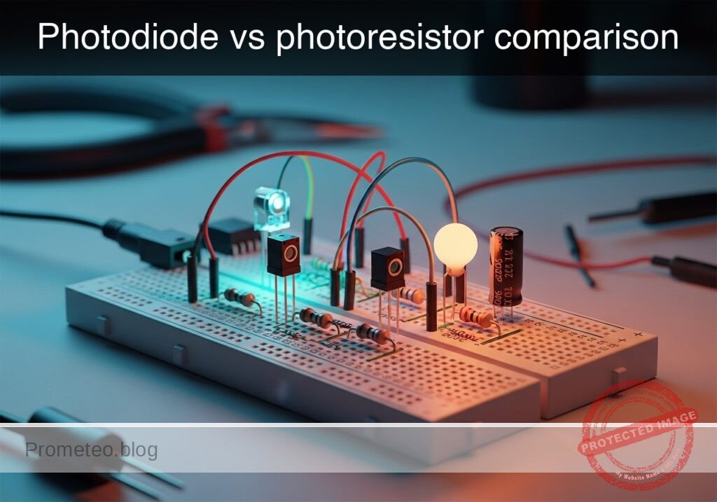
You will build a dual comparison circuit featuring a Light Dependent Resistor (LDR) and a Photodiode side-by-side, both stimulated by a pulsed LED light source. This setup demonstrates why specific sensors are chosen for different applications based on response time and linearity.
- High-speed data transmission: Photodiodes are essential for fiber optics and remote controls where signals switch rapidly.
- Ambient light sensing: LDRs are cost-effective for streetlights (dusk-to-dawn) where reaction speed does not matter.
- Precision metering: Photodiodes provide a linear current output proportional to light intensity, ideal for lux meters.
Expected outcome:
* LDR Output: A slow, curved voltage response («shark fin» shape) when exposed to a fast-blinking light.
* Photodiode Output: A sharp, square voltage response tracking the light source accurately.
* Voltage Levels: Distinct voltage changes at nodes V_LDR and V_PD corresponding to light intensity.
* Target Audience: Students and hobbyists interested in analog sensors and optoelectronics.
Materials
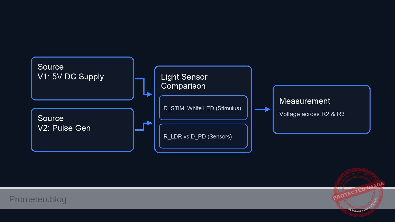
- V1: 5 V DC supply, function: Main circuit power.
- V2: 0 V to 5 V Pulse Generator (100 Hz), function: Driver for the test LED (Stimulus).
- R1: 330 Ω resistor, function: Current limiting for the stimulus LED.
- D_STIM: Green LED, function: Light source to trigger sensors (Chosen for distinct forward voltage).
- R_LDR: Light Dependent Resistor (LDR), function: Slow photo-resistive sensor.
- R2: 10 kΩ resistor, function: Voltage divider bottom leg for LDR.
- D_PD: Silicon Photodiode (e.g., BPW34), function: Fast photo-current sensor.
- R3: 220 kΩ resistor, function: Load resistor to convert photo-current to voltage.
Wiring guide
The circuit consists of three distinct sections: the Stimulus (pulsing light), the LDR divider, and the Photodiode divider.
Stimulus Section:
* V2 (Pulse Source) connects between V_PULSE and 0 (GND).
* R1 connects between V_PULSE and NODE_LED.
* D_STIM (Anode) connects to NODE_LED.
* D_STIM (Cathode) connects to 0 (GND).
* Note: Place D_STIM physically close to both R_LDR and D_PD to ensure they receive the light.
LDR Sensor Section:
* V1 (DC Source) connects between VCC and 0 (GND).
* R_LDR connects between VCC and V_LDR.
* R2 connects between V_LDR and 0 (GND).
Photodiode Sensor Section:
* D_PD (Cathode) connects to VCC. (Note: Photodiodes operate in reverse bias for photoconductive mode).
* D_PD (Anode) connects to V_PD.
* R3 connects between V_PD and 0 (GND).
Conceptual block diagram
Schematic
Title: Practical case: Photodiode vs photoresistor comparison

      [ INPUT SOURCES ]               [ SENSOR / OPTICAL BLOCK ]             [ OUTPUTS ]

                                   +--> [ R_LDR: Photoresistor ] --+------> < V_LDR >
                                   |    (Light Dependent Res.)     |
                                   |             ^                 v
                                   |             ~            [ R2: 10k ]
                                   |             ~ Light           |
    ( V1: 5 V DC Supply ) ----------+             ~                GND
                                   |             ~
                                   |             ~
                                   +--> [ D_PD: Photodiode ] ------+------> < V_PD >
                                        (Reverse Biased)           |
                                                 ^                 v
                                                 ~            [ R3: 220k ]
                                                 ~ Light           |
                                                 ~                GND
                                                 ~
                                                 ~
    ( V2: Pulse Gen ) --> [ R1: 330 ] --> [ D_STIM: Green LED ] ----------> GND
Measurements and tests
To validate the differences between the sensors, follow these steps:
-
Static Testing (DC):
- Turn off V2 (Pulse). Keep V1 (5 V) on.
- Cover both sensors (Dark condition). Measure voltage at
V_LDRandV_PD. Both should be close to 0 V. - Shine a constant light (using the Green LED or a flashlight). Measure voltage at
V_LDRandV_PD. Both voltages should rise significantly.
-
Dynamic Testing (AC/Response Time):
- Enable V2 (Pulse Generator) at 100 Hz (50% duty cycle).
- Connect Oscilloscope Channel 1 to
V_PULSE(Reference). - Connect Oscilloscope Channel 2 to
V_LDR. - Connect Oscilloscope Channel 3 to
V_PD. - Observation: Compare the waveforms. Channel 3 (Photodiode) should look like a square wave, matching Channel 1. Channel 2 (LDR) will look distorted, with slow rising and falling edges («shark fin»), failing to reach full amplitude if the frequency is too high.
SPICE netlist and simulation
Reference SPICE Netlist (ngspice) — excerptFull SPICE netlist (ngspice)
* Practical case: Photodiode vs photoresistor comparison

* --- Component Models ---
* Generic Green LED Model
.model DLED D(IS=1e-22 RS=5 N=1.5 CJO=10p)
* Silicon Photodiode Model (BPW34 - Dark Characteristics)
.model D_BPW34 D(IS=1e-9 RS=5 N=1 CJO=20p)

* --- Power Supplies ---
* V1: Main Circuit Power (5V DC)
V1 VCC 0 DC 5

* V2: Pulse Generator (Stimulus)
* 0V to 5V, 100Hz (10ms period), 50% Duty Cycle
* Rise/Fall time 100us to ensure convergence
V2 V_PULSE 0 PULSE(0 5 0 100u 100u 5m 10m)

* --- Stimulus Section ---
* R1: Current limiting resistor for LED
R1 V_PULSE NODE_LED 330
* ... (truncated in public view) ...
Copy this content into a .cir file and run with ngspice.
* Practical case: Photodiode vs photoresistor comparison

* --- Component Models ---
* Generic Green LED Model
.model DLED D(IS=1e-22 RS=5 N=1.5 CJO=10p)
* Silicon Photodiode Model (BPW34 - Dark Characteristics)
.model D_BPW34 D(IS=1e-9 RS=5 N=1 CJO=20p)

* --- Power Supplies ---
* V1: Main Circuit Power (5V DC)
V1 VCC 0 DC 5

* V2: Pulse Generator (Stimulus)
* 0V to 5V, 100Hz (10ms period), 50% Duty Cycle
* Rise/Fall time 100us to ensure convergence
V2 V_PULSE 0 PULSE(0 5 0 100u 100u 5m 10m)

* --- Stimulus Section ---
* R1: Current limiting resistor for LED
R1 V_PULSE NODE_LED 330

* D_STIM: Green LED (Light Source)
* Anode to NODE_LED, Cathode to GND
D_STIM NODE_LED 0 DLED

* --- Light Coupling & Physics Simulation (Behavioral) ---
* These elements simulate the physical behavior of light transfer
* from the LED to the sensors.

* 1. LDR Latency Simulation (RC Filter)
* Simulates the slow response time of the photo-resistive material.
* R_PHYS and C_PHYS create a delay on the control signal.
R_PHYS NODE_LED V_LIGHT_LDR 10k
C_PHYS V_LIGHT_LDR 0 1u

* --- LDR Sensor Section ---
* R_LDR: Light Dependent Resistor
* Modeled as a behavioral resistor (ngspice syntax).
* Resistance varies from ~1Meg (Dark) to ~2k (Light).
* Controlled by the delayed light signal (V_LIGHT_LDR) with a sigmoid transition.
R_LDR VCC V_LDR R = '2k + (1Meg - 2k) / (1 + exp(10 * (V(V_LIGHT_LDR) - 1.0)))'

* R2: Voltage divider bottom leg (10k)
R2 V_LDR 0 10k

* --- Photodiode Sensor Section ---
* D_PD: Silicon Photodiode (BPW34)
* Connected in reverse bias: Cathode to VCC, Anode to V_PD.
D_PD V_PD VCC D_BPW34

* Photocurrent Source (Behavioral)
* Represents the current generated by light (Cathode to Anode).
* Controlled directly by NODE_LED (Fast response).
* Generates ~20uA when LED is ON.
B_PD_PHOTO VCC V_PD I = '20u * (1 / (1 + exp(-10 * (V(NODE_LED) - 1.0))))'

* R3: Load resistor for Photodiode (220k)
* Converts photocurrent to voltage.
R3 V_PD 0 220k

* --- Simulation Directives ---
.op
* Transient analysis: 100us step size, 30ms duration (3 full cycles)
.tran 100u 30m

* Print directives for logging results
.print tran V(V_PULSE) V(NODE_LED) V(V_LDR) V(V_PD)

.end
Simulation Results (Transient Analysis)

Show raw data table (764 rows)
Index   time            v(v_pulse)      v(node_led)     v(v_ldr)
0	0.000000e+00	0.000000e+00	2.716431e-145	4.950717e-02
1	1.000000e-06	5.000000e-02	4.824684e-02	4.950717e-02
2	1.083830e-06	5.419150e-02	5.230192e-02	4.950717e-02
3	1.251490e-06	6.257451e-02	6.041598e-02	4.950717e-02
4	1.586811e-06	7.934053e-02	7.664554e-02	4.950717e-02
5	2.257451e-06	1.128726e-01	1.091032e-01	4.950717e-02
6	3.598733e-06	1.799366e-01	1.740197e-01	4.950717e-02
7	6.281296e-06	3.140648e-01	3.038499e-01	4.950717e-02
8	1.164642e-05	5.823211e-01	5.635005e-01	4.950718e-02
9	2.048297e-05	1.024149e+00	9.911337e-01	4.950719e-02
10	3.049268e-05	1.524634e+00	1.474550e+00	4.950722e-02
11	3.675621e-05	1.837811e+00	1.660693e+00	4.950724e-02
12	4.338068e-05	2.169034e+00	1.711124e+00	4.950727e-02
13	4.777134e-05	2.388567e+00	1.729852e+00	4.950729e-02
14	5.403581e-05	2.701791e+00	1.750179e+00	4.950731e-02
15	6.656476e-05	3.328238e+00	1.778506e+00	4.950737e-02
16	9.162266e-05	4.581133e+00	1.819947e+00	4.950748e-02
17	1.000000e-04	5.000000e+00	1.831535e+00	4.950751e-02
18	1.050116e-04	5.000000e+00	1.831601e+00	4.950754e-02
19	1.150347e-04	5.000000e+00	1.831470e+00	4.950759e-02
20	1.350811e-04	5.000000e+00	1.831473e+00	4.950768e-02
21	1.751737e-04	5.000000e+00	1.831478e+00	4.950788e-02
22	2.553590e-04	5.000000e+00	1.831491e+00	4.950831e-02
23	3.553590e-04	5.000000e+00	1.831507e+00	4.950895e-02
... (740 more rows) ...
Common mistakes and how to avoid them
- Reversing the Photodiode: A photodiode in a divider setup usually requires reverse bias (Cathode to VCC). If connected forward (Anode to VCC), it acts like a normal diode, clamping the voltage and ruining the sensing range.
- Using too small a resistor for the Photodiode: Photodiodes generate very small currents (microamps). Using a 1 kΩ resistor for R3 will result in tiny signals. We use 220 kΩ here to ensure the output voltage swing is large enough to see clearly on an oscilloscope.
- Expecting the LDR to react instantly: Students often think the circuit is broken because the LDR signal looks «rounded» or «wavy» at high frequencies. This is the inherent physical limitation of the chemical material (Cadmium Sulfide), not a wiring error.
Troubleshooting
- Symptom: No voltage change on
V_PDwhen light shines.- Cause: Photodiode might be reversed or R3 is too small for the ambient light level.
- Fix: Ensure Cathode is at VCC and Anode is at the measurement node. Check that the Stimulus LED is actually blinking and bright enough.
- Symptom:
V_LDRis always stuck at High (near 5 V).- Cause: R_LDR resistance is too low compared to R2, or ambient light is too bright.
- Fix: Ensure the «dark» test is actually dark. Decrease R2 if the LDR resistance is naturally low.
- Symptom:
V_PDsignal is extremely noisy.- Cause: High impedance node (
V_PDwith 220 kΩ resistor) picks up mains hum (50/60Hz). - Fix: Use shorter wires or add a small capacitor (e.g., 100pF) in parallel with R3, though this slightly reduces speed.
- Cause: High impedance node (
Possible improvements and extensions
- Transimpedance Amplifier (TIA): Replace the passive resistor R3 with an Op-Amp configured as a transimpedance amplifier. This provides a much faster response and a low-impedance output suitable for driving other circuits.
- Frequency Sweep: Use a variable frequency generator for V2. Slowly increase the frequency from 10 Hz to 10 kHz to find the «cutoff frequency» where the LDR stops responding completely, while the photodiode continues to work.
More Practical Cases on Prometeo.blog
Quick Quiz

Telecommunications Electronics Engineer and Computer Engineer (official degrees in Spain).

