
Level: Advanced. Design a redundant safety system enabling catalyst injection only when three critical variables are within range.
Objective and use case
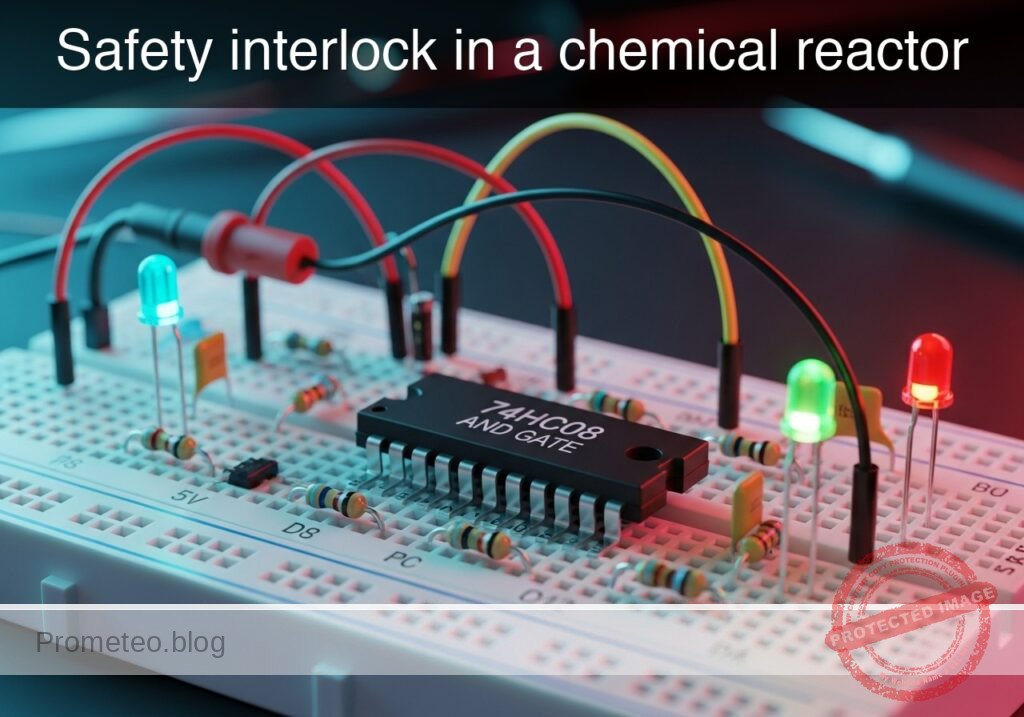
In this case, you will build a hardware-based safety interlock logic circuit that monitors three simulated analog parameters (Temperature, Pressure, Level). It uses comparators to digitize these signals and a cascaded logic gate arrangement to control a high-power relay.
Why it is useful:
* Industrial Safety: Prevents chemical reactions from starting unless environmental conditions are perfect, avoiding run-away thermal events.
* Machine Guarding: Ensures guards are closed, pressure is released, and motors are stopped before unlocking maintenance doors.
* Medical Devices: Prevents laser or radiation emission unless all interlocks (key switch, door contact, patient sensor) are active.
Expected outcome:
* Logic Output: The final control signal V_SAFE goes HIGH (Logic 1, ~5V) only when all three inputs are within the «Safe» zone simultaneously.
* Visual Indication: The Relay activates (closing the circuit for the catalyst valve) and a Green LED lights up only in the 1-1-1 state.
* Hysteresis: The system maintains stability near switching thresholds (dependent on comparator configuration).
Target audience: Electronics engineering students and industrial automation technicians.
Materials
- V1: 5 V DC power supply, function: Logic and sensor power.
- U1: 74HC08, function: Quad 2-input AND gate (used to create 3-input logic).
- U2: LM339, function: Quad open-collector comparator (digitizes analog sensors).
- R1: 10 kΩ potentiometer, function: Simulator for Temperature Sensor.
- R2: 10 kΩ potentiometer, function: Simulator for Pressure Sensor.
- R3: 10 kΩ potentiometer, function: Simulator for Tank Level.
- R_REF: 10 kΩ resistor array (or pots), function: Voltage dividers for reference thresholds (2.5 V).
- R_PU1: 4.7 kΩ resistor, function: Pull-up for Comparator 1 output.
- R_PU2: 4.7 kΩ resistor, function: Pull-up for Comparator 2 output.
- R_PU3: 4.7 kΩ resistor, function: Pull-up for Comparator 3 output.
- R_BASE: 1 kΩ resistor, function: Transistor base current limiting.
- Q1: 2N2222 NPN Transistor, function: Relay driver.
- K1: 5 V Relay, function: Actuator for catalyst valve.
- D1: 1N4007 Diode, function: Flyback protection for Q1.
- D2: Green LED, function: Indicator for «Injection Active».
- R_LED: 330 Ω resistor, function: LED current limiting.
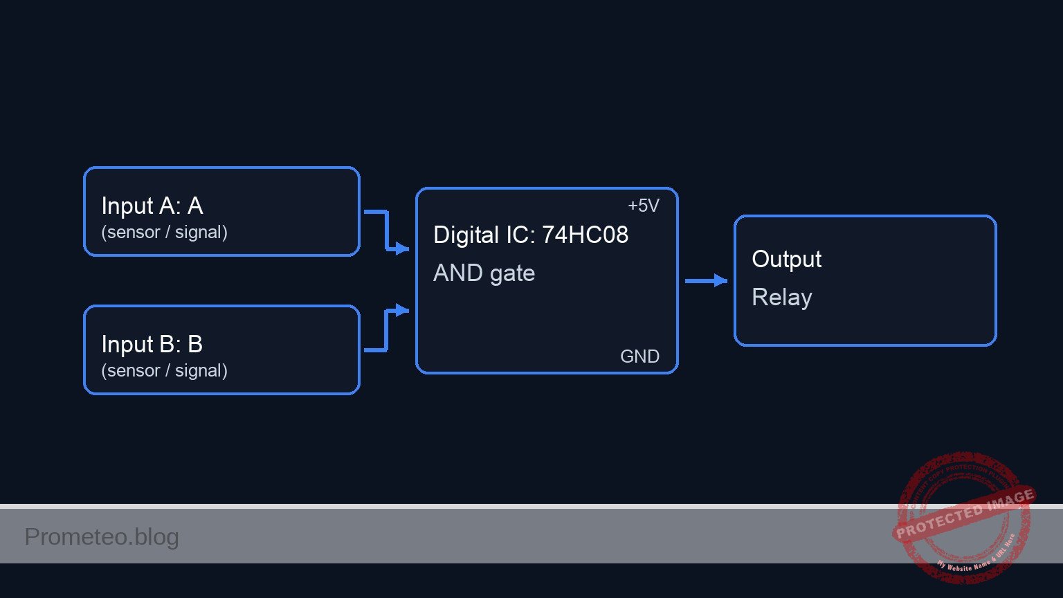
Pin-out of the IC used
Selected Chip: 74HC08 (Quad 2-Input AND Gate)
| Pin | Name | Logic function | Connection in this case |
|---|---|---|---|
| 1 | 1A | Input A (Gate 1) | Connected to Temperature Status (SIG_TEMP) |
| 2 | 1B | Input B (Gate 1) | Connected to Pressure Status (SIG_PRES) |
| 3 | 1Y | Output (Gate 1) | Intermediate result (Temp AND Pres) |
| 4 | 2A | Input A (Gate 2) | Connected to 1Y (Intermediate result) |
| 5 | 2B | Input B (Gate 2) | Connected to Level Status (SIG_LEV) |
| 6 | 2Y | Output (Gate 2) | Final Safety Signal (V_SAFE) |
| 7 | GND | Ground | Connected to power supply 0 |
| 14 | VCC | Power | Connected to VCC (+5V) |
Wiring guide
Power Supply
* V1 connects between VCC and 0 (GND).
* U1 (74HC08) Pin 14 connects to VCC, Pin 7 to 0.
* U2 (LM339) Pin 3 (V+) connects to VCC, Pin 12 (GND) to 0.
Analog Inputs & Comparators (Signal Conditioning)
* R1 (Temp Pot) connects between VCC and 0; wiper connects to U2 Input 1- (NODE_T_SENS).
* Reference divider connects to U2 Input 1+ (NODE_REF).
* U2 Output 1 connects to SIG_TEMP.
* R_PU1 connects between VCC and SIG_TEMP (required for open-collector).
* R2 (Pres Pot) connects between VCC and 0; wiper connects to U2 Input 2- (NODE_P_SENS).
* Reference divider connects to U2 Input 2+ (NODE_REF).
* U2 Output 2 connects to SIG_PRES.
* R_PU2 connects between VCC and SIG_PRES.
* R3 (Level Pot) connects between VCC and 0; wiper connects to U2 Input 3- (NODE_L_SENS).
* Reference divider connects to U2 Input 3+ (NODE_REF).
* U2 Output 13 connects to SIG_LEV.
* R_PU3 connects between VCC and SIG_LEV.
Digital Logic (Cascading for 3-Input AND)
* U1 Pin 1 (1A) connects to SIG_TEMP.
* U1 Pin 2 (1B) connects to SIG_PRES.
* U1 Pin 3 (1Y) connects to U1 Pin 4 (2A).
* U1 Pin 5 (2B) connects to SIG_LEV.
* U1 Pin 6 (2Y) connects to V_SAFE.
Output Stage
* R_BASE connects between V_SAFE and NODE_BASE.
* Q1 Base connects to NODE_BASE.
* Q1 Emitter connects to 0.
* Q1 Collector connects to NODE_RELAY.
* K1 (Relay coil) connects between VCC and NODE_RELAY.
* D1 connects between NODE_RELAY (Anode) and VCC (Cathode) Note: Check polarity, cathode to positive for flyback.
* R_LED connects between NODE_RELAY and NODE_LED_A.
* D2 connects between NODE_LED_A and 0.
Conceptual block diagram
Schematic
Title: Practical case: Safety interlock in a chemical reactor

      [ SENSORS / INPUTS ]           [ SIGNAL CONDITIONING ]               [ LOGIC PROCESSING ]                  [ OUTPUT ACTUATOR STAGE ]

                                         (VCC / Pull-ups)                                                         (VCC 5V Source)
                                                |                                                                        |
    [ R1: Temp Pot ] --(Analog)--> [ U2: LM339 Comp 1 ] --(SIG_TEMP)-->+                                    +------------+------------+
    (Simulates Sensor)             [ Ref: 2.5V Divider]                |                                    |            |            |
                                                                       v                                [ K1 Relay ] [ D1 Diode ] [ R_LED ]
                                                                [ U1: 74HC08 ]                          [  Coil    ] [ Cathode^ ] [   +     ]
    [ R2: Pres Pot ] --(Analog)--> [ U2: LM339 Comp 2 ] --(SIG_PRES)-->[  AND Gate A  ] --(Intermed)--> |            [ Anode v  ] [ D2 LED  ]
    (Simulates Sensor)             [ Ref: 2.5V Divider]                [              ]       |         |            |            |
                                                                                              |         +------------+------------+
                                                                                              v                      |
                                                                                        [ U1: 74HC08 ]               | (NODE_RELAY)
                                                                                        [  AND Gate B  ]             v
    [ R3: Levl Pot ] --(Analog)--> [ U2: LM339 Comp 3 ] --(SIG_LEV)--->(Pin 5)--------->[              ] --(V_SAFE)--> [ R_BASE ] --> [ Q1: 2N2222 ]
    (Simulates Sensor)             [ Ref: 2.5V Divider]                                 [              ]                              [ NPN Base   ]
                                                                                                                                      [            ]
                                                                                                                                      [ Collector  ] --< (Sinks Current)
                                                                                                                                      [ Emitter    ]
                                                                                                                                             |
                                                                                                                                            GND
Truth table
This table represents the cascaded logic (Temp AND Pressure AND Level).
| Temp OK (A) | Pres OK (B) | Level OK (C) | Intermediate (A·B) | Final Output (V_SAFE) | Action |
|---|---|---|---|---|---|
| 0 | 0 | 0 | 0 | 0 | Safe Mode (Off) |
| 0 | 0 | 1 | 0 | 0 | Safe Mode (Off) |
| 0 | 1 | 0 | 0 | 0 | Safe Mode (Off) |
| 0 | 1 | 1 | 0 | 0 | Safe Mode (Off) |
| 1 | 0 | 0 | 0 | 0 | Safe Mode (Off) |
| 1 | 0 | 1 | 0 | 0 | Safe Mode (Off) |
| 1 | 1 | 0 | 1 | 0 | Safe Mode (Off) |
| 1 | 1 | 1 | 1 | 1 | Inject Catalyst |
Measurements and tests
- Individual Sensor Test: Adjust R1 (Temp) below the threshold. Verify
SIG_TEMPgoes HIGH (approx 5V). Repeat for R2 and R3. - Logic Logic Validation: Set Temp and Pressure to «Safe» (High logic), but Level to «Unsafe» (Low logic). Measure U1 Pin 3 (Intermediate); it should be HIGH. Measure U1 Pin 6 (
V_SAFE); it should be LOW. - Full Activation: Set all three potentiometers to the «Safe» range. Verify
V_SAFEis HIGH, Q1 saturates, and the Relay (K1) clicks «On». - Response Time: Connect an oscilloscope channel 1 to
SIG_LEVand channel 2 toV_SAFE. Toggle the Level switch and measure the propagation delay (typically nanoseconds for the gate, milliseconds for the relay).
SPICE netlist and simulation
Reference SPICE Netlist (ngspice) — excerptFull SPICE netlist (ngspice)
* Practical case: Safety interlock in a chemical reactor

* --- Models ---
* Generic NPN Transistor
.model 2N2222MOD NPN(IS=1E-14 VAF=100 BF=200 IKF=0.3 XTB=1.5 BR=3 CJC=8E-12 CJE=25E-12 TR=46.91E-9 TF=411.1E-12 ITF=0.6 VTF=1.7 XTF=3 RB=10 RC=1 RE=0.1)
* Flyback Diode
.model D1N4007 D(IS=7.02767n RS=0.03415 N=1.2686 EG=1.11 XTI=3 BV=1000 IBV=10m CJO=10p VJ=0.7 M=0.5 FC=0.5 TT=100n)
* Green LED Indicator
.model LED_GREEN D(IS=1e-22 RS=5 N=1.5 CJO=50p BV=5 IBV=10u EG=2.1)
* Voltage Controlled Switch for Open Collector Comparator
* Vt=0: Switch state changes when control voltage crosses 0V
* Ron=10: Low resistance when closed (Logic 0 / Low)
* Roff=100Meg: High resistance when open (Logic 1 / High via Pull-up)
.model SW_OC SW(Vt=0 Vh=0.001 Ron=10 Roff=100Meg)

* --- Power Supply ---
* V1: 5 V DC power supply
V1 VCC 0 DC 5

* --- Reference Voltage (R_REF) ---
* Function: Voltage dividers for reference thresholds (2.5 V)
* Wiring: Reference divider connects to U2 Input + (NODE_REF)
R_REF_A VCC NODE_REF 10k
R_REF_B NODE_REF 0 10k

* --- Sensors (Simulated with PWL Voltage Sources) ---
* R1, R2, R3 Potentiometers simulated by PWL sources at the wiper nodes.
* Logic: Low Voltage (<2.5V) = Safe. High Voltage (>2.5V) = Unsafe/Alarm.
* Sequence: T=Safe, then Temp Fault, then Pres Fault, then Level Fault.

* ... (truncated in public view) ...
Copy this content into a .cir file and run with ngspice.
* Practical case: Safety interlock in a chemical reactor

* --- Models ---
* Generic NPN Transistor
.model 2N2222MOD NPN(IS=1E-14 VAF=100 BF=200 IKF=0.3 XTB=1.5 BR=3 CJC=8E-12 CJE=25E-12 TR=46.91E-9 TF=411.1E-12 ITF=0.6 VTF=1.7 XTF=3 RB=10 RC=1 RE=0.1)
* Flyback Diode
.model D1N4007 D(IS=7.02767n RS=0.03415 N=1.2686 EG=1.11 XTI=3 BV=1000 IBV=10m CJO=10p VJ=0.7 M=0.5 FC=0.5 TT=100n)
* Green LED Indicator
.model LED_GREEN D(IS=1e-22 RS=5 N=1.5 CJO=50p BV=5 IBV=10u EG=2.1)
* Voltage Controlled Switch for Open Collector Comparator
* Vt=0: Switch state changes when control voltage crosses 0V
* Ron=10: Low resistance when closed (Logic 0 / Low)
* Roff=100Meg: High resistance when open (Logic 1 / High via Pull-up)
.model SW_OC SW(Vt=0 Vh=0.001 Ron=10 Roff=100Meg)

* --- Power Supply ---
* V1: 5 V DC power supply
V1 VCC 0 DC 5

* --- Reference Voltage (R_REF) ---
* Function: Voltage dividers for reference thresholds (2.5 V)
* Wiring: Reference divider connects to U2 Input + (NODE_REF)
R_REF_A VCC NODE_REF 10k
R_REF_B NODE_REF 0 10k

* --- Sensors (Simulated with PWL Voltage Sources) ---
* R1, R2, R3 Potentiometers simulated by PWL sources at the wiper nodes.
* Logic: Low Voltage (<2.5V) = Safe. High Voltage (>2.5V) = Unsafe/Alarm.
* Sequence: T=Safe, then Temp Fault, then Pres Fault, then Level Fault.

* R1: Temp Sensor Simulator
V_SENS_T NODE_T_SENS 0 PWL(0 1 100u 1 101u 4 200u 4 201u 1)

* R2: Pressure Sensor Simulator
V_SENS_P NODE_P_SENS 0 PWL(0 1 300u 1 301u 4 400u 4 401u 1)

* R3: Tank Level Simulator
V_SENS_L NODE_L_SENS 0 PWL(0 1 500u 1 501u 4 600u 4 601u 1)

* --- U2: LM339 Quad Comparator ---
* Function: Digitizes analog sensors. Open Collector Outputs.
* Logic: If V(In-) > V(In+), Switch closes to Ground (Output Low).
*        Else Switch opens (Output High via Pull-up).

* Comparator 1 (Temperature)
* Wiring: Wiper (NODE_T_SENS) to Input 1-, Ref to Input 1+, Output to SIG_TEMP
S_COMP1 SIG_TEMP 0 NODE_T_SENS NODE_REF SW_OC
* R_PU1: Pull-up for Comparator 1
R_PU1 VCC SIG_TEMP 4.7k

* Comparator 2 (Pressure)
* Wiring: Wiper (NODE_P_SENS) to Input 2-, Ref to Input 2+, Output to SIG_PRES
S_COMP2 SIG_PRES 0 NODE_P_SENS NODE_REF SW_OC
* R_PU2: Pull-up for Comparator 2
R_PU2 VCC SIG_PRES 4.7k

* Comparator 3 (Level)
* Wiring: Wiper (NODE_L_SENS) to Input 3-, Ref to Input 3+, Output to SIG_LEV
S_COMP3 SIG_LEV 0 NODE_L_SENS NODE_REF SW_OC
* R_PU3: Pull-up for Comparator 3
R_PU3 VCC SIG_LEV 4.7k

* --- U1: 74HC08 Quad 2-input AND ---
* Function: Safety Logic.
* Modeled using Behavioral Sources (Sigmoid function for HC logic levels).

* Gate 1 (Pins 1, 2, 3)
* Inputs: SIG_TEMP, SIG_PRES. Output: NODE_AND_INT
B_AND1 NODE_AND_INT 0 V = 5 * (1 / (1 + exp(-20*(V(SIG_TEMP)-2.5)))) * (1 / (1 + exp(-20*(V(SIG_PRES)-2.5))))

* Gate 2 (Pins 4, 5, 6)
* Inputs: NODE_AND_INT (Pin 4 connects to Pin 3), SIG_LEV. Output: V_SAFE
B_AND2 V_SAFE 0 V = 5 * (1 / (1 + exp(-20*(V(NODE_AND_INT)-2.5)))) * (1 / (1 + exp(-20*(V(SIG_LEV)-2.5))))

* --- Output Stage ---

* R_BASE: Transistor base current limiting
R_BASE V_SAFE NODE_BASE 1k

* Q1: 2N2222 NPN Transistor, Relay driver
* Wiring: Base to NODE_BASE, Emitter to 0, Collector to NODE_RELAY
Q1 NODE_RELAY NODE_BASE 0 2N2222MOD

* K1: 5 V Relay Coil
* Wiring: Connects between VCC and NODE_RELAY
* Modeled as Inductor and Series Resistor
L_K1 VCC NODE_RELAY_INT 10m
R_K1 NODE_RELAY_INT NODE_RELAY 100

* D1: Flyback protection
* Wiring: Anode to NODE_RELAY, Cathode to VCC
D1 NODE_RELAY VCC D1N4007

* D2 & R_LED: Indicator "Injection Active"
* Corrected Wiring: LED should be parallel to Relay Coil to indicate Activation.
* Path: VCC -> Resistor -> LED Anode -> LED Cathode -> Collector (NODE_RELAY).
* When Q1 is ON (Relay Active), NODE_RELAY is Low (~0.2V), LED turns ON.
R_LED VCC NODE_LED_A 330
D2 NODE_LED_A NODE_RELAY LED_GREEN

* --- Analysis Directives ---
* Transient analysis to observe the sequence of sensor faults
.tran 1u 800u

* Print required signals
.print tran V(NODE_T_SENS) V(NODE_P_SENS) V(NODE_L_SENS)
.print tran V(SIG_TEMP) V(SIG_PRES) V(SIG_LEV)
.print tran V(NODE_AND_INT) V(V_SAFE)
.print tran V(NODE_RELAY) V(NODE_BASE)

.end
Simulation Results (Transient Analysis)

Show raw data table (3828 rows)
Index   time            v(node_t_sens)  v(node_p_sens)  v(node_l_sens)
0	0.000000e+00	1.000000e+00	1.000000e+00	1.000000e+00
1	1.000000e-08	1.000000e+00	1.000000e+00	1.000000e+00
2	2.000000e-08	1.000000e+00	1.000000e+00	1.000000e+00
3	4.000000e-08	1.000000e+00	1.000000e+00	1.000000e+00
4	8.000000e-08	1.000000e+00	1.000000e+00	1.000000e+00
5	1.600000e-07	1.000000e+00	1.000000e+00	1.000000e+00
6	3.200000e-07	1.000000e+00	1.000000e+00	1.000000e+00
7	6.400000e-07	1.000000e+00	1.000000e+00	1.000000e+00
8	1.280000e-06	1.000000e+00	1.000000e+00	1.000000e+00
9	2.280000e-06	1.000000e+00	1.000000e+00	1.000000e+00
10	3.280000e-06	1.000000e+00	1.000000e+00	1.000000e+00
11	4.280000e-06	1.000000e+00	1.000000e+00	1.000000e+00
12	5.280000e-06	1.000000e+00	1.000000e+00	1.000000e+00
13	6.280000e-06	1.000000e+00	1.000000e+00	1.000000e+00
14	7.280000e-06	1.000000e+00	1.000000e+00	1.000000e+00
15	8.280000e-06	1.000000e+00	1.000000e+00	1.000000e+00
16	9.280000e-06	1.000000e+00	1.000000e+00	1.000000e+00
17	1.028000e-05	1.000000e+00	1.000000e+00	1.000000e+00
18	1.128000e-05	1.000000e+00	1.000000e+00	1.000000e+00
19	1.228000e-05	1.000000e+00	1.000000e+00	1.000000e+00
20	1.328000e-05	1.000000e+00	1.000000e+00	1.000000e+00
21	1.428000e-05	1.000000e+00	1.000000e+00	1.000000e+00
22	1.528000e-05	1.000000e+00	1.000000e+00	1.000000e+00
23	1.628000e-05	1.000000e+00	1.000000e+00	1.000000e+00
... (3804 more rows) ...
Common mistakes and how to avoid them
- Missing Pull-up Resistors: The LM339 comparator has an open-collector output. If you forget R_PU1/2/3, the logic gate inputs will float or remain LOW. Always tie outputs to VCC via a resistor (e.g., 4.7kΩ).
- Floating Unused Inputs: The 74HC08 is a CMOS device. If pins 9, 10, 12, 13 (Gates 3 and 4) are left floating, they pick up noise and increase power consumption. Connect unused inputs to GND.
- Inductive Kickback: Omitting D1 (Flyback diode) across the relay coil. This will generate a high voltage spike when the relay turns off, destroying transistor Q1 immediately.
Troubleshooting
- Relay chatters (buzzing sound): The analog inputs are hovering exactly at the threshold voltage. Fix: Add a feedback resistor (hysteresis) between the comparator output and the non-inverting input.
- Logic output is always HIGH: Check the comparator inputs. If the reference voltage is reversed (e.g., Ref > Signal vs Signal > Ref), the logic might be inverted.
- Transistor gets hot but relay doesn’t switch: Q1 might be receiving insufficient base current, or the pinout (E-B-C) is incorrect. Fix: Verify R_BASE value and transistor pinout.
Possible improvements and extensions
- Latch Circuit: Add a feedback loop (or a Set-Reset latch) so that if safety is breached, the system shuts down and requires a manual «Reset» button press to restart, even if conditions return to normal.
- Fault Identification: Add red LEDs to the output of each comparator (inverted) to indicate exactly which variable (Temperature, Pressure, or Level) caused the shutdown.
More Practical Cases on Prometeo.blog
Find this product and/or books on this topic on Amazon
As an Amazon Associate, I earn from qualifying purchases. If you buy through this link, you help keep this project running.
Quick Quiz

Telecommunications Electronics Engineer and Computer Engineer (official degrees in Spain).

