
Level: Advanced — Design a circuit to approve a motion if at least one of three judges emits a positive vote, integrating combinational logic and signal debouncing.
Objective and use case
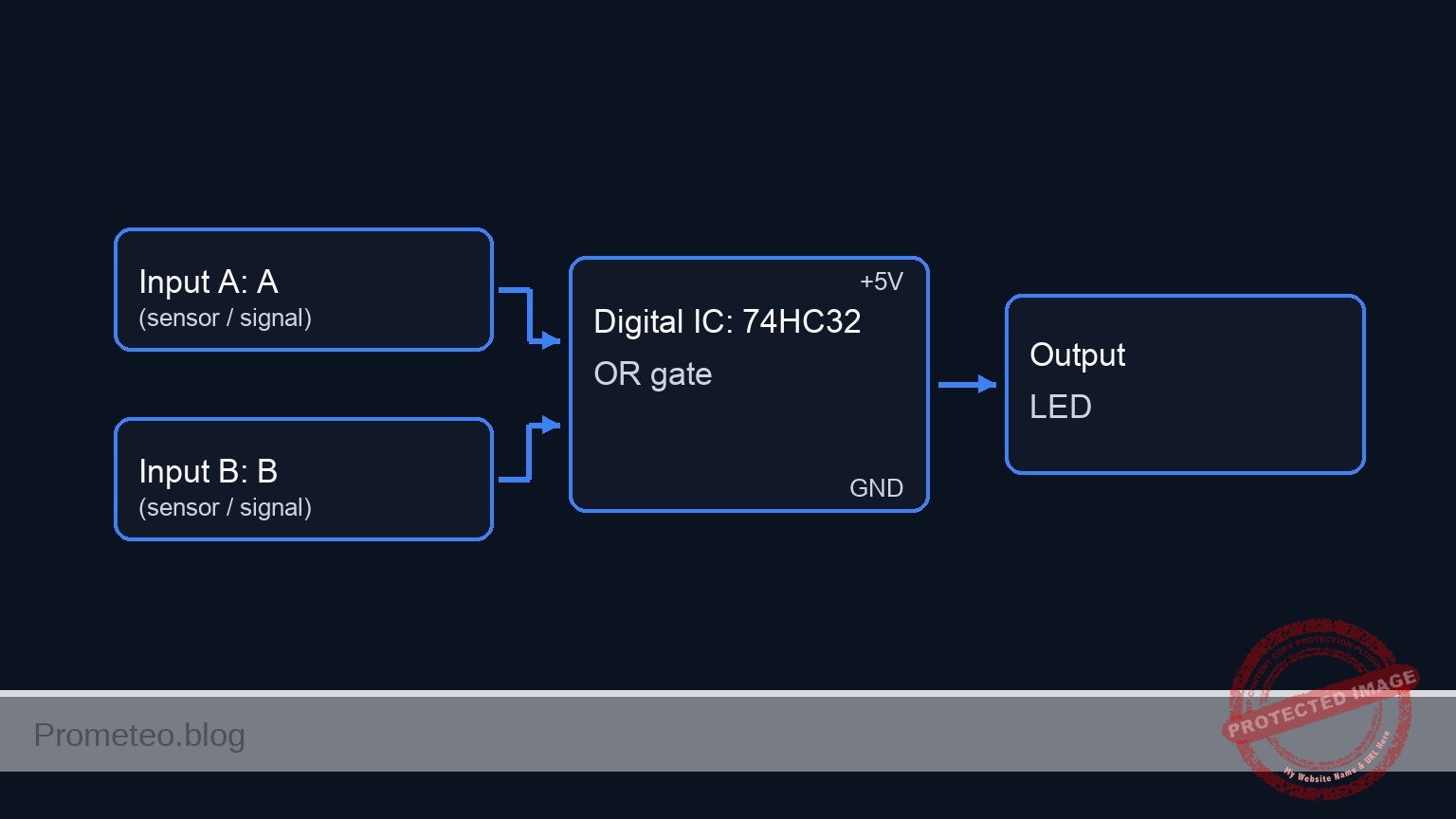
You will build a digital logic circuit that processes signals from three independent momentary switches representing judges. The system uses a cascaded OR topology to drive a visual indicator if any single input (or combination of inputs) is active.
Why it is useful:
* Safety Interlocks: Similar logic is used in machine guards where breaking any single beam or opening any door must trigger a stop or alarm.
* Fault Detection: In automotive dashboards, multiple sensors (oil, tire pressure, engine heat) feed into a central warning light (Check Engine) via OR logic.
* Access Control: Systems where multiple different credentials (card, code, or biometric) can grant entry to the same door.
* Interrupt Requests: In microcontrollers, multiple peripherals can trigger a single interrupt line to the CPU using this logic.
Expected outcome:
* The output LED turns ON (Logic High) if Judge A, Judge B, Judge C, or any combination presses their button.
* The output LED remains OFF (Logic Low) only when all buttons are released.
* Input signals are conditioned (debounced) to prevent rapid flickering caused by mechanical switch bounce.
* Verification of signal propagation through cascaded logic gates.
Target audience: Engineering students and advanced electronics enthusiasts.
Materials
- V1: 5 V DC supply
- S1: Momentary push-button (Normally Open), function: Judge A Input
- S2: Momentary push-button (Normally Open), function: Judge B Input
- S3: Momentary push-button (Normally Open), function: Judge C Input
- R1: 10 kΩ resistor, function: pull-down for Node A
- R2: 10 kΩ resistor, function: pull-down for Node B
- R3: 10 kΩ resistor, function: pull-down for Node C
- R4: 1 kΩ resistor, function: RC debounce series resistance (Input A)
- R5: 1 kΩ resistor, function: RC debounce series resistance (Input B)
- R6: 1 kΩ resistor, function: RC debounce series resistance (Input C)
- C1: 100 nF capacitor, function: debounce filtering (Input A)
- C2: 100 nF capacitor, function: debounce filtering (Input B)
- C3: 100 nF capacitor, function: debounce filtering (Input C)
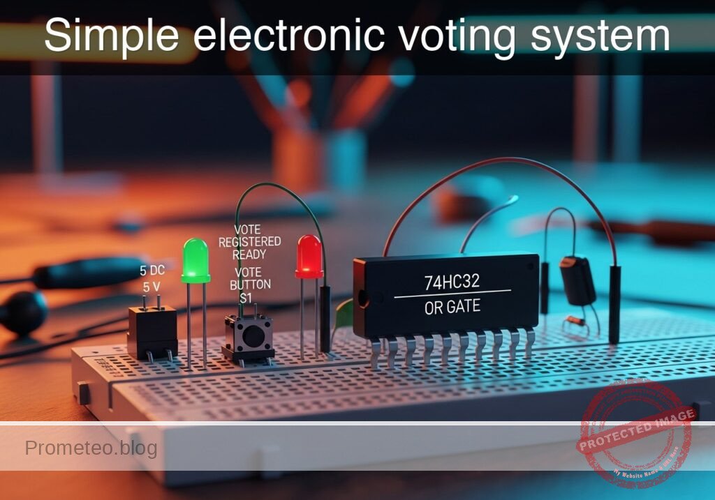
- U1: 74HC32 (Quad 2-Input OR Gate IC)
- R7: 330 Ω resistor, function: LED current limiting
- D1: Red LED, function: Outcome indicator
Pin-out of the IC used
Chip Selected: 74HC32 (Quad 2-Input OR Gate).
Note: Since we have 3 inputs and the chip contains 2-input gates, we will cascade two gates to create the logic function $Y = (A + B) + C$.
| Pin | Name | Logic function | Connection in this case |
|---|---|---|---|
| 1 | 1A | Input | Connects to Debounced Signal A |
| 2 | 1B | Input | Connects to Debounced Signal B |
| 3 | 1Y | Output | Connects to Pin 4 (Cascade to next gate) |
| 4 | 2A | Input | Connects to Pin 3 (Result of A+B) |
| 5 | 2B | Input | Connects to Debounced Signal C |
| 6 | 2Y | Output | Connects to Output LED circuit |
| 7 | GND | Ground | Connects to 0 (GND) |
| 14 | VCC | Power | Connects to VCC (+5V) |
Wiring guide
This guide uses SPICE-friendly node names.
* Power Supply:
* V1 connects between node VCC and node 0 (GND).
* U1 pin 14 connects to VCC.
* U1 pin 7 connects to 0.
- Input Stage (Judge A) – Pull-down & Debounce:
- S1 connects between
VCCand nodeRAW_A. - R1 connects between
RAW_Aand0. - R4 connects between
RAW_Aand nodeIN_A. -
C1 connects between
IN_Aand0. -
Input Stage (Judge B) – Pull-down & Debounce:
- S2 connects between
VCCand nodeRAW_B. - R2 connects between
RAW_Band0. - R5 connects between
RAW_Band nodeIN_B. -
C2 connects between
IN_Band0. -
Input Stage (Judge C) – Pull-down & Debounce:
- S3 connects between
VCCand nodeRAW_C. - R3 connects between
RAW_Cand0. - R6 connects between
RAW_Cand nodeIN_C. -
C3 connects between
IN_Cand0. -
Logic Processing (Cascaded OR):
- U1 pin 1 connects to
IN_A. - U1 pin 2 connects to
IN_B. - U1 pin 3 (Gate 1 Output) connects to node
GATE1_OUT. - U1 pin 4 connects to node
GATE1_OUT(Cascading signal). - U1 pin 5 connects to
IN_C. -
U1 pin 6 (Final Output) connects to node
LOGIC_OUT. -
Output Stage:
- R7 connects between
LOGIC_OUTand nodeLED_ANODE. - D1 connects between
LED_ANODE(Anode) and0(Cathode).
Conceptual block diagram
Schematic
[ INPUT / CONDITIONING ]                  [ LOGIC PROCESSING (74HC32) ]             [ OUTPUT ]

                                                +-------------------------+
    [ S1: Judge A ]                             |        U1: Gate 1       |
    (VCC -> RAW_A) -> [ R1/R4/C1 ] --(Pin 1)--->| Input A                 |
                      (Debounce)                |           OR            |
                                                | Input B       (Output)  |
    [ S2: Judge B ]                    +------->| Pin 2          Pin 3    |--+
    (VCC -> RAW_B) -> [ R2/R5/C2 ] ----+        +-------------------------+  |
                      (Debounce)                                             |
                                                                             |
                                                                             |
                                                +-------------------------+  |
                                                |        U1: Gate 2       |  |
                                                | (Cascade In)   Pin 4    |< +
                                                |           OR            |
    [ S3: Judge C ]                    +------->| Input C        (Output) |
    (VCC -> RAW_C) -> [ R3/R6/C3 ] ----+        | Pin 5          Pin 6    |-----> [ R7: 330 Ohm ]
                      (Debounce)                +-------------------------+           |
                                                                                      v
                                                                                 [ D1: Red LED ]
                                                                                      |
                                                                                      v
                                                                                     GND
Truth table
The system creates a 3-Input OR function: $Q = A + B + C$.
| Input A | Input B | Input C | Output Q (LED) | Note |
|---|---|---|---|---|
| 0 | 0 | 0 | 0 | Motion Rejected |
| 0 | 0 | 1 | 1 | Motion Approved |
| 0 | 1 | 0 | 1 | Motion Approved |
| 0 | 1 | 1 | 1 | Motion Approved |
| 1 | 0 | 0 | 1 | Motion Approved |
| 1 | 0 | 1 | 1 | Motion Approved |
| 1 | 1 | 0 | 1 | Motion Approved |
| 1 | 1 | 1 | 1 | Motion Approved |
Measurements and tests
- Static Logic Check: Ensure no buttons are pressed. Measure voltage at U1 Pin 6. It should be close to 0 V. Press S1. The voltage should rise to ~5 V. Repeat for S2 and S3 individually.
- Debounce Validation: Connect an oscilloscope to
RAW_AandIN_A. Press S1.RAW_Amay show sharp voltage spikes/noise on contact.IN_Ashould show a smooth exponential rise curve, filtering out the noise before it hits the logic gate. - Cascaded Delay: This is an advanced measurement. Measure the propagation delay between
IN_AandLOGIC_OUTversusIN_CandLOGIC_OUT. BecauseIN_Amust pass through two gates (Gate 1 then Gate 2), the total propagation delay will be slightly longer thanIN_C, which only passes through Gate 2.
SPICE netlist and simulation
Reference SPICE Netlist (ngspice) — excerptFull SPICE netlist (ngspice)
* Simple electronic voting system
* Based on Practical Case BOM and Wiring Guide

* --- Power Supply ---
* V1 connects between node VCC and node 0 (GND).
V1 VCC 0 DC 5

* --- User Input Stimuli (Button Presses) ---
* We simulate the physical push-buttons using Voltage Controlled Switches (S1-S3)
* controlled by independent PULSE sources (V_CTRL_A, etc.) to mimic user behavior.
* The timing is staggered to test inputs A, B, and C sequentially with sufficient
* time for the RC debounce circuits to charge and discharge.

* Judge A: Press at 1ms, hold for 2ms (releases at 3ms)
V_CTRL_A CTRL_A 0 PULSE(0 5 1m 1u 1u 2m 20m)

* Judge B: Press at 6ms, hold for 2ms (releases at 8ms)
V_CTRL_B CTRL_B 0 PULSE(0 5 6m 1u 1u 2m 20m)

* Judge C: Press at 11ms, hold for 2ms (releases at 13ms)
* ... (truncated in public view) ...
Copy this content into a .cir file and run with ngspice.
* Simple electronic voting system
* Based on Practical Case BOM and Wiring Guide

* --- Power Supply ---
* V1 connects between node VCC and node 0 (GND).
V1 VCC 0 DC 5

* --- User Input Stimuli (Button Presses) ---
* We simulate the physical push-buttons using Voltage Controlled Switches (S1-S3)
* controlled by independent PULSE sources (V_CTRL_A, etc.) to mimic user behavior.
* The timing is staggered to test inputs A, B, and C sequentially with sufficient
* time for the RC debounce circuits to charge and discharge.

* Judge A: Press at 1ms, hold for 2ms (releases at 3ms)
V_CTRL_A CTRL_A 0 PULSE(0 5 1m 1u 1u 2m 20m)

* Judge B: Press at 6ms, hold for 2ms (releases at 8ms)
V_CTRL_B CTRL_B 0 PULSE(0 5 6m 1u 1u 2m 20m)

* Judge C: Press at 11ms, hold for 2ms (releases at 13ms)
V_CTRL_C CTRL_C 0 PULSE(0 5 11m 1u 1u 2m 20m)

* --- Input Stage: Judge A ---
* S1 connects between VCC and node RAW_A
S1 VCC RAW_A CTRL_A 0 SW_PB
* R1 (10k) pull-down for Node A (RAW_A to 0)
R1 RAW_A 0 10k
* R4 (1k) RC debounce series resistance (RAW_A to IN_A)
R4 RAW_A IN_A 1k
* C1 (100nF) debounce filtering (IN_A to 0)
C1 IN_A 0 100n

* --- Input Stage: Judge B ---
* S2 connects between VCC and node RAW_B
S2 VCC RAW_B CTRL_B 0 SW_PB
* R2 (10k) pull-down for Node B (RAW_B to 0)
R2 RAW_B 0 10k
* R5 (1k) RC debounce series resistance (RAW_B to IN_B)
R5 RAW_B IN_B 1k
* C2 (100nF) debounce filtering (IN_B to 0)
C2 IN_B 0 100n

* --- Input Stage: Judge C ---
* S3 connects between VCC and node RAW_C
S3 VCC RAW_C CTRL_C 0 SW_PB
* R3 (10k) pull-down for Node C (RAW_C to 0)
R3 RAW_C 0 10k
* R6 (1k) RC debounce series resistance (RAW_C to IN_C)
R6 RAW_C IN_C 1k
* C3 (100nF) debounce filtering (IN_C to 0)
C3 IN_C 0 100n

* --- Logic Processing: U1 (74HC32 Quad 2-Input OR Gate) ---
* Implemented using Behavioral Voltage Sources (B-sources) for robust simulation.
* Logic Transfer Function: Continuous Sigmoid approximation of OR gate.
* Vout = VCC * Sigmoid( max(Input1, Input2) - Threshold )
* Threshold set to 2.5V (Mid-rail).
* U1 Pin 14 (VCC) and Pin 7 (GND) are functionally represented by the V(VCC) term and node 0 reference.

* Gate 1: Inputs IN_A (Pin 1), IN_B (Pin 2) -> Output GATE1_OUT (Pin 3)
* Corresponds to wiring: U1 pin 1 to IN_A, U1 pin 2 to IN_B, U1 pin 3 to GATE1_OUT
B_U1_G1 GATE1_OUT 0 V = V(VCC) * (1 / (1 + exp(-20 * (max(V(IN_A), V(IN_B)) - 2.5))))

* Cascading Connection:
* Wiring: U1 pin 4 connects to node GATE1_OUT.

* Gate 2: Inputs GATE1_OUT (Pin 4), IN_C (Pin 5) -> Output LOGIC_OUT (Pin 6)
* Corresponds to wiring: U1 pin 4 to GATE1_OUT, U1 pin 5 to IN_C, U1 pin 6 to LOGIC_OUT
B_U1_G2 LOGIC_OUT 0 V = V(VCC) * (1 / (1 + exp(-20 * (max(V(GATE1_OUT), V(IN_C)) - 2.5))))

* --- Output Stage ---
* R7 connects between LOGIC_OUT and node LED_ANODE
R7 LOGIC_OUT LED_ANODE 330
* D1 connects between LED_ANODE (Anode) and 0 (Cathode)
D1 LED_ANODE 0 D_LED

* --- Models ---
* Switch model for push buttons (Active High control)
.model SW_PB SW(Vt=2.5 Ron=0.1 Roff=10Meg)
* Generic LED model (Red)
.model D_LED D(IS=1n N=2 RS=10 BV=5)

* --- Simulation Directives ---
* Transient analysis for 15ms to capture all button presses and RC discharge curves.
* Step size 10us is sufficient for the 100us/1.1ms time constants.
.tran 10u 15m

* Print required nodes for validation
.print tran V(IN_A) V(IN_B) V(IN_C) V(GATE1_OUT) V(LOGIC_OUT) V(LED_ANODE)

.op
.end
Simulation Results (Transient Analysis)

Show raw data table (3274 rows)
Index   time            v(in_a)         v(in_b)         v(in_c)
0	0.000000e+00	4.995005e-03	4.995005e-03	4.995005e-03
1	1.000000e-07	4.995005e-03	4.995005e-03	4.995005e-03
2	2.000000e-07	4.995005e-03	4.995005e-03	4.995005e-03
3	4.000000e-07	4.995005e-03	4.995005e-03	4.995005e-03
4	8.000000e-07	4.995005e-03	4.995005e-03	4.995005e-03
5	1.600000e-06	4.995005e-03	4.995005e-03	4.995005e-03
6	3.200000e-06	4.995005e-03	4.995005e-03	4.995005e-03
7	6.400000e-06	4.995005e-03	4.995005e-03	4.995005e-03
8	1.280000e-05	4.995005e-03	4.995005e-03	4.995005e-03
9	2.280000e-05	4.995005e-03	4.995005e-03	4.995005e-03
10	3.280000e-05	4.995005e-03	4.995005e-03	4.995005e-03
11	4.280000e-05	4.995005e-03	4.995005e-03	4.995005e-03
12	5.280000e-05	4.995005e-03	4.995005e-03	4.995005e-03
13	6.280000e-05	4.995005e-03	4.995005e-03	4.995005e-03
14	7.280000e-05	4.995005e-03	4.995005e-03	4.995005e-03
15	8.280000e-05	4.995005e-03	4.995005e-03	4.995005e-03
16	9.280000e-05	4.995005e-03	4.995005e-03	4.995005e-03
17	1.028000e-04	4.995005e-03	4.995005e-03	4.995005e-03
18	1.128000e-04	4.995005e-03	4.995005e-03	4.995005e-03
19	1.228000e-04	4.995005e-03	4.995005e-03	4.995005e-03
20	1.328000e-04	4.995005e-03	4.995005e-03	4.995005e-03
21	1.428000e-04	4.995005e-03	4.995005e-03	4.995005e-03
22	1.528000e-04	4.995005e-03	4.995005e-03	4.995005e-03
23	1.628000e-04	4.995005e-03	4.995005e-03	4.995005e-03
... (3250 more rows) ...
Common mistakes and how to avoid them
- Floating Inputs: Failing to install the pull-down resistors (R1, R2, R3). Without them, the 74HC32 inputs act as antennas, causing the LED to flicker randomly or stay stuck High. Solution: Always reference inputs to GND when the switch is open.
- Ignoring Pinout: Connecting Input C to Pin 3 (which is an output). This creates a short circuit when the gate tries to drive Low while the button drives High. Solution: Double-check the datasheet pin diagram before powering up.
- Excessive RC Time Constant: Using a capacitor that is too large (e.g., 100 µF) for the debounce circuit. This creates a very slow voltage rise that causes the digital gate to oscillate linearly during the threshold crossing. Solution: Stick to 100 nF – 1 µF for simple logic inputs.
Troubleshooting
- LED is always ON: Check pull-down resistors. If measured voltage at pins 1, 2, or 5 is floating (not 0 V), the gate interprets it as Logic High.
- LED does not light up for Judge A or B: Verify the cascade connection. Pin 3 (Output of first gate) must be physically wired to Pin 4 (Input of second gate).
- Erratic behavior when touching wires: Indicates missing ground connections on unused inputs (if any) or floating operational inputs. Ensure all grounds share a common point.
- Gate gets hot: Check for output-to-output short circuits or output-to-VCC shorts. Disconnect power immediately.
Possible improvements and extensions
- Majority Vote Extension: Modify the logic to require at least two positive votes to approve the motion (using a combination of AND and OR gates: $AB + BC + AC$).
- Latch functionality: Add a D Flip-Flop (e.g., 74HC74) after the output. Once the motion is approved (LED ON), the light stays ON until a dedicated «Reset» button is pressed by a supervisor.
More Practical Cases on Prometeo.blog
        <div class="amazon-affiliate">
          <p><strong>Find this product and/or books on this topic on Amazon</strong></p>
          <p><a class="amazon-affiliate-btn" href="https://amzn.to/4mt8r4C" target="_blank" rel="nofollow sponsored noopener">Go to Amazon</a></p>
          <p class="amazon-affiliate-disclaimer">As an Amazon Associate, I earn from qualifying purchases. If you buy through this link, you help keep this project running.</p>
        </div>
Quick Quiz

Telecommunications Electronics Engineer and Computer Engineer (official degrees in Spain).

