

Level: Basic – Observe how an inductor filters high frequencies in an RL series circuit.
Objective and use case
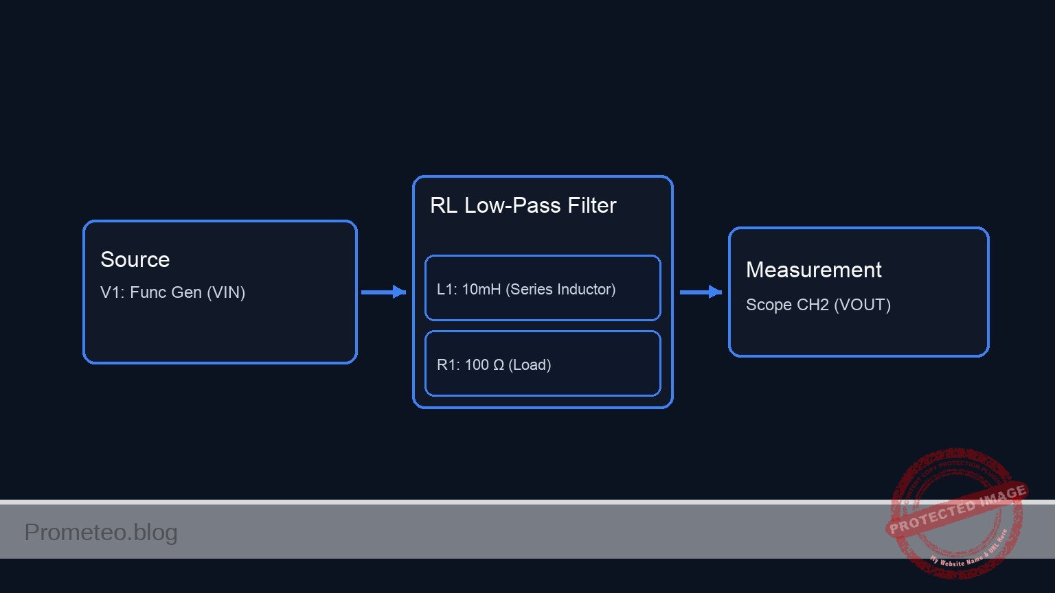
In this practical exercise, you will build a passive RL low-pass filter using a series inductor and a shunt resistor. This circuit demonstrates the inductive reactance property, where impedance increases with frequency, effectively blocking high-frequency signals while allowing low-frequency signals to pass through to the output.
Why it is useful:
* Audio Electronics: Used in crossover networks to direct low frequencies (bass) to woofers while blocking treble.
* Power Supplies: Essential for smoothing output currents and reducing ripple in DC/DC converters.
* Noise Suppression: Filters out high-frequency interference (EMI) on signal lines.
* Signal Conditioning: Removes high-frequency noise from sensor data before processing.
Expected outcome:
* Low Frequency Input (< Cutoff): The output amplitude (VOUT) is approximately equal to the input amplitude (VIN).
* Cutoff Frequency (fc): The output amplitude drops to roughly 70.7% of the input amplitude (-3dB point).
* High Frequency Input (> Cutoff): The output amplitude is significantly attenuated (reduced).
* Target audience: Basic electronics students and hobbyists exploring AC circuit theory.
Materials
- V1: Function Generator (Sine wave source), function: AC signal injection
- L1: 10 mH inductor, function: series reactive element (impedance increases with frequency)
- R1: 100 Ω resistor, function: load/shunt resistor (output taken here)
- Scope: Dual-channel Oscilloscope, function: visual comparison of Input vs. Output
Wiring guide
Construct the circuit using the following node connections. The output voltage is measured across the resistor.
- V1 (Signal Source): Connects between node
VIN(Positive) and node0(GND). - L1: Connects between node
VINand nodeVOUT. - R1: Connects between node
VOUTand node0(GND). - Oscilloscope Channel 1: Connect probe tip to
VINand ground clip to0. - Oscilloscope Channel 2: Connect probe tip to
VOUTand ground clip to0.
Conceptual block diagram
Schematic
[ V1: Func Gen ] --(Node VIN)--> [ L1: 10mH ] --(Node VOUT)--> [ R1: 100 Ω ] --> GND (0)
       |                        (Series Inductor)      |          (Load)
       |                                               |
       +--------(Probe)-------> [ Scope CH1 ]          +--------(Probe)-------> [ Scope CH2 ]
Measurements and tests
Follow these steps to validate the frequency response of the filter.
- Setup: Configure the Function Generator (V1) to output a Sine Wave with 5 Vpp amplitude.
- Low Frequency Test (Pass Band):
- Set V1 frequency to 100 Hz.
- Observe Channel 1 (Input) and Channel 2 (Output) on the oscilloscope.
- Result: The output wave (VOUT) should be almost identical in amplitude to the input (VIN).
- Cutoff Frequency Test (fc):
- Calculate the theoretical cutoff: fc = (R / (2\pi L)) ≈ (100 / (2\pi × 0.01)) ≈ 1.59 kHz.
- Set V1 frequency to 1.6 kHz.
- Result: VOUT should be approximately 3.5 Vpp (roughly 0.707 × 5 Vpp). You will also notice a phase lag of -45°.
- High Frequency Test (Stop Band):
- Set V1 frequency to 50 kHz.
- Result: The output wave (VOUT) should be very small (highly attenuated) compared to the input.
SPICE netlist and simulation
Reference SPICE Netlist (ngspice) — excerptFull SPICE netlist (ngspice)
* Practical case: Simple RL Low-Pass Filter
.width out=256

* --- Component Definitions ---

* V1: Function Generator (Sine wave source)
* Wiring: Connects between node VIN (Positive) and node 0 (GND)
* Configuration: Sine wave, 0V offset, 5V amplitude, 2kHz frequency
* (Note: Cutoff frequency fc = R/(2*pi*L) approx 1.6kHz. 2kHz chosen to show attenuation)
V1 VIN 0 SIN(0 5 2k)

* L1: 10 mH inductor
* Wiring: Connects between node VIN and node VOUT
L1 VIN VOUT 10m

* R1: 100 Ohm resistor
* Wiring: Connects between node VOUT and node 0 (GND)
R1 VOUT 0 100

* --- Analysis Commands ---
* ... (truncated in public view) ...
Copy this content into a .cir file and run with ngspice.
* Practical case: Simple RL Low-Pass Filter
.width out=256

* --- Component Definitions ---

* V1: Function Generator (Sine wave source)
* Wiring: Connects between node VIN (Positive) and node 0 (GND)
* Configuration: Sine wave, 0V offset, 5V amplitude, 2kHz frequency
* (Note: Cutoff frequency fc = R/(2*pi*L) approx 1.6kHz. 2kHz chosen to show attenuation)
V1 VIN 0 SIN(0 5 2k)

* L1: 10 mH inductor
* Wiring: Connects between node VIN and node VOUT
L1 VIN VOUT 10m

* R1: 100 Ohm resistor
* Wiring: Connects between node VOUT and node 0 (GND)
R1 VOUT 0 100

* --- Analysis Commands ---

* Transient Analysis
* Step size: 1us
* Stop time: 2ms (sufficient to capture several cycles at 2kHz)
.tran 1u 2m

* Operating Point Analysis (DC check)
.op

* --- Output Directives ---

* Print Input (VIN) and Output (VOUT) voltages for simulation logging
* Scope Channel 1: VIN
* Scope Channel 2: VOUT
.print tran V(VIN) V(VOUT) I(L1)

.end
Simulation Results (Transient Analysis)

Show raw data table (2012 rows)
Index   time            v(vin)          v(vout)         l1#branch
0	0.000000e+00	0.000000e+00	0.000000e+00	0.000000e+00
1	1.000000e-08	6.283185e-04	6.282557e-08	6.282557e-10
2	1.084006e-08	6.811008e-04	6.854662e-08	6.854662e-10
3	1.252017e-08	7.866654e-04	8.087543e-08	8.087543e-10
4	1.588039e-08	9.977945e-04	1.108531e-07	1.108531e-09
5	2.260084e-08	1.420053e-03	1.920880e-07	1.920880e-09
6	3.604174e-08	2.264569e-03	4.396687e-07	4.396687e-09
7	6.292353e-08	3.953601e-03	1.275216e-06	1.275216e-08
8	1.166871e-07	7.331665e-03	4.307397e-06	4.307397e-08
9	2.242143e-07	1.408778e-02	1.581244e-05	1.581244e-07
10	4.392686e-07	2.759992e-02	6.055593e-05	6.055593e-07
11	8.693773e-07	5.462350e-02	2.367416e-04	2.367416e-06
12	1.729595e-06	1.086651e-01	9.340244e-04	9.340244e-06
13	2.729595e-06	1.714719e-01	2.318447e-03	2.318447e-05
14	3.729595e-06	2.342516e-01	4.313902e-03	4.313902e-05
15	4.729595e-06	2.969943e-01	6.913992e-03	6.913992e-05
16	5.729595e-06	3.596901e-01	1.011228e-02	1.011228e-04
17	6.729595e-06	4.223291e-01	1.390231e-02	1.390231e-04
18	7.729595e-06	4.849014e-01	1.827756e-02	1.827756e-04
19	8.729595e-06	5.473972e-01	2.323151e-02	2.323151e-04
20	9.729595e-06	6.098065e-01	2.875758e-02	2.875758e-04
21	1.072959e-05	6.721195e-01	3.484918e-02	3.484918e-04
22	1.172959e-05	7.343264e-01	4.149966e-02	4.149966e-04
23	1.272959e-05	7.964173e-01	4.870237e-02	4.870237e-04
... (1988 more rows) ...
Common mistakes and how to avoid them
- Measuring across the Inductor: If you measure voltage across L1 instead of R1, you create a High-Pass filter (passing high frequencies). Solution: Ensure the oscilloscope probe monitors the node between L1 and R1 relative to Ground.
- Using DC Input: An inductor acts as a short circuit in DC (after the transient). Solution: Ensure the function generator is set to AC (Sine Wave) to observe reactance effects.
- Inductor Saturation: Using a very small inductor core with high current can saturate the magnetic field, distorting the waveform. Solution: Use an appropriate inductor or keep signal current within the component’s rating.
Troubleshooting
- Symptom: VOUT is zero at all frequencies.
- Cause: Open circuit in the wiring or broken inductor wire.
- Fix: Check continuity of L1 and connections at
VINandVOUT.
- Symptom: VOUT equals VIN at all frequencies.
- Cause: The inductor L1 is shorted or R1 is disconnected (open).
- Fix: Measure the resistance of L1 (should be non-zero but low) and ensure R1 is properly grounded.
- Symptom: No attenuation observed at 50 kHz.
- Cause: Inductor value is too small or Resistor value is too large (cutoff frequency is too high).
- Fix: Verify component values. Try increasing L1 or decreasing R1 to lower the cutoff frequency.
Possible improvements and extensions
- Bode Plotting: Manually record the amplitude of VOUT at 10 different frequencies from 100 Hz to 100 kHz and plot the results on semi-log graph paper to visualize the -20dB/decade roll-off.
- Second Order Filter: Add a capacitor in parallel with R1 to create an RLC low-pass filter, creating a steeper roll-off (-40dB/decade) and potentially introducing resonance.
More Practical Cases on Prometeo.blog
Find this product and/or books on this topic on Amazon
As an Amazon Associate, I earn from qualifying purchases. If you buy through this link, you help keep this project running.
Quick Quiz

Telecommunications Electronics Engineer and Computer Engineer (official degrees in Spain).

