

Level: Medium – Implement a dual-switch authentication system to trigger an electronic lock mechanism.
Objective and use case
In this project, you will build a hardware-based security circuit that controls an electronic lock (solenoid) using a 74HC08 AND gate. The system validates that two distinct authorization signals are present simultaneously before granting access.
Why it is useful:
* Safety Interlocks: Mimics industrial machinery controls requiring two-hand operation to prevent injury.
* Security Access: Simulates a simplified «Two-Factor Authentication» (2FA) where a key and a code must be active at the same time.
* Logic Control: Demonstrates how to interface low-power logic gates with high-power electromechanical actuators.
Expected outcome:
* The Solenoid activates (unlocks) ONLY when both Switch A AND Switch B are set to HIGH (logic 1).
* The Indicator LED lights up simultaneously with the solenoid activation.
* Logic Output: Measures ~5V at the gate output during activation and ~0V otherwise.
* Target audience: Intermediate electronics students familiar with basic digital logic.
Materials
- V1: 5 V DC Power Supply, function: Main circuit power.
- U1: 74HC08, function: Quad 2-Input AND Gate IC.
- S1: DIP Switch (SPST), function: Input A (Security Key 1).
- S2: DIP Switch (SPST), function: Input B (Security Key 2).
- R1: 10 kΩ resistor, function: Pull-down for Input A.
- R2: 10 kΩ resistor, function: Pull-down for Input B.
- R3: 1 kΩ resistor, function: Transistor base current limiting.
- R4: 330 Ω resistor, function: LED current limiting.
- Q1: 2N2222 (NPN BJT), function: Driver switch for the solenoid.
- D1: 1N4007 Diode, function: Flyback/Snubber protection for the transistor.
- D2: Green LED, function: Visual status indicator.
- L1: 5 V / 100 mA Solenoid (represented as Inductor+Resistor), function: Electronic lock mechanism.
Pin-out of the 74HC08
Selected Chip: 74HC08 (Quad 2-Input AND Gate)
| Pin | Name | Logic Function | Connection in this case |
|---|---|---|---|
| 1 | 1A | Input A | Connected to Node VA (Switch S1) |
| 2 | 1B | Input B | Connected to Node VB (Switch S2) |
| 3 | 1Y | Output | Connected to Node V_GATE |
| 7 | GND | Ground | Connected to Node 0 |
| 14 | VCC | Power Supply | Connected to Node VCC (+5V) |
Wiring guide
Construct the circuit following these explicit node connections:
- Power Rail:
- Connect V1 positive terminal to node VCC.
- Connect V1 negative terminal to node 0 (GND).
-
Connect U1 pin 14 to VCC and pin 7 to 0.
-
Input Stage (Sensors):
- Connect S1 between VCC and node VA.
- Connect R1 between VA and 0.
- Connect U1 pin 1 (Input 1A) to node VA.
- Connect S2 between VCC and node VB.
- Connect R2 between VB and 0.
-
Connect U1 pin 2 (Input 1B) to node VB.
-
Logic Stage:
-
U1 pin 3 (Output 1Y) defines node V_GATE.
-
Output Stage (Actuator Driver):
- Connect R3 between V_GATE and the Base of Q1.
- Connect the Emitter of Q1 directly to 0.
- Connect the Collector of Q1 to node V_LOCK.
- Connect L1 (Solenoid) between VCC and V_LOCK.
-
Connect D1 (Cathode to VCC, Anode to V_LOCK) across the solenoid to protect Q1.
-
Indicator Stage:
- Connect R4 between V_LOCK and the Anode of D2.
- Connect the Cathode of D2 to node 0? Correction: Since Q1 switches the low side, connect R4 + D2 in parallel with the solenoid to see when it is energized, or simply connect R4 from V_GATE to D2 Anode, and D2 Cathode to 0 to visualize the logic signal. Let’s use the latter for clearer logic visualization: Connect R4 between V_GATE and D2 Anode; D2 Cathode to 0.
Conceptual block diagram
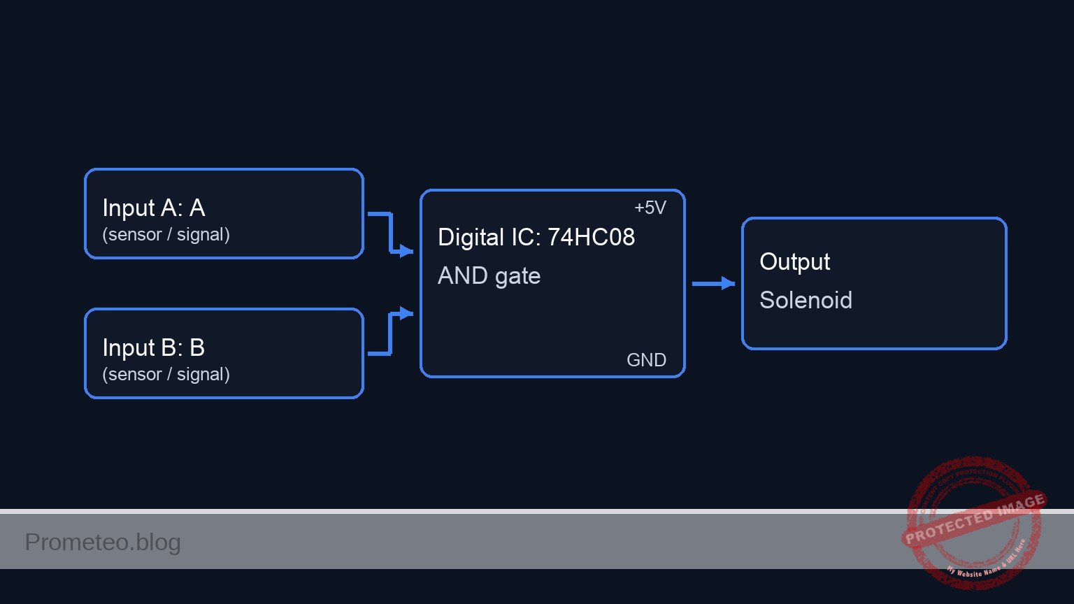
Schematic
[ INPUT SENSORS ]              [ LOGIC PROCESSING ]               [ OUTPUT ACTUATORS ]

                                                                     (Visual Status)
    [ Switch S1 ]                  +----------------+          +---> [ Resistor R4 ] --> [ LED D2 ] --> GND
    (w/ R1 Pull-down) --(Node VA)->|  Pin 1         |          |
                                   |                |          |
                                   |   U1: 74HC08   |--(V_GATE)+
                                   |   (AND Gate)   |  (Pin 3) |
                                   |                |          |
    [ Switch S2 ]                  |  Pin 2         |          |     (Solenoid Driver)
    (w/ R2 Pull-down) --(Node VB)->|                |          +---> [ Resistor R3 ] --> [ Transistor Q1 ]
                                   +----------------+                                         |
                                                                                         (Collector)
                                                                                              |
                                                                                              V
                                                                                     [ Solenoid L1 + Diode D1 ]
                                                                                     (Connected to VCC)
Truth table
This table describes the logic state of the 74HC08 output and the physical state of the solenoid.
| Input A (S1) | Input B (S2) | Output Y (V_GATE) | Solenoid State |
|---|---|---|---|
| 0 (Low) | 0 (Low) | 0 (Low) | Locked (OFF) |
| 0 (Low) | 1 (High) | 0 (Low) | Locked (OFF) |
| 1 (High) | 0 (Low) | 0 (Low) | Locked (OFF) |
| 1 (High) | 1 (High) | 1 (High) | Unlocked (ON) |
Measurements and tests
- Idle Check: With both switches OFF, measure voltage at V_GATE. It should be near 0 V. The solenoid should be relaxed.
- Partial Activation: Turn ON S1 only. Measure voltage at VA (should be 5 V) and VB (should be 0 V). Ensure V_GATE remains 0 V.
- Full Activation: Turn ON both S1 and S2.
- Measure V_GATE: It must read ~5 V (Logic High).
- Observe L1: The solenoid should retract/click.
- Measure voltage at V_LOCK: It should drop close to 0 V (saturation voltage of Q1), allowing current to flow from VCC through the solenoid.
- Current Draw: Measure the current flowing out of V1. It should increase significantly (e.g., +100mA depending on the solenoid) only when both inputs are High.
SPICE netlist and simulation
Reference SPICE Netlist (ngspice) — excerptFull SPICE netlist (ngspice)
* Simple security code validation

* ==============================================================================
* POWER SUPPLY
* ==============================================================================
V1 VCC 0 DC 5

* ==============================================================================
* INPUT STAGE (Switches & Pull-downs)
* ==============================================================================
* Note: S1 and S2 are simulated using Pulse Voltage Sources to generate
* dynamic logic patterns for validation.
* R1 and R2 are included as physical pull-down resistors per BOM.

* Input A (S1)
* Generates a pulse: Low for 0.5ms, High for 1ms, Period 2ms
V_S1 VA 0 PULSE(0 5 0.5m 1u 1u 1m 2m)
R1 VA 0 10k

* Input B (S2)
* Generates a pulse: High for 2ms, Low for 2ms, Period 4ms
V_S2 VB 0 PULSE(0 5 0 1u 1u 2m 4m)
R2 VB 0 10k

* ==============================================================================
* LOGIC STAGE (U1: 74HC08 Quad AND Gate)
* ==============================================================================
* Subcircuit to model one gate of the 74HC08, exposing power pins.
* Uses continuous behavioral modeling (sigmoid) for convergence.
.subckt 74HC08_GATE IN1 IN2 OUT VCC_PIN GND_PIN
* ... (truncated in public view) ...
Copy this content into a .cir file and run with ngspice.
* Simple security code validation

* ==============================================================================
* POWER SUPPLY
* ==============================================================================
V1 VCC 0 DC 5

* ==============================================================================
* INPUT STAGE (Switches & Pull-downs)
* ==============================================================================
* Note: S1 and S2 are simulated using Pulse Voltage Sources to generate
* dynamic logic patterns for validation.
* R1 and R2 are included as physical pull-down resistors per BOM.

* Input A (S1)
* Generates a pulse: Low for 0.5ms, High for 1ms, Period 2ms
V_S1 VA 0 PULSE(0 5 0.5m 1u 1u 1m 2m)
R1 VA 0 10k

* Input B (S2)
* Generates a pulse: High for 2ms, Low for 2ms, Period 4ms
V_S2 VB 0 PULSE(0 5 0 1u 1u 2m 4m)
R2 VB 0 10k

* ==============================================================================
* LOGIC STAGE (U1: 74HC08 Quad AND Gate)
* ==============================================================================
* Subcircuit to model one gate of the 74HC08, exposing power pins.
* Uses continuous behavioral modeling (sigmoid) for convergence.
.subckt 74HC08_GATE IN1 IN2 OUT VCC_PIN GND_PIN
B_AND OUT GND_PIN V = V(VCC_PIN) * (1 / (1 + exp(-20*(V(IN1)-2.5)))) * (1 / (1 + exp(-20*(V(IN2)-2.5))))
.ends

* Instantiate U1 (only one gate used: Inputs 1A, 1B -> Output 1Y)
* Pin 1=VA, Pin 2=VB, Pin 3=V_GATE, Pin 14=VCC, Pin 7=0 (GND)
XU1 VA VB V_GATE VCC 0 74HC08_GATE

* ==============================================================================
* INDICATOR STAGE
* ==============================================================================
* R4 limits current to LED D2
R4 V_GATE LED_A 330
D2 LED_A 0 LED_GREEN

* ==============================================================================
* OUTPUT STAGE (Actuator Driver)
* ==============================================================================
* Base resistor
R3 V_GATE Q1_B 1k

* Transistor Q1 (2N2222)
* Collector -> V_LOCK, Base -> Q1_B, Emitter -> 0
Q1 V_LOCK Q1_B 0 2N2222

* Solenoid L1 (Modeled as Inductor + Series Resistor)
* 5V / 100mA = 50 Ohm DC resistance. Inductance approx 10mH.
* Connected between VCC and V_LOCK.
R_L1 VCC INT_SOL 50
L1 INT_SOL V_LOCK 10mH

* Flyback Diode D1
* Cathode to VCC, Anode to V_LOCK
D1 V_LOCK VCC 1N4007

* ==============================================================================
* MODELS
* ==============================================================================
.model 2N2222 NPN (IS=1E-14 BF=200 VAF=100 CJC=8p CJE=25p TR=400n TF=1n)
.model 1N4007 D (IS=1N RS=0.1 BV=1000 IBV=10u N=1.7)
.model LED_GREEN D (IS=1e-22 RS=5 N=1.5 BV=5 IBV=10u CJO=10p)

* ==============================================================================
* SIMULATION COMMANDS
* ==============================================================================
.op
.tran 10u 5m

* Print logic states and output voltage
.print tran V(VA) V(VB) V(V_GATE) V(V_LOCK)

.end
Simulation Results (Transient Analysis)

Show raw data table (4960 rows)
Index   time            v(va)           v(vb)           v(v_gate)
0	0.000000e+00	0.000000e+00	0.000000e+00	1.860038e-43
1	1.000000e-08	0.000000e+00	5.000000e-02	3.720076e-43
2	2.000000e-08	0.000000e+00	1.000000e-01	1.011221e-42
3	4.000000e-08	0.000000e+00	2.000000e-01	4.123178e-42
4	8.000000e-08	0.000000e+00	4.000000e-01	5.077732e-41
5	1.600000e-07	0.000000e+00	8.000000e-01	4.990226e-39
6	3.200000e-07	0.000000e+00	1.600000e+00	2.809846e-35
7	6.400000e-07	0.000000e+00	3.200000e+00	4.846845e-28
8	1.000000e-06	0.000000e+00	5.000000e+00	9.644030e-22
9	1.064000e-06	0.000000e+00	5.000000e+00	9.643749e-22
10	1.192000e-06	0.000000e+00	5.000000e+00	9.643749e-22
11	1.448000e-06	0.000000e+00	5.000000e+00	9.643749e-22
12	1.960000e-06	0.000000e+00	5.000000e+00	9.643749e-22
13	2.984000e-06	0.000000e+00	5.000000e+00	9.643749e-22
14	5.032000e-06	0.000000e+00	5.000000e+00	9.643749e-22
15	9.128000e-06	0.000000e+00	5.000000e+00	9.643749e-22
16	1.732000e-05	0.000000e+00	5.000000e+00	9.643749e-22
17	2.732000e-05	0.000000e+00	5.000000e+00	9.643749e-22
18	3.732000e-05	0.000000e+00	5.000000e+00	9.643749e-22
19	4.732000e-05	0.000000e+00	5.000000e+00	9.643749e-22
20	5.732000e-05	0.000000e+00	5.000000e+00	9.643749e-22
21	6.732000e-05	0.000000e+00	5.000000e+00	9.643749e-22
22	7.732000e-05	0.000000e+00	5.000000e+00	9.643749e-22
23	8.732000e-05	0.000000e+00	5.000000e+00	9.643749e-22
... (4936 more rows) ...
Common mistakes and how to avoid them
- Floating Inputs: Forgetting resistors R1 or R2 causes the inputs to «float,» leading to erratic triggering of the lock caused by static electricity. Always use pull-down resistors with CMOS logic like the 74HC series.
- Driving Solenoid Directly: Connecting the solenoid directly to the 74HC08 output pin (pin 3). The chip can only supply ~20mA, while a solenoid needs >100mA. This will destroy the chip. Always use a transistor driver (Q1).
- Omitting the Flyback Diode: Forgetting D1 across the solenoid. When the solenoid turns off, it generates a high-voltage spike (back EMF) that destroys the transistor instantly.
Troubleshooting
- Solenoid does not activate but LED works: The logic is correct, but the drive capability is insufficient. Check Q1 connections and ensure the solenoid power requirement matches the supply.
- Logic Gate gets hot: You might have shorted the output pin to ground or are trying to drive the solenoid directly. Disconnect immediately and check the wiring of pin 3.
- Circuit works inversely (Unlocks when switches are OFF): You may have wired the pull-down resistors as pull-ups or connected the transistor to the wrong rail. Verify R1 and R2 go to Ground.
- Input A triggers the lock without Input B: Check for a short circuit between pin 1 and pin 2, or check if pin 2 is accidentally connected to VCC.
Possible improvements and extensions
- Add a Timer: Feed the output of the 74HC08 into a 555 Timer (Monostable mode) so the lock stays open for 5 seconds even if the user releases the switches immediately.
- Expand Security: Cascade a second 74HC08 to add a third switch (Switch A AND Switch B AND Switch C) for higher security.
More Practical Cases on Prometeo.blog
Find this product and/or books on this topic on Amazon
As an Amazon Associate, I earn from qualifying purchases. If you buy through this link, you help keep this project running.
Quick Quiz

Telecommunications Electronics Engineer and Computer Engineer (official degrees in Spain).

