

Level: Basic. Build an off-delay circuit using the slow discharge of a capacitor to control a transistor.
Objective and use case
In this session, you will build an analog timer circuit that keeps an LED illuminated for a specific duration after a push-button is released. This demonstrates how a capacitor stores energy and discharges it over time to control a switching element (the transistor).
Why it is useful:
* Interior car lighting: Lights that fade out slowly after the door is closed.
* Staircase timers: Lighting that remains on long enough for someone to climb the stairs.
* Bathroom fans: Fans that continue running for a few minutes after being switched off to clear humidity.
* Debouncing: Smoothing out short, unwanted signal interruptions.
Expected outcome:
* Button Press: The LED turns ON immediately to full brightness.
* Button Release: The LED remains ON initially.
* Delay Phase: The LED gradually dims and turns OFF after a few seconds as the capacitor voltage drops.
* Target Audience: Students and hobbyists learning about RC time constants and transistor switching.
Materials
- V1: 9 V DC supply, function: main power source.
- S1: Push-button (Normally Open), function: charging trigger.
- C1: 470 µF electrolytic capacitor, function: timing and energy storage.
- R1: 10 kΩ resistor, function: discharge timing resistor.
- R2: 470 Ω resistor, function: LED current limiting.
- Q1: 2N2222 NPN transistor, function: current switch.
- D1: Red LED, function: visual output indicator.
Wiring guide
Construct the circuit following these connections using the specific node names provided.
-
Power Supply:
- Connect V1 positive terminal to node
VCC. - Connect V1 negative terminal to node
0(GND).
- Connect V1 positive terminal to node
-
Input and Timing Network:
- Connect S1 between node
VCCand nodeVCAP. - Connect C1 positive terminal to node
VCAP. - Connect C1 negative terminal to node
0. - Connect R1 between node
VCAPand nodeBASE.
- Connect S1 between node
-
Transistor Switch:
- Connect Q1 Base to node
BASE. - Connect Q1 Emitter to node
0. - Connect Q1 Collector to node
COL.
- Connect Q1 Base to node
-
Output Load (LED):
- Connect R2 between node
VCCand nodeLED_A. - Connect D1 Anode to node
LED_A. - Connect D1 Cathode to node
COL.
- Connect R2 between node
Conceptual block diagram
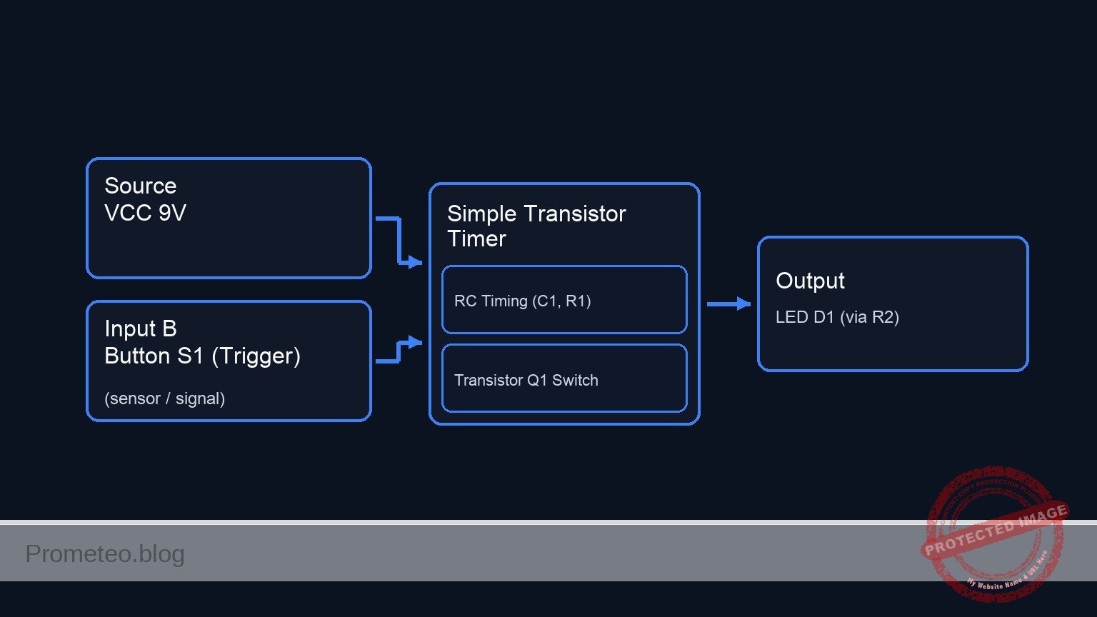
Schematic
[ INPUT & TIMING ]                  [ LOGIC / SWITCH ]                 [ OUTPUT LOAD ]

(VCC 9 V) --+--(Power Path)--------------------------------------------------> [ Resistor R2 ]
           |                                                                        |
           |                                                                        v
     [ Button S1 ]                                                             [ LED D1 ]
           |                                                                        |
           v (Trigger)                                                              |
     [ Node VCAP ] --(Slow Discharge)--> [ Resistor R1 ] --(Base Sig)-->+           |
           |                                                            |           |
           + <--(Stores Charge)-- [ Capacitor C1 ]                      |           |
                                       |                                v           v
                                       v                        +-----------------------+
                                    [ GND ]                     |     TRANSISTOR Q1     |
                                                                | (Base)    (Collector) |
                                                                +-----------------------+
                                                                            |
                                                                            v (Emitter)
                                                                         [ GND ]
Measurements and tests
Follow these steps to validate the circuit behavior using a multimeter.
- Initial State: Ensure S1 is not pressed. The LED should be OFF.
- Measure voltage at
VCAP. It should be near 0 V.
- Measure voltage at
- Charging Phase: Press and hold S1.
- Check: The LED turns ON immediately.
- Measurement: The voltage at
VCAPshould instantly rise to approximately 9 V (VCC).
- Discharge Phase: Release S1 and start a stopwatch.
- Observation: The LED remains lit.
- Measurement: Monitor the voltage at
VCAP. It will slowly decrease. - Threshold: When
VCAPdrops below approximately 1.4 V (V_BE + drop across R1), the LED will dim significantly and turn OFF.
- Time Constant: Record the time from release until the LED turns completely off.
SPICE netlist and simulation
Reference SPICE Netlist (ngspice) — excerptFull SPICE netlist (ngspice)
* Practical case: Simple Transistor Timer

* --- Power Supply ---
* V1: 9 V DC supply
V1 VCC 0 DC 9

* --- Input and Timing Network ---
* S1: Push-button (Normally Open)
* Modeled as a Voltage Controlled Switch (S1) driven by a control pulse (V_S1_ACT)
* Connects VCC to VCAP when activated
S1 VCC VCAP CTRL 0 SW_MODEL

* Control signal for the button press simulation
* Press button at T=0.5s, hold for 0.5s, then release to allow discharge
V_S1_ACT CTRL 0 PULSE(0 5 0.5 1m 1m 0.5 20)

* C1: 470 µF electrolytic capacitor
C1 VCAP 0 470u

* R1: 10 kΩ resistor (Discharge path to Base)
* ... (truncated in public view) ...
Copy this content into a .cir file and run with ngspice.
* Practical case: Simple Transistor Timer

* --- Power Supply ---
* V1: 9 V DC supply
V1 VCC 0 DC 9

* --- Input and Timing Network ---
* S1: Push-button (Normally Open)
* Modeled as a Voltage Controlled Switch (S1) driven by a control pulse (V_S1_ACT)
* Connects VCC to VCAP when activated
S1 VCC VCAP CTRL 0 SW_MODEL

* Control signal for the button press simulation
* Press button at T=0.5s, hold for 0.5s, then release to allow discharge
V_S1_ACT CTRL 0 PULSE(0 5 0.5 1m 1m 0.5 20)

* C1: 470 µF electrolytic capacitor
C1 VCAP 0 470u

* R1: 10 kΩ resistor (Discharge path to Base)
R1 VCAP BASE 10k

* --- Transistor Switch ---
* Q1: 2N2222 NPN transistor
* Connections: Collector=COL, Base=BASE, Emitter=0(GND)
Q1 COL BASE 0 2N2222MOD

* --- Output Load (LED) ---
* R2: 470 Ω resistor
R2 VCC LED_A 470

* D1: Red LED
* Connections: Anode=LED_A, Cathode=COL
D1 LED_A COL DLED

* --- Models ---
* Switch Model: Threshold 2.5V, Low On-Resistance
.model SW_MODEL SW(Vt=2.5 Ron=0.1 Roff=100Meg)

* NPN Transistor Model (Generic 2N2222)
.model 2N2222MOD NPN(IS=1E-14 VAF=100 BF=200 IKF=0.3 XTB=1.5 BR=3 CJC=8E-12 CJE=25E-12 TR=46.91E-9 TF=411.1E-12 ITF=0.6 VTF=1.7 XTF=3 RB=10 RC=0.3 RE=0.2)

* LED Model (Red LED approx)
.model DLED D(IS=1u N=2 RS=10 BV=5 IBV=10u)

* --- Analysis Commands ---
* Transient analysis for 10 seconds to observe the long RC discharge (Tau ~ 4.7s)
.tran 10m 10s

* Output voltage of Capacitor, Base, Collector, and LED Anode
.print tran V(VCAP) V(BASE) V(COL) V(LED_A)

.op
.end
Simulation Results (Transient Analysis)

Show raw data table (2110 rows)
Index   time            v(vcap)         v(base)         v(col)
0	0.000000e+00	5.504285e-01	5.495835e-01	8.838023e+00
1	1.000000e-04	5.504285e-01	5.495836e-01	8.838088e+00
2	2.000000e-04	5.504285e-01	5.495835e-01	8.838088e+00
3	4.000000e-04	5.504285e-01	5.495835e-01	8.838088e+00
4	8.000000e-04	5.504285e-01	5.495835e-01	8.838088e+00
5	1.600000e-03	5.504285e-01	5.495835e-01	8.838088e+00
6	3.200000e-03	5.504285e-01	5.495835e-01	8.838088e+00
7	6.400000e-03	5.504285e-01	5.495835e-01	8.838088e+00
8	1.280000e-02	5.504285e-01	5.495835e-01	8.838088e+00
9	2.280000e-02	5.504285e-01	5.495835e-01	8.838088e+00
10	3.280000e-02	5.504285e-01	5.495835e-01	8.838088e+00
11	4.280000e-02	5.504285e-01	5.495835e-01	8.838088e+00
12	5.280000e-02	5.504285e-01	5.495835e-01	8.838088e+00
13	6.280000e-02	5.504285e-01	5.495835e-01	8.838088e+00
14	7.280000e-02	5.504285e-01	5.495835e-01	8.838088e+00
15	8.280000e-02	5.504285e-01	5.495835e-01	8.838088e+00
16	9.280000e-02	5.504285e-01	5.495835e-01	8.838088e+00
17	1.028000e-01	5.504285e-01	5.495835e-01	8.838088e+00
18	1.128000e-01	5.504285e-01	5.495835e-01	8.838088e+00
19	1.228000e-01	5.504285e-01	5.495835e-01	8.838088e+00
20	1.328000e-01	5.504285e-01	5.495835e-01	8.838088e+00
21	1.428000e-01	5.504285e-01	5.495835e-01	8.838088e+00
22	1.528000e-01	5.504285e-01	5.495835e-01	8.838088e+00
23	1.628000e-01	5.504285e-01	5.495835e-01	8.838088e+00
... (2086 more rows) ...
Common mistakes and how to avoid them
- Reversed Capacitor Polarity: Electrolytic capacitors can explode or fail if connected backwards. Ensure the negative stripe on C1 connects to
0(GND). - Incorrect Transistor Pinout: Confusing the Collector and Emitter prevents switching. Verify the 2N2222 datasheet; usually, the tab or flat side indicates the pin orientation.
- Capacitor Value Too Small: Using a small capacitor (e.g., 100 nF) results in a delay too short for the human eye to perceive. Use at least 100 µF for visible results.
Troubleshooting
- Symptom: LED never turns ON.
- Cause: LED installed backwards or transistor broken.
- Fix: Check D1 orientation (Anode to resistor, Cathode to Collector) and verify Q1 connections.
- Symptom: LED turns OFF immediately upon releasing the button.
- Cause: Capacitor is missing, disconnected, or value is too low.
- Fix: Ensure C1 is firmly connected between
VCAPand0. Try increasing C1 to 1000 µF.
- Symptom: Transistor gets very hot.
- Cause: Missing base resistor or short circuit at the output.
- Fix: Ensure R1 (10 kΩ) is correctly installed between the capacitor and the base to limit base current.
Possible improvements and extensions
- Variable Timer: Replace R1 with a 50 kΩ potentiometer in series with a 1 kΩ resistor to allow the user to adjust the delay duration.
- Darlington Pair: Replace Q1 with a Darlington transistor (or two NPNs connected as a Darlington pair) to significantly increase input impedance, allowing for much longer delays with the same capacitor value.
More Practical Cases on Prometeo.blog
Find this product and/or books on this topic on Amazon
As an Amazon Associate, I earn from qualifying purchases. If you buy through this link, you help keep this project running.
Quick Quiz

Telecommunications Electronics Engineer and Computer Engineer (official degrees in Spain).

