

Level: Basic. Objective: Understand BJT cut-off and saturation to control a load (LED) with a small control signal.
Objective and use case
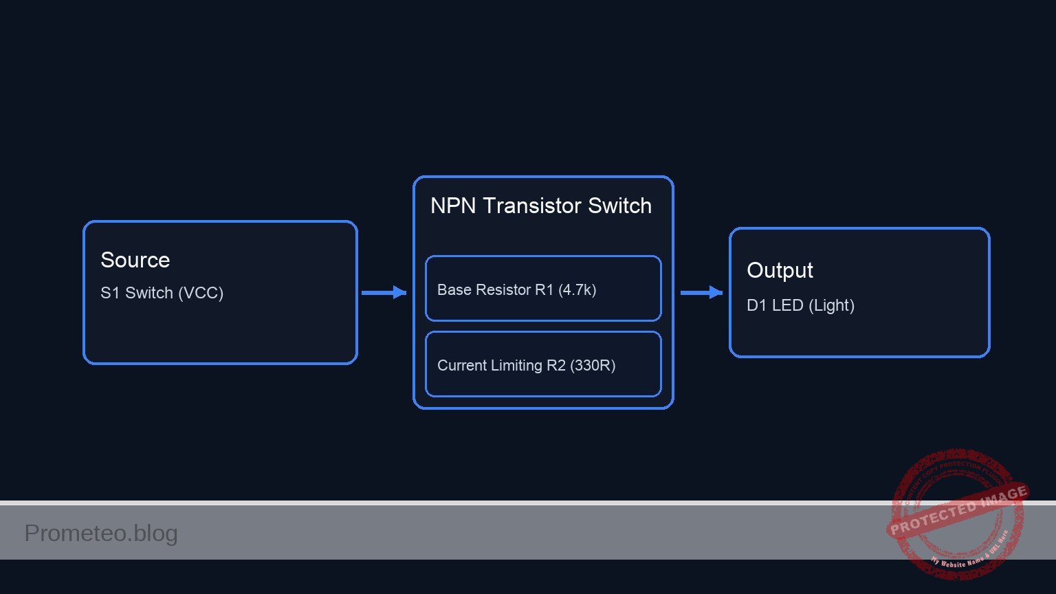
In this practical case, you will build a circuit using an NPN Bipolar Junction Transistor (BJT) to switch a high-current load (an LED) on and off using a low-current control signal triggered by a push button.
Why it is useful:
* Microcontroller interfacing: Allows low-power pins (like those on an Arduino or ESP32) to drive higher current loads.
* Sensor actuation: Enables weak signals from sensors (like LDRs or thermistors) to activate lights or alarms.
* Component protection: Separates the sensitive control circuit from the power circuit.
* Logic switching: Forms the fundamental building block of digital logic gates.
Expected outcome:
* Idle State (Button Released): The transistor is in Cut-off. IC ≈ 0 mA, LED is OFF, and VCE ≈ Vsupply.
* Active State (Button Pressed): The transistor enters Saturation. LED is ON.
* Saturation Voltage: VCE drops to approximately $0.1$ V to $0.2$ V.
* Base Threshold: VBE stabilizes around $0.7$ V when the transistor is conducting.
Target audience: Basic level electronics students.
Materials
- V1: 9 V DC battery or power supply, function: Main circuit power.
- S1: Tactile Push-button (Normally Open), function: User input trigger.
- R1: 10 kΩ resistor, function: Base current limiting (to ensure saturation without damaging the Base).
- R2: 100 kΩ resistor, function: Pull-down resistor (keeps Base at 0 V when S1 is open).
- R3: 330 Ω resistor, function: LED current limiting protection.
- Q1: 2N2222 (or BC547) NPN Transistor, function: Electronic switch.
- D1: Red LED, function: Visual load indicator.
Wiring guide
This guide uses specific node names to help you visualize the connections.
* Power Nodes: Connect V1 positive to node VCC and negative to node 0 (GND).
* Input Stage:
* Connect one side of S1 to VCC.
* Connect the other side of S1 to node INPUT_SIG.
* Connect R1 (10 kΩ) between INPUT_SIG and node BASE.
* Connect R2 (100 kΩ) between node BASE and node 0 (GND).
* Transistor Connections:
* Connect the Base of Q1 to node BASE.
* Connect the Emitter of Q1 directly to node 0 (GND).
* Connect the Collector of Q1 to node COLL.
* Output Load:
* Connect R3 (330 Ω) between VCC and node LED_ANODE.
* Connect the Anode (long leg) of D1 to node LED_ANODE.
* Connect the Cathode (short leg, flat side) of D1 to node COLL.
Conceptual block diagram
Schematic
Title: Practical case: The transistor as a light switch

1. CONTROL PATH (Input Stage)
   Flow: VCC triggers the Base when S1 is pressed. R2 ensures Base is 0 V when S1 is open.

   [ VCC ] --> [ S1: Button ] --(INPUT_SIG)--> [ R1: 10k ] --(BASE)--+--> [ Q1: Base ]
                                                                     |
                                                                     +--> [ R2: 100k ] --> [ GND ]

2. LOAD PATH (Output Stage)
   Flow: Current flows from VCC through the LED into the Transistor Collector.

   [ VCC ] --> [ R3: 330R ] --(LED_ANODE)--> [ D1: Red LED ] --(COLL)--> [ Q1: Collector ]

3. COMMON RETURN (Grounding)
   Flow: The transistor completes the circuit to Ground.

   [ Q1: Emitter ] --> [ GND ]
Measurements and tests
Perform these steps with a multimeter to verify the transistor regions of operation.
-
Test Cut-off Region (Switch Open):
- Ensure S1 is not pressed.
- Measure voltage between Base and Emitter (VBE). Result should be 0 V.
- Measure voltage between Collector and Emitter (VCE). Result should be close to 9 V (Source voltage), indicating the switch is open.
- Observe D1: It must be OFF.
-
Test Saturation Region (Switch Closed):
- Press and hold S1.
- Measure voltage between Base and Emitter (VBE). Result should be approximately 0.65 V to 0.75 V.
- Measure voltage between Collector and Emitter (VCE). Result should drop to < 0.2 V. This voltage drop proves the transistor is acting as a closed switch (Saturation).
- Observe D1: It must turn ON brightly.
SPICE netlist and simulation
Reference SPICE Netlist (ngspice) — excerptFull SPICE netlist (ngspice)
* Practical case: The transistor as a light switch
* Improved Netlist with robust switch modelling

.width out=256

* --- Power Supply ---
* V1: 9 V DC battery (Main circuit power)
V1 VCC 0 DC 9

* --- User Input Trigger (S1) ---
* S1: Tactile Push-button (Normally Open) connecting VCC to INPUT_SIG.
* Modeled using a Voltage-Controlled Switch (S1) driven by a control pulse (V_ACT).
* V_ACT simulates the user pressing the button (Logic 0 -> 1 -> 0).
V_ACT ACTUATE 0 PULSE(0 5 1ms 100u 100u 5ms 20ms)
S1 VCC INPUT_SIG ACTUATE 0 SW_TACTILE

* --- Input Stage ---
* R1: 10 kOhm, Base current limiting
R1 INPUT_SIG BASE 10k

* ... (truncated in public view) ...
Copy this content into a .cir file and run with ngspice.
* Practical case: The transistor as a light switch
* Improved Netlist with robust switch modelling

.width out=256

* --- Power Supply ---
* V1: 9 V DC battery (Main circuit power)
V1 VCC 0 DC 9

* --- User Input Trigger (S1) ---
* S1: Tactile Push-button (Normally Open) connecting VCC to INPUT_SIG.
* Modeled using a Voltage-Controlled Switch (S1) driven by a control pulse (V_ACT).
* V_ACT simulates the user pressing the button (Logic 0 -> 1 -> 0).
V_ACT ACTUATE 0 PULSE(0 5 1ms 100u 100u 5ms 20ms)
S1 VCC INPUT_SIG ACTUATE 0 SW_TACTILE

* --- Input Stage ---
* R1: 10 kOhm, Base current limiting
R1 INPUT_SIG BASE 10k

* R2: 100 kOhm, Pull-down resistor (keeps Base low when S1 is open)
R2 BASE 0 100k

* --- Transistor Switch ---
* Q1: 2N2222 NPN Transistor
* Connections: Collector=COLL, Base=BASE, Emitter=0(GND)
Q1 COLL BASE 0 2N2222

* --- Output Load ---
* R3: 330 Ohm, LED current limiting resistor
R3 VCC LED_ANODE 330

* D1: Red LED
* Connections: Anode=LED_ANODE, Cathode=COLL
D1 LED_ANODE COLL RED_LED

* --- Component Models ---
* Switch Model: Added hysteresis (Vh) and relaxed Ron for better convergence
.model SW_TACTILE SW(Vt=2.5 Vh=0.1 Ron=1 Roff=100Meg)

* Transistor Model: Standard 2N2222 parameters
.model 2N2222 NPN(IS=1E-14 VAF=100 BF=200 IKF=0.3 XTB=1.5 BR=3 CJC=8p CJE=25p TR=46.9n TF=411p ITF=0.6 VTF=1.7 XTF=3 RB=10 RC=1 RE=0.1)

* LED Model: Generic Red LED parameters
.model RED_LED D(IS=93.2p RS=42m N=3.73 BV=5 IBV=10u CJO=2.97p VJ=0.75 M=0.33 TT=4.32u)

* --- Analysis Commands ---
.op
* Simulate for 10ms to capture the button press event
.tran 100u 10ms

* --- Output Directives ---
* Printing INPUT (Switch output) and OUTPUT (Collector voltage) first
.print tran V(INPUT_SIG) V(COLL) V(BASE) V(LED_ANODE) V(ACTUATE)

.end
Simulation Results (Transient Analysis)

Show raw data table (170 rows)
Index   time            v(input_sig)    v(coll)         v(base)         v(led_anode)    v(actuate)
0	0.000000e+00	9.890018e-03	8.982941e+00	8.991007e-03	9.000000e+00	0.000000e+00
1	1.000000e-06	9.890019e-03	8.982941e+00	8.991008e-03	9.000000e+00	0.000000e+00
2	2.000000e-06	9.890019e-03	8.982941e+00	8.991008e-03	9.000000e+00	0.000000e+00
3	4.000000e-06	9.890021e-03	8.982941e+00	8.991010e-03	9.000000e+00	0.000000e+00
4	8.000000e-06	9.890021e-03	8.982941e+00	8.991010e-03	9.000000e+00	0.000000e+00
5	1.600000e-05	9.890021e-03	8.982941e+00	8.991010e-03	9.000000e+00	0.000000e+00
6	3.200000e-05	9.890021e-03	8.982941e+00	8.991010e-03	9.000000e+00	0.000000e+00
7	6.400000e-05	9.890021e-03	8.982942e+00	8.991010e-03	9.000000e+00	0.000000e+00
8	1.280000e-04	9.890021e-03	8.982942e+00	8.991010e-03	9.000000e+00	0.000000e+00
9	2.280000e-04	9.890021e-03	8.982943e+00	8.991010e-03	9.000000e+00	0.000000e+00
10	3.280000e-04	9.890021e-03	8.982944e+00	8.991010e-03	9.000000e+00	0.000000e+00
11	4.280000e-04	9.890021e-03	8.982945e+00	8.991010e-03	9.000000e+00	0.000000e+00
12	5.280000e-04	9.890021e-03	8.982946e+00	8.991010e-03	9.000000e+00	0.000000e+00
13	6.280000e-04	9.890021e-03	8.982947e+00	8.991010e-03	9.000000e+00	0.000000e+00
14	7.280000e-04	9.890021e-03	8.982948e+00	8.991010e-03	9.000000e+00	0.000000e+00
15	8.280000e-04	9.890021e-03	8.982949e+00	8.991010e-03	9.000000e+00	0.000000e+00
16	9.280000e-04	9.890021e-03	8.982950e+00	8.991010e-03	9.000000e+00	0.000000e+00
17	1.000000e-03	9.890021e-03	8.982950e+00	8.991010e-03	9.000000e+00	0.000000e+00
18	1.010000e-03	9.890021e-03	8.982951e+00	8.991010e-03	9.000000e+00	5.000000e-01
19	1.027500e-03	9.890021e-03	8.982951e+00	8.991010e-03	9.000000e+00	1.375000e+00
20	1.032344e-03	9.890021e-03	8.982951e+00	8.991010e-03	9.000000e+00	1.617187e+00
21	1.040820e-03	9.890021e-03	8.982951e+00	8.991010e-03	9.000000e+00	2.041016e+00
22	1.043167e-03	9.890021e-03	8.982951e+00	8.991010e-03	9.000000e+00	2.158325e+00
23	1.047272e-03	9.890021e-03	8.982951e+00	8.991010e-03	9.000000e+00	2.363617e+00
... (146 more rows) ...
Common mistakes and how to avoid them
- Swapping Collector and Emitter:
- Error: The LED turns on but looks dim or fails to switch completely. The transistor may overheat.
- Solution: Double-check the pinout of the 2N2222 (E-B-C or C-B-E depending on the specific package/datasheet).
- Omitting the Base Resistor (R1):
- Error: Connecting the switch directly to the Base causes a massive current flow from Base to Emitter, destroying the transistor instantly.
- Solution: Always include a limiting resistor (R1) in series with the Base.
- Floating Base (Missing R2):
- Error: The LED might flicker or glow faintly when the switch is open because the Base picks up electromagnetic noise.
- Solution: Ensure R2 (Pull-down) is connected to ground to discharge the Base capacitance when the switch is open.
Troubleshooting
- Symptom: LED is always ON, even when the button is not pressed.
- Cause: Transistor C-E shorted internally or R2 is missing/disconnected.
- Fix: Replace Q1 and check R2 connection to Ground.
- Symptom: LED does not turn ON when button is pressed.
- Cause: LED connected backwards, R1 value too high (preventing saturation), or R3 too high.
- Fix: Check LED polarity. Verify R1 is 10 kΩ and R3 is 330 Ω.
- Symptom: LED is very dim when ON.
- Cause: Transistor is in the «Active» region, not «Saturation».
- Fix: Decrease R1 slightly (e.g., to 4.7 kΩ) to increase Base current (IB) and force full saturation.
Possible improvements and extensions
- High Power Control: Replace the LED and R3 with a 9 V Relay (remember to add a flyback diode in parallel with the relay coil) to control a household lamp.
- Automatic Night Light: Replace the tactile button (S1) with an LDR (Light Dependent Resistor) and adjust the position of resistors to create a sensor that turns on the LED in the dark.
More Practical Cases on Prometeo.blog
Find this product and/or books on this topic on Amazon
As an Amazon Associate, I earn from qualifying purchases. If you buy through this link, you help keep this project running.
Quick Quiz

Telecommunications Electronics Engineer and Computer Engineer (official degrees in Spain).

