

Level: Basic. Analyzing the instability caused by improper voltage divider inputs on digital gates.
Objective and use case
In this practical case, you will build a circuit where the input to a digital inverter (NOT gate) is held at exactly 2.5 V using a symmetrical voltage divider. This creates a «forbidden» state for 5 V logic families.
- Understanding Logic Thresholds: Learn why digital inputs need defined High and Low voltages, not just «something in the middle.»
- Diagnosing Instability: Recognize symptoms of undefined states, such as oscillation or excessive heating.
- Internal Transistor Behavior: Visualize what happens to the internal MOSFETs when the input voltage is in the «dead zone.»
Expected Outcome:
* Signal: The input voltage (Vin) measures exactly 2.5 V.
* Output: The Output LED may be dim, flickering, or stuck at an intermediate voltage (not fully 0 V or 5 V).
* Thermal: The 74HC04 chip may become slightly warm due to internal «shoot-through» current.
Target audience: Students dealing with sensor interfacing and logic levels.
Materials
- V1: 5 V DC supply, function: Main power source
- R1: 10 kΩ resistor, function: Top leg of voltage divider
- R2: 10 kΩ resistor, function: Bottom leg of voltage divider
- U1: 74HC04, function: Hex Inverter (NOT gate)
- R3: 330 Ω resistor, function: LED current limiting
- D1: Red LED, function: Logic state indicator
- C1: 100 nF capacitor, function: Power supply decoupling
Pin-out of the IC used
Chip: 74HC04 (Hex Inverter)
| Pin | Name | Logic Function | Connection in this case |
|---|---|---|---|
| 1 | 1 A | Input | Connected to Voltage Divider (2.5 V) |
| 2 | 1Y | Output | Connected to LED resistor |
| 7 | GND | Ground | Connected to Power Supply Ground |
| 14 | VCC | Power (+5 V) | Connected to Power Supply +5 V |
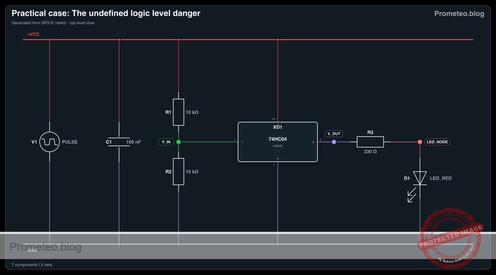
Wiring guide
- VCC: Connect positive terminal of V1, Pin 14 of U1, and one side of R1.
- 0 (GND): Connect negative terminal of V1, Pin 7 of U1, one side of R2, and the cathode (short leg) of D1.
- V_IN: Connect the remaining side of R1, the remaining side of R2, and Pin 1 (Input 1 A) of U1. Note: This node creates the problematic 2.5 V level.
- V_OUT: Connect Pin 2 (Output 1Y) of U1 to one side of R3.
- LED_NODE: Connect the remaining side of R3 to the anode (long leg) of D1.
- Decoupling: Connect C1 directly between Pin 14 and Pin 7 of U1.
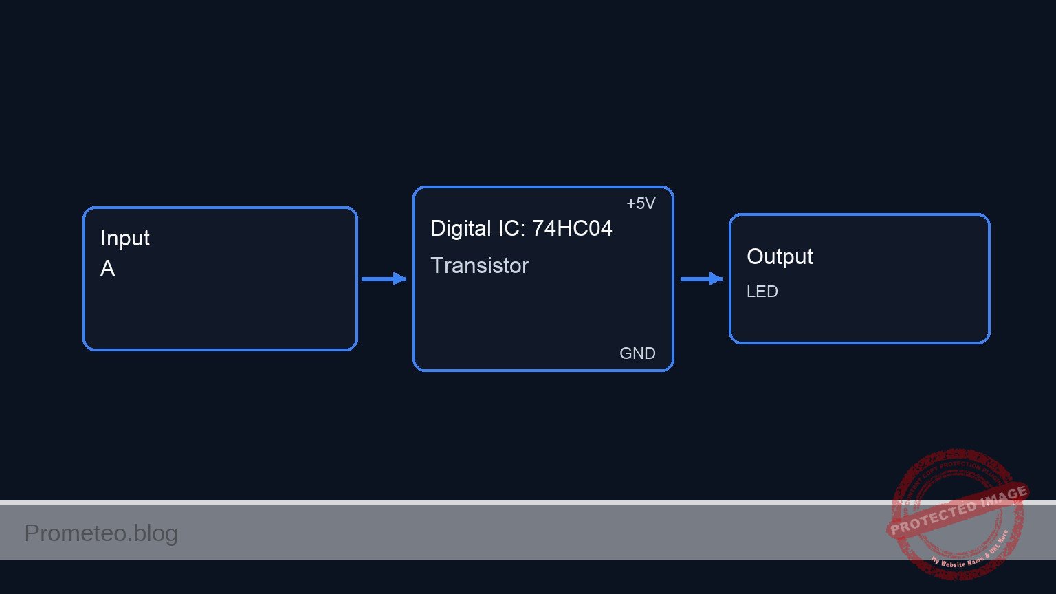
Conceptual block diagram
Schematic
INPUT STAGE (Voltage Divider)              PROCESSING STAGE (Logic)                  OUTPUT STAGE (Load)

VCC (5 V)
   |
[ R1: 10 kΩ ]
   |
   +---------(V_IN: ~2.5 V)---------> [ U1: 74HC04 (Inverter) ] -------(V_OUT)-------> [ R3: 330 Ω ] ----> [ D1: LED ] ----> GND
   |          (Undefined Level)      [ Input: Pin 1          ]
[ R2: 10 kΩ ]                         [ Output: Pin 2         ]
   |                                 [ Power: VCC/GND + C1   ]
GND (0 V)
Electrical diagram
Truth table
Gate: NOT (Inverter)
| Input (A) | Output (Y) |
|---|---|
| L (0 V) | H (5 V) |
| H (5 V) | L (0 V) |
| 2.5 V | Undefined / Unstable |
Measurements and tests
- Input Voltage Check: Set your multimeter to DC Voltage. Place the red probe on node V_IN (Pin 1 of U1) and the black probe on GND. Verify the reading is approximately 2.5 V.
- Output Observation: Look at D1. It might be glowing dimly or flickering. This indicates the output is not driving a solid Logic High or Low.
- Output Voltage Check: Measure the voltage at V_OUT (Pin 2). It will likely not be 0 V or 5 V, but a value in between, or it may be oscillating (fluctuating reading).
- Touch Test (Caution): Carefully touch the top of the plastic package of the 74HC04. If the chip feels warmer than ambient temperature, it is drawing excess current.
SPICE netlist and simulation
Reference SPICE Netlist (ngspice) — excerptFull SPICE netlist (ngspice)
* Practical case: The Undefined Logic Level Danger
.width out=256

* --- Models ---
* Generic Red LED Model
.model LED_RED D(IS=1e-22 N=1.5 RS=10 BV=5 CJO=50p IBV=1u)

* Subcircuit for U1: 74HC04 Hex Inverter
* Pinout: 1=Input(A), 2=Output(Y), 7=GND, 14=VCC
* Implemented with a continuous sigmoid function to allow robust simulation
* of the linear region (undefined state) without convergence issues.
.subckt 74HC04 1 2 7 14
B_INV 2 7 V = V(14,7) / (1 + exp(20 * (V(1,7) - 0.5*V(14,7))))
.ends

* --- Components ---

* V1: Main Power Supply
* Using PULSE to simulate power-on transient (0V to 5V)
V1 VCC 0 PULSE(0 5 1u 10u 10u 100m 200m)
* ... (truncated in public view) ...
Copy this content into a .cir file and run with ngspice.
* Practical case: The Undefined Logic Level Danger
.width out=256

* --- Models ---
* Generic Red LED Model
.model LED_RED D(IS=1e-22 N=1.5 RS=10 BV=5 CJO=50p IBV=1u)

* Subcircuit for U1: 74HC04 Hex Inverter
* Pinout: 1=Input(A), 2=Output(Y), 7=GND, 14=VCC
* Implemented with a continuous sigmoid function to allow robust simulation
* of the linear region (undefined state) without convergence issues.
.subckt 74HC04 1 2 7 14
B_INV 2 7 V = V(14,7) / (1 + exp(20 * (V(1,7) - 0.5*V(14,7))))
.ends

* --- Components ---

* V1: Main Power Supply
* Using PULSE to simulate power-on transient (0V to 5V)
V1 VCC 0 PULSE(0 5 1u 10u 10u 100m 200m)

* R1: Top leg of voltage divider (10k)
R1 VCC V_IN 10k

* R2: Bottom leg of voltage divider (10k)
* This creates approx 2.5V at V_IN when VCC is 5V
R2 V_IN 0 10k

* U1: 74HC04 Hex Inverter
* Connections: Pin 1=V_IN, Pin 2=V_OUT, Pin 7=0(GND), Pin 14=VCC
XU1 V_IN V_OUT 0 VCC 74HC04

* C1: Decoupling capacitor (100nF)
C1 VCC 0 100n

* R3: LED current limiting resistor (330 Ohm)
R3 V_OUT LED_NODE 330

* D1: Red LED
D1 LED_NODE 0 LED_RED

* --- Analysis ---

* Transient analysis to capture power-up and settling
* Step size 1us, Stop time 500us
.tran 1u 500u

* Print directives for simulation logging
.print tran V(V_IN) V(V_OUT) V(LED_NODE) V(VCC)

* Operating point calculation
.op

.end
Simulation Results (Transient Analysis)

Show raw data table (519 rows)
Index   time            v(v_in)         v(v_out)        v(led_node)     v(vcc)
0	0.000000e+00	0.000000e+00	0.000000e+00	-1.32954e-36	0.000000e+00
1	1.000000e-08	0.000000e+00	0.000000e+00	-8.37118e-37	0.000000e+00
2	2.000000e-08	0.000000e+00	0.000000e+00	-2.17031e-37	0.000000e+00
3	4.000000e-08	0.000000e+00	0.000000e+00	6.442019e-37	0.000000e+00
4	8.000000e-08	0.000000e+00	0.000000e+00	1.087387e-36	0.000000e+00
5	1.600000e-07	0.000000e+00	0.000000e+00	5.886649e-37	0.000000e+00
6	3.200000e-07	0.000000e+00	0.000000e+00	-7.16419e-38	0.000000e+00
7	6.400000e-07	0.000000e+00	0.000000e+00	-1.33719e-37	0.000000e+00
8	1.000000e-06	0.000000e+00	0.000000e+00	-1.75658e-38	0.000000e+00
9	1.005123e-06	1.280776e-03	1.280776e-03	3.255392e-04	2.561552e-03
10	1.015369e-06	3.842328e-03	3.842328e-03	1.418765e-03	7.684656e-03
11	1.035862e-06	8.965432e-03	8.965432e-03	5.258943e-03	1.793086e-02
12	1.070382e-06	1.759552e-02	1.759552e-02	1.345000e-02	3.519104e-02
13	1.105069e-06	2.626716e-02	2.626716e-02	2.210557e-02	5.253431e-02
14	1.174442e-06	4.361042e-02	4.361042e-02	3.941132e-02	8.722085e-02
15	1.313188e-06	7.829696e-02	7.829696e-02	7.402122e-02	1.565939e-01
16	1.590680e-06	1.476700e-01	1.476700e-01	1.432281e-01	2.953401e-01
17	2.145665e-06	2.864162e-01	2.864162e-01	2.815810e-01	5.728324e-01
18	3.145665e-06	5.364162e-01	5.364162e-01	5.305352e-01	1.072832e+00
19	4.145665e-06	7.864162e-01	7.864162e-01	7.789169e-01	1.572832e+00
20	5.145665e-06	1.036416e+00	1.036416e+00	1.027633e+00	2.072832e+00
21	6.145665e-06	1.286416e+00	1.286416e+00	1.276050e+00	2.572832e+00
22	7.145665e-06	1.536416e+00	1.536416e+00	1.521539e+00	3.072832e+00
23	8.145665e-06	1.786416e+00	1.786416e+00	1.662480e+00	3.572832e+00
... (495 more rows) ...
Common mistakes and how to avoid them
- Assuming 2.5 V is «High»: Many students think any voltage > 0 V is «High.» Check the datasheet for VIH (Voltage Input High) minimum requirements (usually ~3.5 V for 5 V HC logic).
- Using High Impedance Dividers: Using 10 kΩ/10 kΩ is fine for references, but noise can easily couple into this high impedance node, causing the gate to switch randomly.
- Ignoring Decoupling Capacitors: In this unstable state, the chip generates noise on the power rails. Omitting C1 makes the behavior even more erratic.
Troubleshooting
- Symptom: The LED is dim or flickering rapidly.
- Cause: The input is in the «linear region» or «forbidden zone.» The internal transistors are amplifying noise.
- Fix: Adjust the input voltage to be clearly valid (e.g., tie Input to VCC or GND directly to test).
- Symptom: The chip is getting hot, but the LED works.
- Cause: Shoot-through current. Inside the chip, both the P-MOSFET and N-MOSFET of the input stage are partially conducting because 2.5 V biases both of them ON. This creates a short circuit from VCC to GND inside the silicon.
- Fix: Never leave a CMOS input at an intermediate voltage.
- Symptom: Voltage at V_IN is not exactly 2.5 V.
- Cause: Resistor tolerance (e.g., 5% or 10% resistors) or multimeter loading.
- Fix: Measure R1 and R2 values independently or verify with a precision multimeter.
🕵️ See Diagnosis and Solution (Click to reveal)
### Diagnosis and Solution
**1. The Problem (Symptom):** «The LED flickers, is dim, or the chip heats up. The input measures 2.5 V. Is that a 1 or a 0?»
**2. The Investigation:** You measure Vin and confirm it is 2.5 V. You consult the 74HC04 datasheet:
* VIL (Max Input Low) = 1.35 V
* VIH (Min Input High) = 3.15 V
* **Result:** You are in «No Man’s Land»! The voltage is higher than a Low, but lower than a High.
**3. The Revelation:** This demonstrates **Noise Margins** and Transistor Physics. At 2.5 V, both the internal Input PMOS and NMOS transistors are partially turned ON. This creates a direct path for current to flow from VCC to GND (Shoot-through), causing heat. The output becomes unpredictable and sensitive to even millivolts of noise.
**4. The Solution:** Modify the divider to deliver a safe logic level.
* **To send a ‘1’:** Change **R1 to 1 kΩ** (and keep R2 at 10k). Vout ≈ 4.5 V (Solid Logic High).
* **To send a ‘0’:** Change **R2 to 1 kΩ** (and keep R1 at 10k). Vout ≈ 0.45 V (Solid Logic Low).
Possible improvements and extensions
- Hysteresis implementation: Replace the 74HC04 with a 74HC14 (Schmitt Trigger Inverter). Observe how the Schmitt trigger handles the 2.5 V input (it will stay in the previous state until a specific threshold is crossed) without oscillating.
- Variable Input: Replace the fixed resistors R1/R2 with a 10 kΩ potentiometer. Sweep the voltage from 0 V to 5 V while measuring the supply current (Amperage). You will see a spike in current exactly around the 2.5 V transition point.
More Practical Cases on Prometeo.blog
Find this product and/or books on this topic on Amazon
As an Amazon Associate, I earn from qualifying purchases. If you buy through this link, you help keep this project running.
Quick Quiz

Telecommunications Electronics Engineer and Computer Engineer (official degrees in Spain).

