
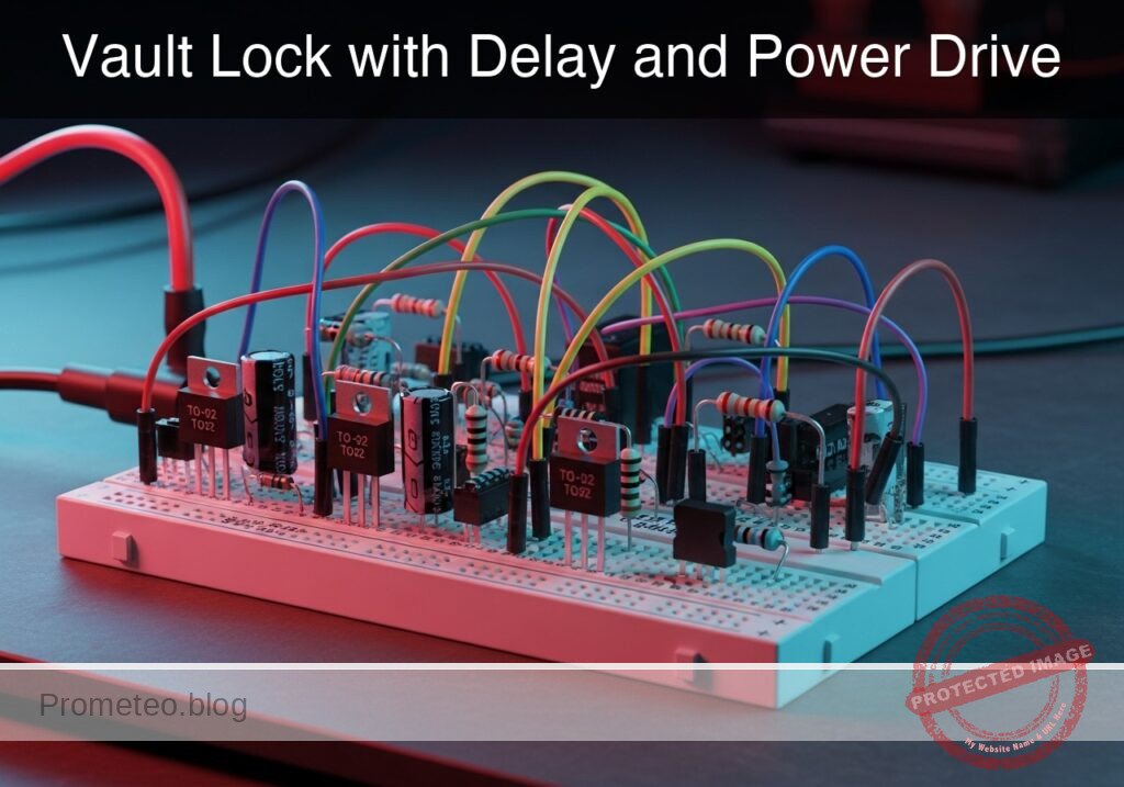
Level: Basic. Build a secure electronic lock that keeps a solenoid active for a few seconds after two keys are turned simultaneously.
Objective and use case
In this practical case, you will build a security circuit that requires two distinct inputs (keys/buttons) to be activated simultaneously to trigger a high-power mechanism. Once triggered, the system includes an analog memory (RC network) to hold the lock open for a short duration, allowing a user to open the door.
Real-world scenarios:
- Bank Vaults: Requires two bank managers to turn keys at the same time to prevent theft.
- Industrial Presses: Requires an operator to press buttons with both hands to ensure safety before the machine engages.
- Secure Entryways: Allows a door strike to remain unlatched for 5 seconds after authorization.
Expected outcome:
- Logic: The load (Solenoid/LED) remains OFF if only one button is pressed.
- Activation: The load turns ON fully only when both SW1 and SW2 are held.
- Timing: Upon releasing the buttons, the load remains ON for approximately 2 to 5 seconds before fading out.
- Target audience: Basic electronics students focusing on transistor switching and RC time constants.
Materials
- V1: 12 V DC supply, function: Main power source.
- SW1: Push button (Normally Open), function: Security Key 1.
- SW2: Push button (Normally Open), function: Security Key 2.
- R1: 1 kΩ resistor, function: Current limiter for capacitor charging (protection).
- R2: 47 kΩ resistor, function: Discharge timing resistor (Bleeder).
- C1: 100 µF electrolytic capacitor, function: Energy storage for time delay.
- Q1: IRF540 N-Channel MOSFET, function: Power switch for the load.
- L1: 10 mH inductor, function: Solenoid coil simulation.
- R3: 10 Ω resistor, function: Internal resistance of the solenoid.
- D1: 1N4007 Diode, function: Flyback protection against inductive voltage spikes.
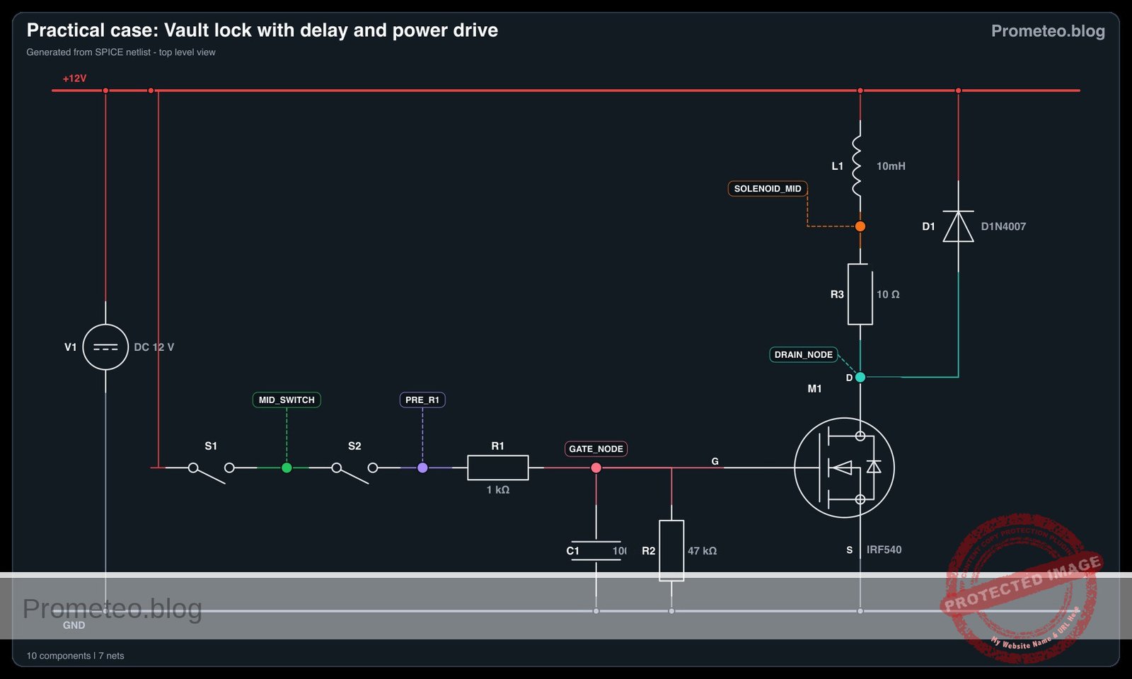
Wiring guide
This guide uses the node names 12 V, 0 (Ground), Mid_Switch, Gate_Node, and Drain_Node.
Logic Stage (Series AND):
- V1 (Positive) connects to SW1 (Input).
- SW1 (Output) connects to
Mid_Switch. - SW2 (Input) connects to
Mid_Switch. - SW2 (Output) connects to R1 (Input).
Timing Stage (RC Hold):
- R1 (Output) connects to
Gate_Node. - C1 (Positive) connects to
Gate_Node. - C1 (Negative) connects to
0. - R2 connects between
Gate_Nodeand0(Parallel to C1). - Q1 (Gate) connects to
Gate_Node.
- R1 (Output) connects to
Power Stage:
- Q1 (Source) connects to
0. - Q1 (Drain) connects to
Drain_Node. - L1 and R3 (representing the Solenoid) are connected in series between
12 VandDrain_Node. - D1 (Cathode) connects to
12 V. - D1 (Anode) connects to
Drain_Node(across the load).
- Q1 (Source) connects to
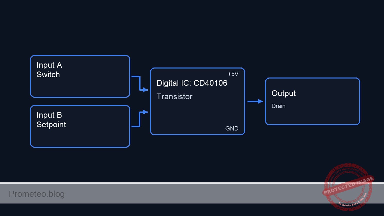
Conceptual block diagram
Schematic
Title: Practical case: Vault Lock with Delay and Power Drive

(1) LOGIC & TIMING STAGE
------------------------
                                                                    (Gate_Node)
[ 12 V ] --(Logic)--> [ SW1 ] --> [ SW2 ] --> [ R1: 1k ] --+------------+----------> [ Q1:Gate ]
                                                          |            |                |
                                                          |            |                |
                                                          v            v                |
                                                    [ C1: 100uF ]  [ R2: 47k ]          |
                                                          |            |                |
                                                          v            v                |
                                                         GND          GND               |
                                                                                        |
(2) POWER DRIVE STAGE                                                                   |
---------------------                                                                   |
                                                                                        |
[ 12 V ] --(Power)-----------------------------------------+                             |
   |                                                      |                             |
   |                                                      v                             |
   |                                              [ Solenoid (L1+R3) ]                  |
   |                                                      |                             |
   |                                                      v                             |
   +----(Cathode)-- [ D1: Flyback ] --(Anode)----> (Drain_Node) ----> [ Q1:Drain ]      |
                                                                            |           |
                                                                            +-----------+
                                                                            |
                                                                      (Internal FET)
                                                                            |
                                                                            v
                                                                      [ Q1:Source ]
                                                                            |
                                                                            v
                                                                           GND
Electrical diagram
Measurements and tests
Validate the circuit operation using a multimeter or oscilloscope:
- Logic Verification: Press SW1 only. Measure voltage at
Gate_Node. It should be 0 V. Repeat for SW2 only. The load should remain OFF. - Activation: Press SW1 and SW2 simultaneously. Measure voltage at
Gate_Node. It should rise immediately to approx 12 V. The Solenoid (Load) should activate. - Hold Time (Delay): Release both buttons simultaneously. Watch the load.
- The voltage at
Gate_Nodewill begin to drop. - The Solenoid should remain active.
- Measure the time it takes for the load to turn off (typically when Gate voltage drops below the MOSFET Threshold, ~3-4 V). With 47 kΩ and 100µF, this should be roughly 3 to 5 seconds.
- The voltage at
- Flyback Check: (Oscilloscope only) Monitor
Drain_Nodewhen the transistor turns off. You should not see a massive voltage spike above 12 V, confirming D1 is clamping the inductive kickback.
SPICE netlist and simulation
Reference SPICE Netlist (ngspice) — excerptFull SPICE netlist (ngspice)
* Practical case: Vault Lock with Delay and Power Drive
.width out=256

* --- Models ---
* Generic Switch Model for Push Buttons
.model SW_push SW(Vt=2.5 Ron=0.01 Roff=100Meg)

* Power MOSFET Model (Approximation of IRF540)
* N-Channel, Threshold ~4V, Low Rds(on)
.model IRF540 NMOS(Level=1 Vto=4.0 Kp=20 Lambda=0.001 Rd=0.05 Rs=0.05)

* Diode Model (1N4007)
.model D1N4007 D(Is=14.11n N=1.984 Rs=33.89m Ikf=100m Cjo=20p M=0.3333 Vj=0.75 Bv=1000 Ibv=10u)

* --- Main Power Supply ---
V1 12V 0 DC 12

* --- User Interface (Push Buttons) ---
* We simulate physical button presses using Pulse Voltage Sources controlling switches.
* Logic: To unlock, SW1 and SW2 must be pressed simultaneously (AND logic).
* ... (truncated in public view) ...
Copy this content into a .cir file and run with ngspice.
* Practical case: Vault Lock with Delay and Power Drive
.width out=256

* --- Models ---
* Generic Switch Model for Push Buttons
.model SW_push SW(Vt=2.5 Ron=0.01 Roff=100Meg)

* Power MOSFET Model (Approximation of IRF540)
* N-Channel, Threshold ~4V, Low Rds(on)
.model IRF540 NMOS(Level=1 Vto=4.0 Kp=20 Lambda=0.001 Rd=0.05 Rs=0.05)

* Diode Model (1N4007)
.model D1N4007 D(Is=14.11n N=1.984 Rs=33.89m Ikf=100m Cjo=20p M=0.3333 Vj=0.75 Bv=1000 Ibv=10u)

* --- Main Power Supply ---
V1 12V 0 DC 12

* --- User Interface (Push Buttons) ---
* We simulate physical button presses using Pulse Voltage Sources controlling switches.
* Logic: To unlock, SW1 and SW2 must be pressed simultaneously (AND logic).
V_act1 Ctrl1 0 PULSE(0 5 1 1m 1m 3 10)
V_act2 Ctrl2 0 PULSE(0 5 2.5 1m 1m 3 10)

* --- Logic Stage (Series AND) ---
* SW1 connects 12V to Mid_Switch
S1 12V Mid_Switch Ctrl1 0 SW_push

* SW2 connects Mid_Switch to R1 Input
S2 Mid_Switch Pre_R1 Ctrl2 0 SW_push

* --- Timing Stage (RC Hold) ---
* R1: Current limiter for charging
R1 Pre_R1 Gate_Node 1k

* C1: Energy storage (Timing capacitor)
C1 Gate_Node 0 100u

* R2: Discharge timing resistor (Bleeder)
* Time Constant (Discharge) = 47k * 100u = 4.7 seconds
R2 Gate_Node 0 47k

* --- Power Stage ---
* Q1 renamed to M1 to match SPICE MOSFET syntax (requires M prefix for NMOS model).
* Pin order: Drain Gate Source Bulk. Bulk connected to Source (0).
M1 Drain_Node Gate_Node 0 0 IRF540

* --- Load (Solenoid Simulation) ---
* Modeled as Inductor L1 and Resistor R3 in series
L1 12V Solenoid_Mid 10mH
R3 Solenoid_Mid Drain_Node 10

* --- Protection ---
* D1: Flyback diode to suppress inductive spikes from L1 upon turn-off
* Connected Cathode to 12V, Anode to Drain
D1 Drain_Node 12V D1N4007

* --- Simulation Commands ---
.op
* Transient analysis: 10ms step for 10 seconds to capture full charge/discharge cycle
.tran 10m 10s

* --- Output ---
* Monitoring Control signals, Gate voltage (Timing), and Drain voltage (Output state)
.print tran V(Ctrl1) V(Ctrl2) V(Gate_Node) V(Drain_Node) I(L1)

.end
Simulation Results (Transient Analysis)

Show raw data table (1095 rows)
Index   time            v(ctrl1)        v(ctrl2)        v(gate_node)    v(drain_node)   l1#branch
0	0.000000e+00	0.000000e+00	0.000000e+00	2.819323e-03	1.200000e+01	1.199844e-11
1	1.000000e-04	0.000000e+00	0.000000e+00	2.819323e-03	1.200000e+01	1.204503e-11
2	2.000000e-04	0.000000e+00	0.000000e+00	2.819323e-03	1.200000e+01	1.196043e-11
3	4.000000e-04	0.000000e+00	0.000000e+00	2.819323e-03	1.200000e+01	1.204260e-11
4	8.000000e-04	0.000000e+00	0.000000e+00	2.819323e-03	1.200000e+01	1.204346e-11
5	1.600000e-03	0.000000e+00	0.000000e+00	2.819323e-03	1.200000e+01	1.201220e-11
6	3.200000e-03	0.000000e+00	0.000000e+00	2.819323e-03	1.200000e+01	1.199165e-11
7	6.400000e-03	0.000000e+00	0.000000e+00	2.819323e-03	1.200000e+01	1.202979e-11
8	1.280000e-02	0.000000e+00	0.000000e+00	2.819323e-03	1.200000e+01	1.202182e-11
9	2.280000e-02	0.000000e+00	0.000000e+00	2.819323e-03	1.200000e+01	1.199840e-11
10	3.280000e-02	0.000000e+00	0.000000e+00	2.819323e-03	1.200000e+01	1.200551e-11
11	4.280000e-02	0.000000e+00	0.000000e+00	2.819323e-03	1.200000e+01	1.199929e-11
12	5.280000e-02	0.000000e+00	0.000000e+00	2.819323e-03	1.200000e+01	1.200551e-11
13	6.280000e-02	0.000000e+00	0.000000e+00	2.819323e-03	1.200000e+01	1.199929e-11
14	7.280000e-02	0.000000e+00	0.000000e+00	2.819323e-03	1.200000e+01	1.200551e-11
15	8.280000e-02	0.000000e+00	0.000000e+00	2.819323e-03	1.200000e+01	1.199929e-11
16	9.280000e-02	0.000000e+00	0.000000e+00	2.819323e-03	1.200000e+01	1.200551e-11
17	1.028000e-01	0.000000e+00	0.000000e+00	2.819323e-03	1.200000e+01	1.199929e-11
18	1.128000e-01	0.000000e+00	0.000000e+00	2.819323e-03	1.200000e+01	1.200551e-11
19	1.228000e-01	0.000000e+00	0.000000e+00	2.819323e-03	1.200000e+01	1.199929e-11
20	1.328000e-01	0.000000e+00	0.000000e+00	2.819323e-03	1.200000e+01	1.200551e-11
21	1.428000e-01	0.000000e+00	0.000000e+00	2.819323e-03	1.200000e+01	1.199929e-11
22	1.528000e-01	0.000000e+00	0.000000e+00	2.819323e-03	1.200000e+01	1.200551e-11
23	1.628000e-01	0.000000e+00	0.000000e+00	2.819323e-03	1.200000e+01	1.199929e-11
... (1071 more rows) ...
Common mistakes and how to avoid them
- Omitting the Flyback Diode (D1):
- Error: The MOSFET fails after a few cycles due to high voltage spikes from the solenoid.
- Solution: Always place a diode in parallel with inductive loads, cathode to positive supply.
- Wrong Capacitor Polarity:
- Error: C1 explodes or heats up; circuit acts as a short.
- Solution: Ensure the negative stripe of the electrolytic capacitor connects to Ground (
0).
- Gate Floating:
- Error: If R2 is removed, the lock stays stuck «ON» indefinitely because the gate charge has nowhere to go.
- Solution: Ensure R2 is connected between Gate and Ground to provide a discharge path.
Troubleshooting
- Solenoid turns off instantly (No delay):
- Cause: C1 is too small, damaged, or R2 is too low (e.g., 1 kΩ instead of 47 kΩ).
- Fix: Check R2 value or increase C1 capacitance.
- MOSFET gets very hot during the «OFF» transition:
- Cause: Slow discharge causes the MOSFET to linger in the «linear region» (acting as a resistor) for too long.
- Fix: This is expected in simple RC delay circuits. Ensure the MOSFET has a heatsink or switch to a Logic-based delay (Schmitt Trigger) for a sharper cutoff.
- Circuit never activates:
- Cause: SW1 and SW2 are not wired in series, or MOSFET pinout (G-D-S) is incorrect.
- Fix: Verify continuity through the switches to the Gate pin.
Possible improvements and extensions
- Schmitt Trigger Snap-Action: Insert a Schmitt Trigger inverter (like CD40106) between the RC network and the MOSFET. This creates a clean, digital ON/OFF transition, preventing the MOSFET from heating up during the discharge phase.
- Emergency Reset: Add a «Panic» switch (Normally Closed) in parallel with the capacitor C1. Pressing it instantly shorts the capacitor, locking the vault immediately regardless of the remaining time.
More Practical Cases on Prometeo.blog
Find this product and/or books on this topic on Amazon
As an Amazon Associate, I earn from qualifying purchases. If you buy through this link, you help keep this project running.
Quick Quiz

Telecommunications Electronics Engineer and Computer Engineer (official degrees in Spain).

