Level: Medium. Design and verify a voltage stabilizer circuit using a Zener diode under load variations.
Objective and use case
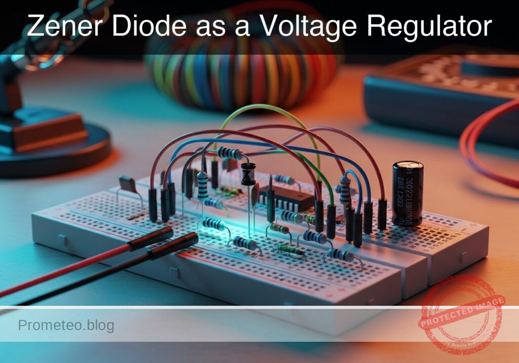
In this session, you will build a shunt voltage regulator using a Zener diode and a series limiting resistor to maintain a fixed 5.1 V output from a 9 V source.
- Why it is useful:
- Provides a stable reference voltage for Analog-to-Digital Converters (ADCs).
- Protects sensitive downstream components (like microcontrollers) from over-voltage spikes.
- Regulates voltage for low-power circuits without the complexity of an IC regulator.
- Expected outcome:
- The output voltage (VOUT) remains clamped at approximately 5.1 V despite the input being 9 V.
- Connecting a moderate load (470 Ω) decreases Zener current but maintains VOUT at 5.1 V.
- If the load resistance becomes too low, the regulation fails, and VOUT drops below 5.1 V.
- Target audience: Electronics students, Level: Medium.
Materials
- V1: 9 V DC voltage source, function: main power supply.
- R1: 220 Ω resistor, function: series current limiting (RS).
- D1: 1N4733 A Zener diode (5.1 V, 1 W), function: shunt voltage regulator.
- R2: 470 Ω resistor, function: load simulation (RL).
- M1: Multimeter (Voltmeter mode), function: measure output voltage.
- M2: Multimeter (Ammeter mode), function: measure Zener current (IZ).
Wiring guide
Construct the circuit using the following connections and SPICE node names (VIN, VOUT, 0):
- V1 (9 V Supply): Connect Positive terminal to node
VINand Negative terminal to node0(GND). - R1 (Series Resistor): Connect one terminal to
VINand the other terminal to nodeVOUT. - D1 (Zener Diode): Connect the Cathode (striped end) to node
VOUTand the Anode to node0. - R2 (Load Resistor): Connect one terminal to
VOUTand the other terminal to node0. - Measurements:
- To measure VOUT: Connect the Voltmeter Positive probe to
VOUTand Negative probe to0. - To measure IZ: Break the connection between D1 Cathode and
VOUT, and insert the Ammeter in series (Positive toVOUT, Negative to D1 Cathode).
- To measure VOUT: Connect the Voltmeter Positive probe to
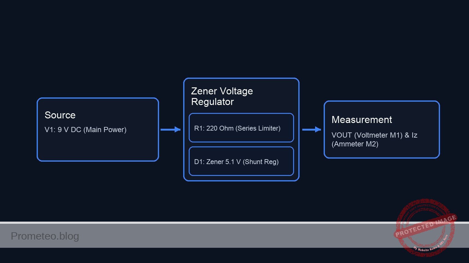
Conceptual block diagram

Schematic
[ SOURCE ]                 [ LIMITING ]                     [ REGULATION, LOAD & MEASUREMENT ]

                                                                           (Branch 1: Regulation)
                                                                 +---> [ Ammeter M2 ] --> [ D1: Zener 5.1 V ] --> GND
                                                                 |     (Measure Iz)       (Shunt Regulator)
                                                                 |
    [ V1: 9 V DC ] --(VIN)--> [ R1: 220 Ohm ] --(Node VOUT)--> ---+
    (Main Power)             (Series Resistor)                   |         (Branch 2: Load)
                                                                 +---> [ R2: 470 Ohm ] ------------------------> GND
                                                                 |     (Load Simulation)
                                                                 |
                                                                 |         (Branch 3: Monitoring)
                                                                 +---> [ Voltmeter M1 ] -----------------------> GND
                                                                       (Measure Vout)
Measurements and tests
Follow these steps to validate the regulator design:
-
Open Circuit Test (No Load):
- Temporarily disconnect R2.
- Measure voltage at
VOUT. It should read approximately 5.1 V. - Calculate the current flowing through the Zener: IZ = (VIN – VZ) / R1. Expect ≈ 17.7 mA.
-
Load Regulation Test:
- Reconnect R2 (470 Ω) between
VOUTand0. - Measure
VOUTagain. It should remain stable at 5.1 V. - Observe the Zener current. It should decrease because some current is now diverted through the load RL.
- Expected Load Current (IL): 5.1 V / 470 Ω ≈ 10.8 mA.
- Remaining Zener Current: ≈ 17.7 mA – 10.8 mA = 6.9 mA. Since IZ > 0, regulation holds.
- Reconnect R2 (470 Ω) between
-
Overload Test (Simulation):
- Replace R2 with a 100 Ω resistor (if available) or simulate a short.
- Measure
VOUT. The voltage will drop significantly below 5.1 V because the load demands more current than R1 can supply while maintaining the Zener breakdown voltage.
SPICE netlist and simulation
Reference SPICE Netlist (ngspice) — excerptFull SPICE netlist (ngspice)
* Practical case: Zener Diode as a Voltage Regulator

* --- Power Supply ---
* V1: 9 V DC voltage source (Main Supply)
V1 VIN 0 DC 9

* --- Components ---
* R1: 220 Ohm Resistor (Series Current Limiting)
* Wiring: Connect one terminal to VIN and the other to VOUT
R1 VIN VOUT 220

* R2: 470 Ohm Resistor (Load Simulation)
* Wiring: Connect one terminal to VOUT and the other to 0 (GND)
R2 VOUT 0 470

* M1: Multimeter (Voltmeter mode)
* Wiring: Positive probe to VOUT, Negative probe to 0
* Implementation: High impedance resistor to simulate voltmeter load
R_M1_Voltmeter VOUT 0 10Meg

* ... (truncated in public view) ...
Copy this content into a .cir file and run with ngspice.
* Practical case: Zener Diode as a Voltage Regulator

* --- Power Supply ---
* V1: 9 V DC voltage source (Main Supply)
V1 VIN 0 DC 9

* --- Components ---
* R1: 220 Ohm Resistor (Series Current Limiting)
* Wiring: Connect one terminal to VIN and the other to VOUT
R1 VIN VOUT 220

* R2: 470 Ohm Resistor (Load Simulation)
* Wiring: Connect one terminal to VOUT and the other to 0 (GND)
R2 VOUT 0 470

* M1: Multimeter (Voltmeter mode)
* Wiring: Positive probe to VOUT, Negative probe to 0
* Implementation: High impedance resistor to simulate voltmeter load
R_M1_Voltmeter VOUT 0 10Meg

* M2: Multimeter (Ammeter mode)
* Wiring: Inserted in series between VOUT and D1 Cathode
* Positive to VOUT, Negative to D1 Cathode (Node: VZ_CATHODE)
* Implementation: 0V DC source to measure current
V_M2_Ammeter VOUT VZ_CATHODE DC 0

* D1: 1N4733A Zener Diode (5.1 V, 1 W)
* Wiring: Cathode to VZ_CATHODE, Anode to 0
* Note: Cathode is connected to VOUT through the Ammeter
D1 0 VZ_CATHODE D1N4733A

* --- Models ---
* Model for 1N4733A Zener Diode
* BV=5.1V (Breakdown Voltage), IBV=49mA (Test Current)
.model D1N4733A D(IS=2.5n RS=1 N=1.2 BV=5.1 IBV=49m)

* --- Analysis ---
* Transient analysis (1ms simulation time)
.tran 1u 1ms

* --- Output Directives ---
* Print voltages and Zener current (Iz)
.print tran V(VIN) V(VOUT) I(V_M2_Ammeter)

* Operating Point for initial check
.op

.end
Simulation Results (Transient Analysis)
Show raw data table (1008 rows)
Index   time            v(vin)          v(vout)         v_m2_ammeter#br
0	0.000000e+00	9.000000e+00	5.047821e+00	7.223902e-03
1	1.000000e-08	9.000000e+00	5.047805e+00	7.224007e-03
2	2.000000e-08	9.000000e+00	5.047805e+00	7.224007e-03
3	4.000000e-08	9.000000e+00	5.047805e+00	7.224007e-03
4	8.000000e-08	9.000000e+00	5.047805e+00	7.224007e-03
5	1.600000e-07	9.000000e+00	5.047805e+00	7.224007e-03
6	3.200000e-07	9.000000e+00	5.047805e+00	7.224007e-03
7	6.400000e-07	9.000000e+00	5.047805e+00	7.224007e-03
8	1.280000e-06	9.000000e+00	5.047805e+00	7.224007e-03
9	2.280000e-06	9.000000e+00	5.047805e+00	7.224007e-03
10	3.280000e-06	9.000000e+00	5.047805e+00	7.224007e-03
11	4.280000e-06	9.000000e+00	5.047805e+00	7.224007e-03
12	5.280000e-06	9.000000e+00	5.047805e+00	7.224007e-03
13	6.280000e-06	9.000000e+00	5.047805e+00	7.224007e-03
14	7.280000e-06	9.000000e+00	5.047805e+00	7.224007e-03
15	8.280000e-06	9.000000e+00	5.047805e+00	7.224007e-03
16	9.280000e-06	9.000000e+00	5.047805e+00	7.224007e-03
17	1.028000e-05	9.000000e+00	5.047805e+00	7.224007e-03
18	1.128000e-05	9.000000e+00	5.047805e+00	7.224007e-03
19	1.228000e-05	9.000000e+00	5.047805e+00	7.224007e-03
20	1.328000e-05	9.000000e+00	5.047805e+00	7.224007e-03
21	1.428000e-05	9.000000e+00	5.047805e+00	7.224007e-03
22	1.528000e-05	9.000000e+00	5.047805e+00	7.224007e-03
23	1.628000e-05	9.000000e+00	5.047805e+00	7.224007e-03
... (984 more rows) ...
Common mistakes and how to avoid them
- Reversing the Zener Diode:
- Error: Connecting the Anode to
VOUTand Cathode to GND. - Result: The circuit behaves like a standard diode, clamping the output to ≈ 0.7 V instead of 5.1 V.
- Solution: Ensure the striped end (Cathode) is connected to the positive potential (
VOUT).
- Error: Connecting the Anode to
- Using a Series Resistor (R1) with too high resistance:
- Error: Using 10 kΩ instead of 220 Ω for R1.
- Result: When the load (R2) is connected, the voltage drops immediately; the Zener turns off because there isn’t enough current to keep it in breakdown.
- Solution: Calculate R1 such that enough current flows to satisfy both the load and the minimum Zener bias current (IZK).
- Exceeding Zener Power Rating:
- Error: Removing the load while using a very small R1.
- Result: All current flows through the Zener, causing it to overheat and potentially burn out.
- Solution: Ensure PZ = VZ × Izmax is less than the diode’s power rating (e.g., 1 W).
Troubleshooting
- Symptom: Output voltage is equal to Input voltage (9 V).
- Cause: Zener diode is open (broken) or not connected.
- Fix: Check connections to D1 or replace the diode.
- Symptom: Output voltage is ≈ 0.7 V.
- Cause: Zener diode is connected in forward bias (backwards).
- Fix: Reverse the diode orientation.
- Symptom: Output is 5.1 V without load, but drops to 3 V (or lower) when load is attached.
- Cause: The load resistance is too low (drawing too much current) or R1 is too high.
- Fix: Increase the load resistance or recalculate R1 for higher current delivery (watching power limits).
Possible improvements and extensions
- Series Pass Transistor: Add an NPN transistor (like a 2N2222) with the Zener controlling the base. This creates a Series Voltage Regulator capable of handling much higher load currents.
- Filtering: Add a capacitor (e.g., 10 µF) in parallel with the Zener diode to filter out noise and improve the stability of the voltage reference.
More Practical Cases on Prometeo.blog
Find this product and/or books on this topic on Amazon
As an Amazon Associate, I earn from qualifying purchases. If you buy through this link, you help keep this project running.


