Level: Medium
Design a circuit that decreases LED backlight intensity as ambient light increases.
Objective and use case
In this practical case, you will build a PWM (Pulse Width Modulation) controller using a 555 timer and a photoresistor (LDR). The circuit will automatically adjust the duty cycle of the output signal based on ambient light levels, driving a power MOSFET to dim an LED strip.
Why it is useful:
* Energy Efficiency: Reduces power consumption in high-brightness environments where backlights might be less visible or needed (depending on display type).
* Automatic Night-Lights: Useful for systems that need to be dim during the day and bright at night (if logic is inverted) or vice-versa.
* Human Vision Comfort: Prevents glare by adjusting light intensity dynamically.
* Instrumentation: Often used in automotive dashboards or control panels.
Expected outcome:
* Signal Generation: A square wave output at pin 3 of the 555 timer.
* Inverse Response: When the LDR is exposed to strong light (Flashlight), the LED brightness decreases.
* Dark Response: When the LDR is covered (Darkness), the LED brightness increases to maximum.
* Target Audience: Intermediate electronics students and hobbyists.
Materials
- V1: 9 V DC voltage source, function: Main circuit power.
- R1: Photoresistor (LDR), function: Light sensor (Charge path).
- R2: 10 kΩ resistor, function: Discharge path timing.
- R3: 1 kΩ resistor, function: MOSFET Gate protection.
- R4: 330 Ω resistor, function: LED current limiting.
- C1: 100 nF capacitor, function: PWM timing capacitor.
- C2: 10 nF capacitor, function: Control voltage noise filtering.
- D1: 1N4148 diode, function: Steering diode for Charge path.
- D2: 1N4148 diode, function: Steering diode for Discharge path.
- D3: High-brightness White LED, function: Simulated Backlight.
- Q1: 2N7000 (N-Channel MOSFET), function: LED driver switch.
- U1: NE555 Precision Timer, function: PWM generator.
Wiring guide
This guide uses specific node names (VCC, 0, V_TRIG, V_GATE, etc.) to help you verify connections.
- Power Supply:
- Connect V1 positive terminal to node
VCC. - Connect V1 negative terminal to node
0(GND). - 555 Timer Power & Reset (U1):
- Connect U1 pin 8 (VCC) to node
VCC. - Connect U1 pin 1 (GND) to node
0. - Connect U1 pin 4 (Reset) to node
VCC. - Timing Network (The PWM Core):
- Connect R1 (LDR) between node
VCCand nodeV_CHARGE. - Connect D1 (Anode) to
V_CHARGEand D1 (Cathode) to nodeV_TIMING. - Connect D2 (Anode) to node
V_TIMINGand D2 (Cathode) to nodeV_DISCHARGE. - Connect R2 between node
V_DISCHARGEand U1 pin 7 (Discharge). - Connect C1 between node
V_TIMINGand node0. - Connect U1 pin 2 (Trigger) to node
V_TIMING. - Connect U1 pin 6 (Threshold) to node
V_TIMING. - Control Voltage:
- Connect C2 between U1 pin 5 (CV) and node
0. - Output Stage:
- Connect R3 between U1 pin 3 (Output) and node
V_GATE. - Connect Q1 Gate to node
V_GATE. - Connect Q1 Source to node
0. - Connect Q1 Drain to node
V_LED_CATHODE. - Load (Backlight):
- Connect R4 between node
VCCand nodeV_LED_ANODE. - Connect D3 Anode to node
V_LED_ANODE. - Connect D3 Cathode to node
V_LED_CATHODE.
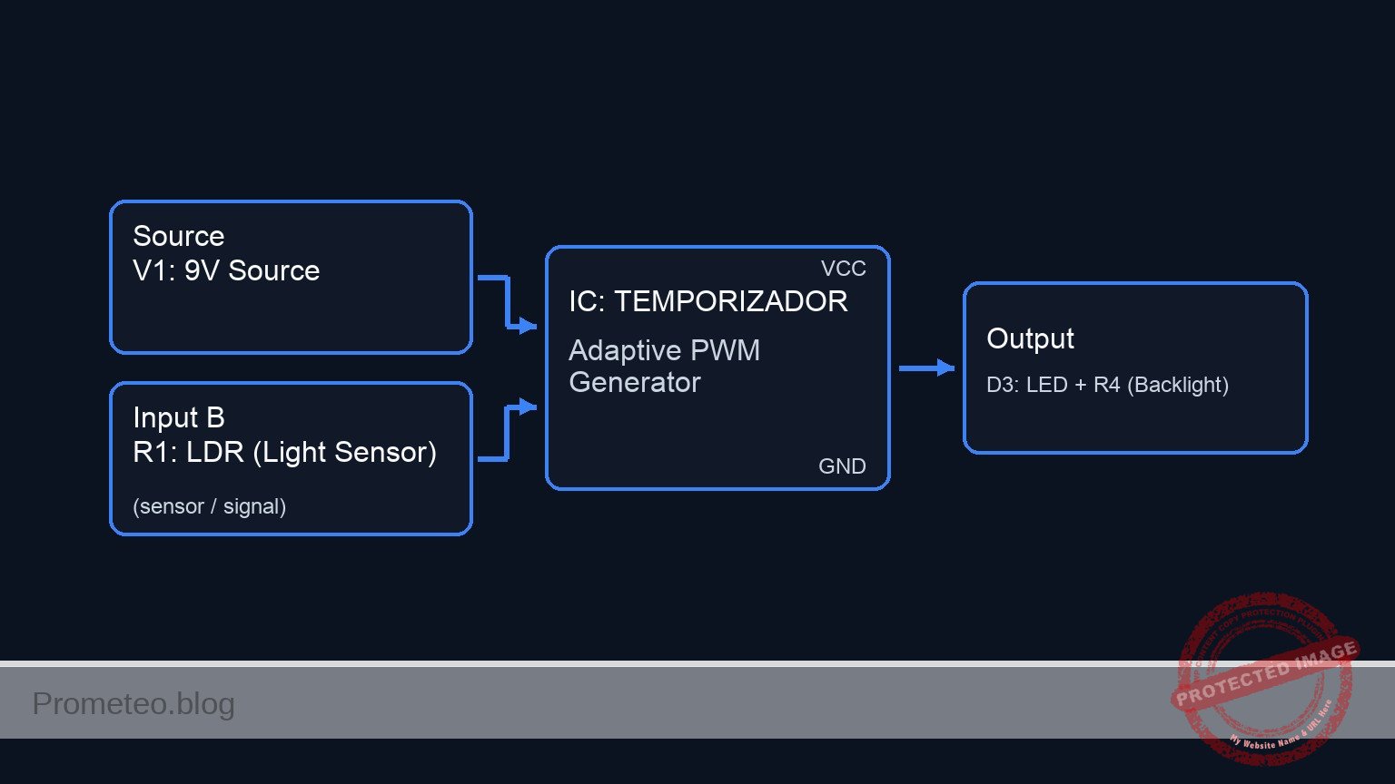
Conceptual block diagram
Schematic
Title: Practical case: Adaptive Screen Brightness Regulator

      [ INPUTS / TIMING NETWORK ]              [ LOGIC / CONTROL ]                 [ OUTPUT STAGE ]

[ V1: 9 V Source ] --(Power VCC)--------->+-----------------------+
                                         |                       |
(Light) -> [ R1: LDR ] --(Charge)------->|                       |
                                         |       U1: NE555       |
[ D1, D2, R2 ] --(Steering/Disch)------->|    (PWM Generator)    |--(Pin 3)--> [ R3: 1k ] --> [ Q1: MOSFET ]
                                         |                       |                                  |
[ C1: 100nF ] --(Timing Ramp)----------->|  Pins 2,6 (Trig/Thr)  |                                  |
                                         |  Pin 7 (Discharge)    |                           (Switches GND)
[ C2: 10nF ] --(Filter)----------------->|  Pin 5 (Ctrl Volt)    |                                  |
                                         |                       |                                  v
                                         +-----------------------+                       [ D3: LED + R4: 330R ]
                                                                                              (Backlight)
Measurements and tests
Perform these steps to validate the «Inverse» behavior (More light = Less Brightness).
- Baseline Check (Ambient Light):
- Power the circuit with 9 V.
- Observe the LED D3. It should be illuminated at a moderate level.
- Measure voltage at
V_GATEusing an oscilloscope. You should see a square wave.
- High Light Test:
- Shine a flashlight directly onto R1 (LDR).
- Observation: The LED D3 should dim significantly or turn off.
- Measurement: Check the duty cycle at
V_GATE. Since the LDR resistance drops, the capacitor charges very quickly (short Ton) relative to the fixed discharge time (Toff). The Duty Cycle (Ton / Ttotal) decreases.
- Low Light Test:
- Cover R1 (LDR) with your hand or a black cap.
- Observation: The LED D3 should reach maximum brightness.
- Measurement: The LDR resistance increases, making the charge time (Ton) much longer. The Duty Cycle increases towards 100%.
SPICE netlist and simulation
Reference SPICE Netlist (ngspice) — excerptFull SPICE netlist (ngspice)
* Practical case: Adaptive Screen Brightness Regulator

* --- Power Supply ---
V1 VCC 0 DC 9

* --- Input Stage (Light Sensor) ---
R1 VCC V_CHARGE 20k

* --- PWM Timing Network ---
D1 V_CHARGE V_TIMING D1N4148
D2 V_TIMING V_DISCHARGE D1N4148
R2 V_DISCHARGE V_DISCH_PIN 10k
C1 V_TIMING 0 100n

* --- Control & Processing ---
* U1: NE555 Precision Timer
XU1 0 V_TIMING V_OUT_PIN VCC V_CV V_TIMING V_DISCH_PIN VCC NE555

* Control Voltage noise filtering
C2 V_CV 0 10n
* ... (truncated in public view) ...
Copy this content into a .cir file and run with ngspice.
* Practical case: Adaptive Screen Brightness Regulator

* --- Power Supply ---
V1 VCC 0 DC 9

* --- Input Stage (Light Sensor) ---
R1 VCC V_CHARGE 20k

* --- PWM Timing Network ---
D1 V_CHARGE V_TIMING D1N4148
D2 V_TIMING V_DISCHARGE D1N4148
R2 V_DISCHARGE V_DISCH_PIN 10k
C1 V_TIMING 0 100n

* --- Control & Processing ---
* U1: NE555 Precision Timer
XU1 0 V_TIMING V_OUT_PIN VCC V_CV V_TIMING V_DISCH_PIN VCC NE555

* Control Voltage noise filtering
C2 V_CV 0 10n

* --- Output Driver Stage ---
R3 V_OUT_PIN V_GATE 1k

* Q1: N-Channel MOSFET
MQ1 V_LED_CATHODE V_GATE 0 0 2N7000

* --- Load (Backlight) ---
R4 VCC V_LED_ANODE 330
D3 V_LED_ANODE V_LED_CATHODE WHITE_LED

* --- Component Models ---
.model D1N4148 D (IS=2.682n N=1.836 RS=.5664 BV=100 IBV=100p CJO=4p TT=11.54n)
.model 2N7000 NMOS (Level=1 VTO=2.1 KP=0.5 Lambda=0.002 RD=1.5 RS=1.5 CGSO=10p CGDO=10p CGBO=10p)
.model WHITE_LED D (IS=1p N=5 RS=5 BV=5 IBV=10u CJO=50p)

* --- NE555 Behavioral Subcircuit ---
.subckt NE555 GND TRIG OUT RESET CV THRES DISCH VCC
    * Internal Voltage Divider
    R_div1 VCC CV 5k
    R_div2 CV TR 5k
    R_div3 TR GND 5k

    * Comparators (Sigmoid-based for smooth convergence)
    * Set Signal (Active High) when TRIG < 1/3 VCC (V_TR)
    B_set set_node 0 V = 2.5 + 2.5 * tanh(100 * (V(TR) - V(TRIG)))

    * Reset Signal Logic
    * Condition 1: THRES > CV
    B_c1 c1 0 V = 0.5 * (1 + tanh(100 * (V(THRES) - V(CV))))
    * Condition 2: RESET < 1.0V
    B_c2 c2 0 V = 0.5 * (1 + tanh(100 * (1.0 - V(RESET))))
    * Combine (Probabilistic OR logic): V_rst = c1 + c2 - c1*c2, scaled to 5V
    B_rst rst_node 0 V = 5 * (V(c1) + V(c2) - V(c1)*V(c2))

    * RC Delays to prevent algebraic loops in Flip-Flop
    R_sd set_node set_d 1k
    C_sd set_d 0 1p
    R_rd rst_node rst_d 1k
    C_rd rst_d 0 1p

    * SR Latch (Cross-coupled NOR logic with soft thresholds)
    * Q = ~(R | Qb)
    B_q  q_int  0 V = 5 / (1 + exp( 20 * (V(rst_d) + V(qb_int) - 2.5) ))
    * Qb = ~(S | Q)
    B_qb qb_int 0 V = 5 / (1 + exp( 20 * (V(set_d) + V(q_int) - 2.5) ))

    * Output Buffer
    E_out OUT_int 0 q_int 0 1
    R_out_prot OUT_int OUT 1

    * Discharge Transistor (Switch to GND when Qb is High / Output Low)
    S_disch DISCH 0 qb_int 0 SW_DISCH
    .model SW_DISCH SW(Vt=2.5 Ron=10 Roff=100Meg)
.ends

* --- Simulation Directives ---
.tran 10u 20m
.print tran V(V_TIMING) V(V_GATE) V(V_LED_CATHODE) V(V_LED_ANODE)
.op
.end
Simulation Results (Transient Analysis)

Show raw data table (4016 rows)
Index   time            v(v_timing)     v(v_gate)       v(v_led_cathode
0	0.000000e+00	3.183820e+00	9.643749e-22	8.709822e+00
1	1.000000e-07	3.183820e+00	9.643749e-22	8.709822e+00
2	2.000000e-07	3.183820e+00	-2.54330e-17	8.709822e+00
3	4.000000e-07	3.183820e+00	4.759196e-18	8.709822e+00
4	8.000000e-07	3.183820e+00	-5.90561e-18	8.709822e+00
5	1.600000e-06	3.183820e+00	1.843922e-17	8.709822e+00
6	3.200000e-06	3.183820e+00	4.911091e-18	8.709822e+00
7	6.400000e-06	3.183819e+00	9.652751e-18	8.709822e+00
8	1.280000e-05	3.183819e+00	-2.42211e-18	8.709822e+00
9	2.280000e-05	3.183818e+00	-2.25892e-17	8.709822e+00
10	3.280000e-05	3.183818e+00	-5.29878e-18	8.709822e+00
11	4.280000e-05	3.183817e+00	-8.38426e-18	8.709822e+00
12	5.280000e-05	3.183816e+00	-5.24090e-18	8.709822e+00
13	6.280000e-05	3.183815e+00	5.344924e-18	8.709822e+00
14	7.280000e-05	3.183815e+00	-6.20163e-18	8.709822e+00
15	8.280000e-05	3.183814e+00	-2.95146e-18	8.709822e+00
16	9.280000e-05	3.183813e+00	-1.95605e-17	8.709822e+00
17	1.028000e-04	3.183813e+00	5.833300e-18	8.709822e+00
18	1.128000e-04	3.183812e+00	-9.79628e-18	8.709822e+00
19	1.228000e-04	3.183812e+00	1.090495e-18	8.709822e+00
20	1.328000e-04	3.183811e+00	-1.79618e-17	8.709822e+00
21	1.428000e-04	3.183810e+00	6.632650e-18	8.709822e+00
22	1.528000e-04	3.183810e+00	-1.47697e-17	8.709822e+00
23	1.628000e-04	3.183809e+00	6.958764e-18	8.709822e+00
... (3992 more rows) ...
Common mistakes and how to avoid them
- Reversing Steering Diodes (D1, D2):
- Error: Placing D1 or D2 backwards prevents the capacitor from charging or discharging properly.
- Solution: Ensure the black band (cathode) of D1 points towards the capacitor and the black band of D2 points towards Pin 7.
- Connecting LDR to Pin 7 directly:
- Error: Connecting the LDR without the steering diodes creates a standard astable oscillator where frequency changes drastically, but duty cycle control is less distinct.
- Solution: Use the diode steering topology described to separate the Charge (LDR) and Discharge (R2) paths.
- MOSFET Pinout Confusion:
- Error: Swapping Drain and Source on the 2N7000.
- Solution: Verify the datasheet. For 2N7000 (TO-92), looking at the flat side, pins are usually Source, Gate, Drain (left to right).
Troubleshooting
- Symptom: LED is always ON and does not change with light.
- Cause: MOSFET Gate floating or Pin 3 stuck High.
- Fix: Check R1 and C1 connections. Ensure Pin 2 and 6 are tied together.
- Symptom: LED is always OFF.
- Cause: LDR resistance is too low (short circuit) or LED connected backwards.
- Fix: Check LED polarity. Measure resistance of LDR in darkness; if it is 0 Ω, it is defective.
- Symptom: LED flickers visibly.
- Cause: Frequency is too low.
- Fix: Reduce the value of C1 (e.g., change from 100 nF to 10 nF) to increase the PWM frequency beyond human persistence of vision (> 100 Hz).
Possible improvements and extensions
- Minimum Brightness Clamp: Add a fixed resistor in series with the LDR (R1). This ensures that even in extremely bright light (low LDR resistance), there is still a minimum charge time, preventing the LED from turning off completely.
- Smoother Transition: Add a large capacitor across the LDR to filter out rapid changes in light (e.g., shadows from passing objects), creating a «fade» effect rather than an instant jump in brightness.
More Practical Cases on Prometeo.blog
Find this product and/or books on this topic on Amazon
As an Amazon Associate, I earn from qualifying purchases. If you buy through this link, you help keep this project running.
Quick Quiz

Telecommunications Electronics Engineer and Computer Engineer (official degrees in Spain).