
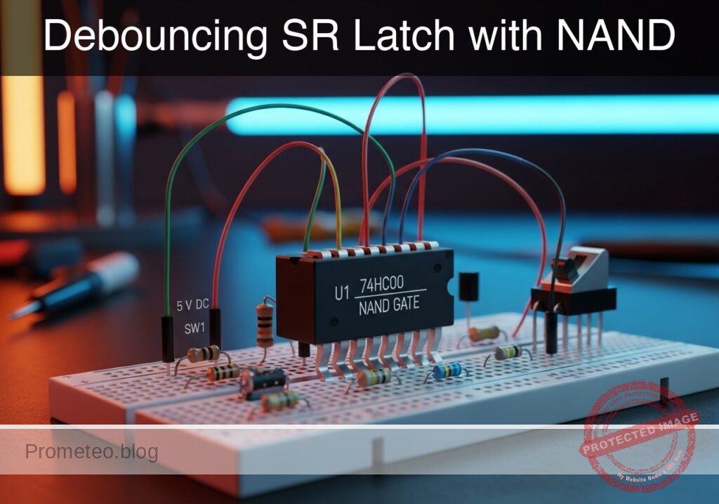
Level: Medium – Build a stable memory circuit to eliminate mechanical switch noise using cross-coupled NAND gates.
Objective and use case
In this practical case, you will build a Set-Reset (SR) Latch using a 74HC00 IC. By arranging two NAND gates in a cross-coupled feedback topology, the circuit creates a bistable memory element that ignores the mechanical «bouncing» noise generated when a physical switch contacts are closed.
Why it is useful:
* Mechanical switch interfacing: Essential for reading buttons in digital systems without false triggering.
* Microcontroller interrupts: Provides a clean edge (rising/falling) to trigger hardware interrupts reliably.
* State retention: Maintains the last known state (Set or Reset) even after the input trigger is released (return to idle).
* Industrial control: Used in «Start/Stop» motor control circuits where stability is safety-critical.
Expected outcome:
* Q Output: Stays HIGH (5 V) when Set is triggered and remains HIGH until Reset is triggered.
* Q_bar Output: Always the inverse of Q (Logic LOW when Q is HIGH).
* Visual feedback: Two LEDs (Green and Red) indicating the stored state clearly.
* Noise immunity: The output transitions once cleanly, even if the switch contacts bounce multiple times in milliseconds.
Target audience and level: Electronics students and intermediate hobbyists.
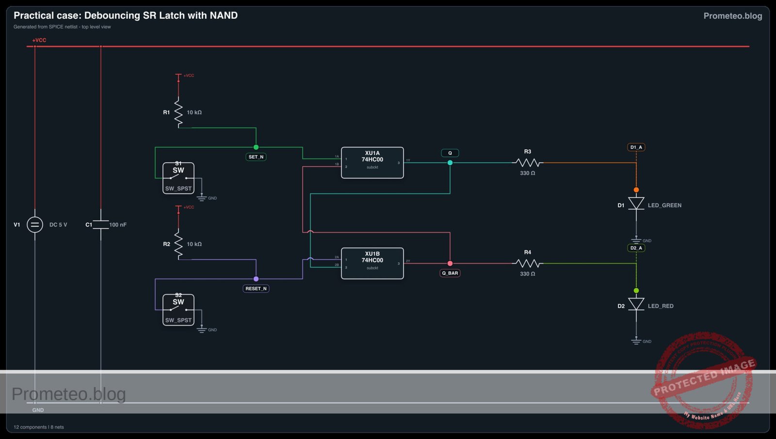
Materials
- V1: 5 V DC supply
- U1: 74HC00 (Quad 2-Input NAND Gate)
- SW1: SPDT (Single Pole Double Throw) switch, function: Set/Reset selector
- R1: 10 kΩ resistor, function: pull-up for SET_N
- R2: 10 kΩ resistor, function: pull-up for RESET_N
- R3: 330 Ω resistor, function: LED current limiting for Q
- R4: 330 Ω resistor, function: LED current limiting for Q_bar
- D1: Green LED, function: Indicator for State Q (Active)
- D2: Red LED, function: Indicator for State Q_bar (Inactive)
- C1: 100 nF capacitor, function: decoupling for U1 power pins
Pin-out of the IC used
Chip: 74HC00 (Quad 2-Input NAND Gate)
| Pin | Name | Logic function | Connection in this case |
|---|---|---|---|
| 1 | 1 A | Input | Connects to Node SET_N |
| 2 | 1B | Input | Connects to Node Q_BAR (Feedback) |
| 3 | 1Y | Output | Connects to Node Q |
| 4 | 2 A | Input | Connects to Node RESET_N |
| 5 | 2B | Input | Connects to Node Q (Feedback) |
| 6 | 2Y | Output | Connects to Node Q_BAR |
| 7 | GND | Ground | Connects to Node 0 |
| 14 | VCC | Power | Connects to Node VCC (5 V) |
Wiring guide
- Power Supply:
- Connect
V1positive terminal to nodeVCC. - Connect
V1negative terminal to node0(GND). - Connect
C1betweenVCCand0(close to U1). - Connect
U1pin 14 toVCC. Connect
U1pin 7 to0.Input Stage (Switch and Pull-ups):
- Connect
R1betweenVCCand nodeSET_N. - Connect
R2betweenVCCand nodeRESET_N. - Connect
SW1Common terminal to node0. - Connect
SW1Normally Open (NO) terminal to nodeSET_N. Connect
SW1Normally Closed (NC) terminal to nodeRESET_N. (Note: Toggling SW1 pulls one line Low while the other stays High).Logic Core (Cross-coupled NANDs):
- Connect
U1pin 1 (1 A) to nodeSET_N. - Connect
U1pin 2 (1B) to nodeQ_BAR. - Connect
U1pin 3 (1Y) to nodeQ. - Connect
U1pin 4 (2 A) to nodeRESET_N. - Connect
U1pin 5 (2B) to nodeQ. Connect
U1pin 6 (2Y) to nodeQ_BAR.Output Stage (Indicators):
- Connect
R3between nodeQandD1Anode. - Connect
D1Cathode to node0. - Connect
R4between nodeQ_BARandD2Anode. - Connect
D2Cathode to node0.
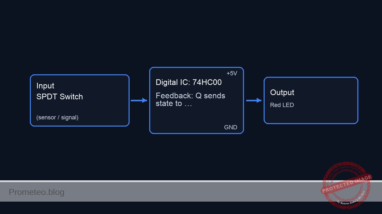
Conceptual block diagram
Schematic
Title: Practical case: Debouncing SR Latch with NAND

      INPUT STAGE (Switch & Pull-ups)           LOGIC CORE (74HC00 Latch)               OUTPUT STAGE (Indicators)
      ================================          =========================               =========================

      [ VCC ]
         |
         V
      [ R1: 10k Pull-up ]
         |
         V
      (Node: SET_N) --------------------------> [ U1: NAND Gate A ] --(Signal: Q)-----> [ R3: 330 ] --> [ D1: Green LED ] --> GND
         ^                                      ^       |
         |                                      |       |
      [ SW1: SPDT Switch ]                      |       +--(Feedback: Q sends state to Gate B)
      (Connects GND to SET_N or RESET_N)        |
         |                                      +--(Feedback: Q_BAR maintains state of Gate A)
         v                                              |
      (Node: RESET_N) ------------------------> [ U1: NAND Gate B ] --(Signal: Q_BAR)-> [ R4: 330 ] --> [ D2: Red LED ] ----> GND
         ^
         |
      [ R2: 10k Pull-up ]
         |
         ^
         |
      [ VCC ]


      POWER & DECOUPLING:
      [ VCC ] --(Power)--> [ U1: Pin 14 ]
      [ GND ] --(Ground)--> [ U1: Pin 7 ]
      [ VCC ] --(Filter)--> [ C1: 100nF ] --> [ GND ]
Electrical diagram
Truth table
The NAND SR Latch inputs are Active Low.
| SET_N (Input) | RESET_N (Input) | Q (Output) | Q_bar (Output) | State Description |
|---|---|---|---|---|
| 1 (High) | 1 (High) | Previous Q | Previous Q_bar | Hold (Memory) |
| 0 (Low) | 1 (High) | 1 | 0 | Set |
| 1 (High) | 0 (Low) | 0 | 1 | Reset |
| 0 (Low) | 0 (Low) | 1 | 1 | Invalid (Avoid) |
Measurements and tests
- Initial Power-Up: Turn on the 5 V supply. Ensure
SW1is in one specific position. - Verify Reset: Toggle
SW1to pullRESET_NLow (andSET_NHigh).- Confirm Red LED (
D2, Q_bar) turns ON. - Confirm Green LED (
D1, Q) turns OFF. - Measure voltage at
Q: should be approx 0 V.
- Confirm Red LED (
- Verify Set: Toggle
SW1to pullSET_NLow.- Confirm Green LED (
D1, Q) turns ON. - Confirm Red LED (
D2, Q_bar) turns OFF. - Measure voltage at
Q: should be approx 5 V.
- Confirm Green LED (
- Debounce Test: While moving the switch, observe the LEDs. They should switch states instantly without flickering, even if the switch contact is imperfect.
- Disconnect Test (Hold State): If you unplug the switch wires so both inputs are pulled High by R1/R2, the LEDs must maintain their last valid state.
SPICE netlist and simulation
Reference SPICE Netlist (ngspice) — excerptFull SPICE netlist (ngspice)
* Title: Practical case: Debouncing SR Latch with NAND
* NGSPICE Netlist
.width out=256

* --- Power Supply ---
V1 VCC 0 DC 5
C1 VCC 0 100n

* --- Input Stage (Switch and Pull-ups) ---
* R1 Pull-up for SET_N
R1 VCC SET_N 10k
* R2 Pull-up for RESET_N
R2 VCC RESET_N 10k

* --- Switch Simulation (SW1 SPDT) ---
* Control Signal Source
V_SW_CTRL CTRL 0 PULSE(0 5 100u 1u 1u 200u 600u)

* Inverted control signal for the NC contact
B_SW_INV CTRL_N 0 V=5-V(CTRL)
* ... (truncated in public view) ...
Copy this content into a .cir file and run with ngspice.
* Title: Practical case: Debouncing SR Latch with NAND
* NGSPICE Netlist
.width out=256

* --- Power Supply ---
V1 VCC 0 DC 5
C1 VCC 0 100n

* --- Input Stage (Switch and Pull-ups) ---
* R1 Pull-up for SET_N
R1 VCC SET_N 10k
* R2 Pull-up for RESET_N
R2 VCC RESET_N 10k

* --- Switch Simulation (SW1 SPDT) ---
* Control Signal Source
V_SW_CTRL CTRL 0 PULSE(0 5 100u 1u 1u 200u 600u)

* Inverted control signal for the NC contact
B_SW_INV CTRL_N 0 V=5-V(CTRL)

* Switch Models (Threshold 2.5V)
.model SW_MECH SW(Vt=2.5 Vh=0.1 Ron=0.1 Roff=100Meg)

* S1 (NO Contact): Connects SET_N to 0 when CTRL is High
S1 SET_N 0 CTRL 0 SW_MECH

* S2 (NC Contact): Connects RESET_N to 0 when CTRL_N is High (CTRL is Low)
S2 RESET_N 0 CTRL_N 0 SW_MECH

* --- Logic Core (74HC00 Quad 2-Input NAND) ---
* Subcircuit for 74HC00 using robust behavioral NAND gates
* Pinout: 1=1A, 2=1B, 3=1Y, 4=2A, 5=2B, 6=2Y, 7=GND, 14=VCC
.subckt 74HC00 1 2 3 4 5 6 7 14
    * Gate 1 (Pins 1, 2 -> Output 3)
    * Logic: NAND. Implementation: Sigmoid-based continuous function for convergence.
    * Vout = VCC * (1 - (Sigmoid(A) * Sigmoid(B)))
    B_NAND1 3 7 V=V(14) * (1 - ( (1/(1+exp(-50*(V(1)-2.5)))) * (1/(1+exp(-50*(V(2)-2.5)))) ))

    * Gate 2 (Pins 4, 5 -> Output 6)
    B_NAND2 6 7 V=V(14) * (1 - ( (1/(1+exp(-50*(V(4)-2.5)))) * (1/(1+exp(-50*(V(5)-2.5)))) ))
.ends

* --- Instantiate U1 ---
* Wiring per guide: 1=SET_N, 2=Q_BAR, 3=Q, 4=RESET_N, 5=Q, 6=Q_BAR, 7=0, 14=VCC
XU1 SET_N Q_BAR Q RESET_N Q Q_BAR 0 VCC 74HC00

* --- Output Stage (Indicators) ---
* R3 between node Q and D1 Anode
R3 Q D1_A 330
* D1 Green LED (Q Active)
D1 D1_A 0 LED_GREEN

* R4 between node Q_BAR and D2 Anode
R4 Q_BAR D2_A 330
* D2 Red LED (Q_BAR Inactive)
D2 D2_A 0 LED_RED

* LED Models
.model LED_GREEN D(Is=1e-22 Rs=5 N=1.5 Eg=2.1)
.model LED_RED D(Is=1e-22 Rs=5 N=1.5 Eg=1.8)

* --- Simulation Commands ---
.op
.tran 1u 1ms

* --- Measurements ---
* Listing SET_N (Input) and Q (Output) first
.print tran V(SET_N) V(Q) V(RESET_N) V(Q_BAR) V(CTRL)

.end
* --- GPT review (BOM/Wiring/SPICE) ---
* circuit_ok=true
* simulation_summary: The simulation confirms correct SR Latch behavior. At t=0, SET_N is Low and RESET_N is High, resulting in Q=High (Set state). At t=100us, the switch toggles: SET_N goes High and RESET_N goes Low, causing Q to go Low and Q_BAR to go High (Reset state). The latch holds state correctly between transitions.
* bom_vs_spice equivalences ignored:
*   - SW1 (SPDT Switch) is modeled using a voltage-controlled switch pair (S1, S2) driven by a PULSE source (V_SW_CTRL) and its inverse.
*   - U1 (74HC00 Quad NAND) is modeled using a behavioral subcircuit with sigmoid-based voltage sources.
* overall_comment: The circuit is a textbook example of a NAND-based SR latch used for switch debouncing. The SPICE implementation faithfully follows the wiring guide, using a clever behavioral model for the 74HC00 and a dual-switch setup to simulate the SPDT action. The transient analysis clearly demonstrates the Set and Reset actions corresponding to the switch position, matching the provided truth table perfectly.
* --------------------------------------
Simulation Results (Transient Analysis)

Show raw data table (1072 rows)
Index   time            v(set_n)        v(q)            v(reset_n)      v(q_bar)        v(ctrl)
0	0.000000e+00	4.999500e+00	3.709206e-68	4.999950e-05	5.000000e+00	0.000000e+00
1	1.000000e-08	4.999500e+00	3.709206e-68	4.999950e-05	5.000000e+00	0.000000e+00
2	2.000000e-08	4.999500e+00	3.709206e-68	4.999950e-05	5.000000e+00	0.000000e+00
3	4.000000e-08	4.999500e+00	3.709206e-68	4.999950e-05	5.000000e+00	0.000000e+00
4	8.000000e-08	4.999500e+00	3.709206e-68	4.999950e-05	5.000000e+00	0.000000e+00
5	1.600000e-07	4.999500e+00	3.709206e-68	4.999950e-05	5.000000e+00	0.000000e+00
6	3.200000e-07	4.999500e+00	3.709206e-68	4.999950e-05	5.000000e+00	0.000000e+00
7	6.400000e-07	4.999500e+00	3.709206e-68	4.999950e-05	5.000000e+00	0.000000e+00
8	1.280000e-06	4.999500e+00	3.709206e-68	4.999950e-05	5.000000e+00	0.000000e+00
9	2.280000e-06	4.999500e+00	3.709206e-68	4.999950e-05	5.000000e+00	0.000000e+00
10	3.280000e-06	4.999500e+00	3.709206e-68	4.999950e-05	5.000000e+00	0.000000e+00
11	4.280000e-06	4.999500e+00	3.709206e-68	4.999950e-05	5.000000e+00	0.000000e+00
12	5.280000e-06	4.999500e+00	3.709206e-68	4.999950e-05	5.000000e+00	0.000000e+00
13	6.280000e-06	4.999500e+00	3.709206e-68	4.999950e-05	5.000000e+00	0.000000e+00
14	7.280000e-06	4.999500e+00	3.709206e-68	4.999950e-05	5.000000e+00	0.000000e+00
15	8.280000e-06	4.999500e+00	3.709206e-68	4.999950e-05	5.000000e+00	0.000000e+00
16	9.280000e-06	4.999500e+00	3.709206e-68	4.999950e-05	5.000000e+00	0.000000e+00
17	1.028000e-05	4.999500e+00	3.709206e-68	4.999950e-05	5.000000e+00	0.000000e+00
18	1.128000e-05	4.999500e+00	3.709206e-68	4.999950e-05	5.000000e+00	0.000000e+00
19	1.228000e-05	4.999500e+00	3.709206e-68	4.999950e-05	5.000000e+00	0.000000e+00
20	1.328000e-05	4.999500e+00	3.709206e-68	4.999950e-05	5.000000e+00	0.000000e+00
21	1.428000e-05	4.999500e+00	3.709206e-68	4.999950e-05	5.000000e+00	0.000000e+00
22	1.528000e-05	4.999500e+00	3.709206e-68	4.999950e-05	5.000000e+00	0.000000e+00
23	1.628000e-05	4.999500e+00	3.709206e-68	4.999950e-05	5.000000e+00	0.000000e+00
... (1048 more rows) ...
Common mistakes and how to avoid them
- Leaving inputs floating: If you remove the switch and don’t have resistors R1/R2, the inputs float, causing unpredictable oscillation. Solution: Always use pull-up resistors (10 kΩ) on NAND latch inputs.
- Confusing Active Low vs. Active High: Users often expect «1» to set the latch. A NAND latch sets when the input goes to «0». Solution: Remember that NAND latches trigger on ground (Low) pulses.
- Forbidden State: pressing two buttons simultaneously (if using buttons instead of SPDT) creates Logic 0 on both inputs, forcing both outputs High. Solution: Mechanically prevent simultaneous presses or design logic to prioritize one input.
Troubleshooting
- Both LEDs are ON:
- Cause: Both
SET_NandRESET_Nare connected to Ground (Logic 0) simultaneously. - Fix: Check the switch wiring; ensure you are not shorting both inputs to ground.
- Cause: Both
- Circuit does not latch (LEDs flicker or follow switch loosely):
- Cause: Missing feedback connection.
- Fix: Ensure the wire from Pin 3 (
Q) goes to Pin 5, and Pin 6 (Q_BAR) goes to Pin 2.
- Chip gets hot:
- Cause: Output short circuit or reversed supply polarity.
- Fix: Check that R3 and R4 are present (do not connect LEDs directly to outputs) and verify Pin 14 is 5 V and Pin 7 is GND.
Possible improvements and extensions
- Gated SR Latch: Add two extra NAND gates (using the remaining two in the 74HC00) to add an «Enable» signal, turning it into a synchronous memory cell.
- Digital Counter Driver: Use the
Qoutput to drive the clock input of a CD4017 or 74HC4017 counter, proving that the manual button press generates exactly one clean clock pulse.
More Practical Cases on Prometeo.blog
Find this product and/or books on this topic on Amazon
As an Amazon Associate, I earn from qualifying purchases. If you buy through this link, you help keep this project running.
Quick Quiz

Telecommunications Electronics Engineer and Computer Engineer (official degrees in Spain).

