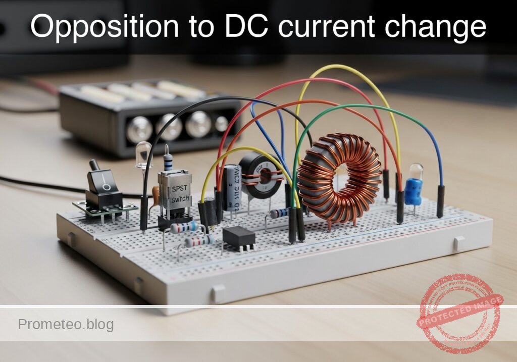
Level: Basic. Observe the delay in lamp activation due to self-induction.
Objective and use case
In this session, you will build a circuit that demonstrates how an inductor opposes rapid changes in current flow. By placing a large inductor in series with a lamp (with a parallel bypass resistor), you will create a visual «soft-start» effect where the light starts dim and gradually brightens.
Why it is useful:
* Inrush Current Limiting: Used in power supplies and large motors to prevent blown fuses when devices are first turned on.
* Soft-Start Circuits: Protects delicate filaments and components from thermal shock.
* Filtering: Smoothes out noise and ripples in DC power lines.
Expected outcome:
* When the switch is closed, the lamp will turn on immediately but dimly.
* Over a short period (0.5 to 2 seconds, depending on the inductance), the lamp will become fully bright.
* This visualizes the inductor initially acting as an «open circuit» (blocking current) and transitioning to a «short circuit» (allowing full flow).
* Target audience: Basic electronics students and hobbyists.
Materials
- V1: 12 V DC power supply or battery.
- S1: SPST mechanical switch (toggle or push-button).
- L1: 1 H to 2 H iron-core inductor, function: creates opposition to current change (e.g., a transformer primary winding used as a choke).
- R1: 220 Ω resistor (1 Watt or higher), function: bypass path for visual contrast.
- X1: 12 V / 100 mA incandescent lamp (small bulb), function: visual output load.
Wiring guide
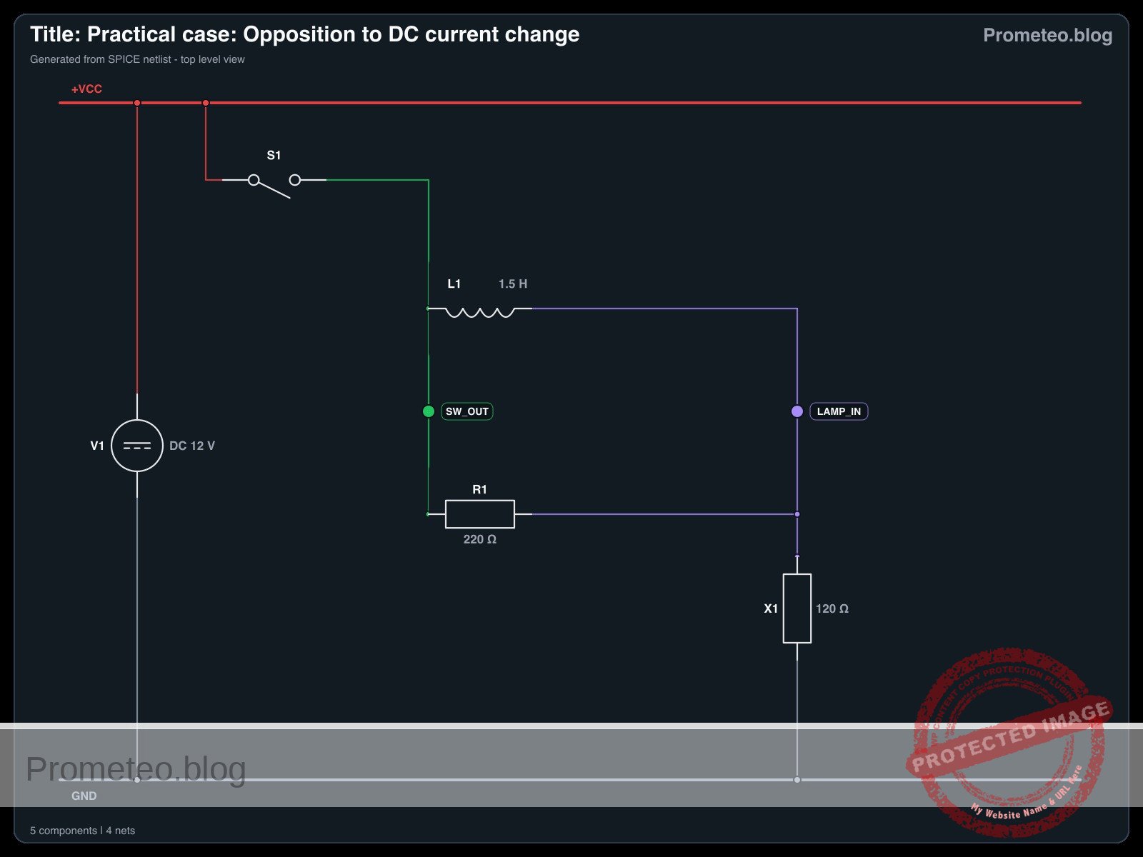
Construct the circuit using the following connections. The node names (e.g., VCC, SW_OUT) help identify the electrical points.
- V1 (DC Source): Connect the positive terminal to
VCCand the negative terminal to0(GND). - S1 (Switch): Connect between
VCCand nodeSW_OUT. - L1 (Inductor): Connect between node
SW_OUTand nodeLAMP_IN. - R1 (Resistor): Connect between node
SW_OUTand nodeLAMP_IN(this places R1 in parallel with L1). - X1 (Lamp): Connect between node
LAMP_INand0(GND).
Conceptual block diagram
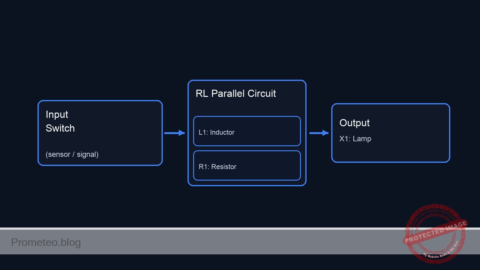
Schematic
(Node: SW_OUT)          (Node: LAMP_IN)
                                              /--> [ L1: Inductor ] --\
[ V1: 12 V Source ] --(VCC)--> [ S1: Switch ] --                        --> [ X1: Lamp ] --> GND
                                              \--> [ R1: Resistor ] --/
Electrical diagram
Measurements and tests
Follow these steps to validate the phenomenon:
- Initial State: Ensure the switch
S1is open. The lampX1should be off. - Observation: Keep your eyes on the lamp
X1. - Action: Close switch
S1. - Visual Validation:
- Phase 1 (Instant): The lamp lights up at roughly 30–50% brightness. (Current is flowing through
R1, asL1opposes the sudden change). - Phase 2 (Delay): The lamp brightness ramps up smoothly to 100%. (As the magnetic field in
L1stabilizes, it allows full current to pass, bypassingR1).
- Phase 1 (Instant): The lamp lights up at roughly 30–50% brightness. (Current is flowing through
- Voltage Measurement (Optional): If you have a multimeter, place probes across the Inductor (
SW_OUTtoLAMP_IN).- At the moment of contact, voltage is high (approx 6–8 V).
- After 1–2 seconds, voltage drops to near 0 V.
SPICE netlist and simulation
Reference SPICE Netlist (ngspice) — excerptFull SPICE netlist (ngspice)
* Title: Practical case: Opposition to DC current change
.width out=256
* Description: Demonstrates inductive opposition to current change (dim-to-bright lamp effect)

* --- Power Supply ---
* 12V DC Supply
V1 VCC 0 DC 12

* --- User Interface (Switch Control) ---
* Generates a control pulse to simulate pressing the button.
* Button Press: Starts at 10ms, Duration 300ms.
V_BTN_CTRL CTRL 0 PULSE(0 5 10m 1u 1u 300m 600m)

* --- Components ---

* S1: SPST Mechanical Switch
* Connected between VCC and SW_OUT.
* Modeled as a voltage-controlled switch driven by the control pulse.
S1 VCC SW_OUT CTRL 0 SW_IDEAL

* ... (truncated in public view) ...
Copy this content into a .cir file and run with ngspice.
* Title: Practical case: Opposition to DC current change
.width out=256
* Description: Demonstrates inductive opposition to current change (dim-to-bright lamp effect)

* --- Power Supply ---
* 12V DC Supply
V1 VCC 0 DC 12

* --- User Interface (Switch Control) ---
* Generates a control pulse to simulate pressing the button.
* Button Press: Starts at 10ms, Duration 300ms.
V_BTN_CTRL CTRL 0 PULSE(0 5 10m 1u 1u 300m 600m)

* --- Components ---

* S1: SPST Mechanical Switch
* Connected between VCC and SW_OUT.
* Modeled as a voltage-controlled switch driven by the control pulse.
S1 VCC SW_OUT CTRL 0 SW_IDEAL

* L1: 1.5H Iron-core Inductor
* Creates opposition to current change.
* Connected between SW_OUT and LAMP_IN.
L1 SW_OUT LAMP_IN 1.5

* R1: 220 Ohm Resistor
* Bypass path for visual contrast (parallel to L1).
* Connected between SW_OUT and LAMP_IN.
R1 SW_OUT LAMP_IN 220

* X1: 12V / 100mA Incandescent Lamp
* Modeled as a resistor: R = V / I = 12 / 0.1 = 120 Ohms.
* Connected between LAMP_IN and 0 (GND).
R_X1 LAMP_IN 0 120

* --- Models ---
* Ideal switch model: Low resistance when ON, High when OFF.
.model SW_IDEAL sw(vt=2.5 ron=0.01 roff=100Meg)

* --- Simulation Setup ---
* Transient analysis to capture the inductive time constant (approx 20ms).
* Simulation time: 500ms to allow full settling.
.op
.tran 1m 500m

* --- Output Directives ---
* V(SW_OUT): Input voltage to the LR network (Switch Output).
* V(LAMP_IN): Voltage across the Lamp (Visual Output).
.print tran V(SW_OUT) V(LAMP_IN) I(L1)

.end
Simulation Results (Transient Analysis)

Show raw data table (564 rows)
Index   time            v(sw_out)       v(lamp_in)      l1#branch
0	0.000000e+00	1.439998e-05	1.439998e-05	1.199999e-07
1	1.000000e-05	1.439998e-05	1.439998e-05	1.199999e-07
2	2.000000e-05	1.439998e-05	1.439998e-05	1.199999e-07
3	4.000000e-05	1.439998e-05	1.439998e-05	1.199999e-07
4	8.000000e-05	1.439998e-05	1.439998e-05	1.199999e-07
5	1.600000e-04	1.439998e-05	1.439998e-05	1.199999e-07
6	3.200000e-04	1.439998e-05	1.439998e-05	1.199999e-07
7	6.400000e-04	1.439998e-05	1.439998e-05	1.199999e-07
8	1.280000e-03	1.439998e-05	1.439998e-05	1.199999e-07
9	2.280000e-03	1.439998e-05	1.439998e-05	1.199999e-07
10	3.280000e-03	1.439998e-05	1.439998e-05	1.199999e-07
11	4.280000e-03	1.439998e-05	1.439998e-05	1.199999e-07
12	5.280000e-03	1.439998e-05	1.439998e-05	1.199999e-07
13	6.280000e-03	1.439998e-05	1.439998e-05	1.199999e-07
14	7.280000e-03	1.439998e-05	1.439998e-05	1.199999e-07
15	8.280000e-03	1.439998e-05	1.439998e-05	1.199999e-07
16	9.280000e-03	1.439998e-05	1.439998e-05	1.199999e-07
17	1.000000e-02	1.439998e-05	1.439998e-05	1.199999e-07
18	1.000010e-02	1.439998e-05	1.439998e-05	1.199999e-07
19	1.000026e-02	1.439998e-05	1.439998e-05	1.199999e-07
20	1.000031e-02	1.439998e-05	1.439998e-05	1.199999e-07
21	1.000039e-02	1.439998e-05	1.439998e-05	1.199999e-07
22	1.000041e-02	1.439998e-05	1.439998e-05	1.199999e-07
23	1.000045e-02	1.439998e-05	1.439998e-05	1.199999e-07
... (540 more rows) ...
Reference SPICE netlist (ngspice)
* Title: Practical case: Opposition to DC current change
.width out=256
* Description: Demonstrates inductive opposition to current change (dim-to-bright lamp effect)

* --- Power Supply ---
* 12V DC Supply
V1 VCC 0 DC 12

* --- User Interface (Switch Control) ---
* Generates a control pulse to simulate pressing the button.
* Button Press: Starts at 10ms, Duration 300ms.
V_BTN_CTRL CTRL 0 PULSE(0 5 10m 1u 1u 300m 600m)

* --- Components ---

* S1: SPST Mechanical Switch
* Connected between VCC and SW_OUT.
* Modeled as a voltage-controlled switch driven by the control pulse.
S1 VCC SW_OUT CTRL 0 SW_IDEAL

* L1: 1.5H Iron-core Inductor
* Creates opposition to current change.
* Connected between SW_OUT and LAMP_IN.
L1 SW_OUT LAMP_IN 1.5

* R1: 220 Ohm Resistor
* Bypass path for visual contrast (parallel to L1).
* Connected between SW_OUT and LAMP_IN.
R1 SW_OUT LAMP_IN 220

* X1: 12V / 100mA Incandescent Lamp
* Modeled as a resistor: R = V / I = 12 / 0.1 = 120 Ohms.
* Connected between LAMP_IN and 0 (GND).
R_X1 LAMP_IN 0 120

* --- Models ---
* Ideal switch model: Low resistance when ON, High when OFF.
.model SW_IDEAL sw(vt=2.5 ron=0.01 roff=100Meg)

* --- Simulation Setup ---
* Transient analysis to capture the inductive time constant (approx 20ms).
* Simulation time: 500ms to allow full settling.
.op
.tran 1m 500m

* --- Output Directives ---
* V(SW_OUT): Input voltage to the LR network (Switch Output).
* V(LAMP_IN): Voltage across the Lamp (Visual Output).
.print tran V(SW_OUT) V(LAMP_IN) I(L1)

.end
Simulation Results (Transient Analysis)
Common mistakes and how to avoid them
- Using an LED instead of an incandescent lamp: LEDs respond too quickly and have non-linear resistance, making the «ramp up» effect very hard to see. Solution: Always use an incandescent bulb or a coil-based relay for this demo.
- Inductor value too small: If you use a small air-core inductor (e.g., 100 µH), the delay will be microseconds, invisible to the eye. Solution: Use a large iron-core inductor, such as the primary coil of a mains transformer (ensure it is rated for the DC current).
- Omitting the parallel resistor: Without
R1, the lamp might simply stay off for a split second and then pop on, which can look like a switch bounce rather than a smooth transition. Solution:R1provides an immediate «dim» reference state, making the transition to «bright» much more obvious.
Troubleshooting
- Lamp lights fully bright instantly: The inductor value is too low, or the inductor is shorted. Check if you are using an air-core coil; switch to an iron-core one.
- Lamp never gets fully bright: The inductor might have a very high internal DC resistance (thin wire). Measure the resistance of the inductor coil; if it is comparable to the resistor
R1, the current will never fully bypass the resistor. - Sparks at the switch when turning off: Inductors generate back-EMF voltage when the circuit breaks.
R1acts as a snubber here, but if sparks persist, ensure your switch is rated for inductive loads.
Possible improvements and extensions
- Oscilloscope Visualization: Connect channel 1 of an oscilloscope across the Lamp. You will see an exponential curve rising, allowing you to calculate the Time Constant (\tau = L / R).
- Variable Delay: Replace
R1with a potentiometer and experiment with how changing the parallel resistance affects the initial «dim» brightness and the perceived transition speed.
More Practical Cases on Prometeo.blog
Find this product and/or books on this topic on Amazon
As an Amazon Associate, I earn from qualifying purchases. If you buy through this link, you help keep this project running.
Quick Quiz

Telecommunications Electronics Engineer and Computer Engineer (official degrees in Spain).