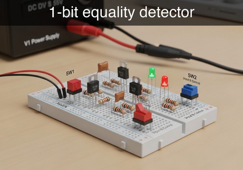
Level: Basic – Verify the operation of a 74HC7266 XNOR gate as a logical equality detector using its truth table.
Objective and use case
In this practical case, you will build a digital equality detector using a 74HC7266 XNOR logic gate, mechanical switches, and an LED indicator.
This circuit concept is highly useful in real-world digital electronics:
* Digital locks: Comparing an entered bit to a stored security key bit.
* Error detection: Verifying if two redundant sensor signals output the exact same digital state.
* Data routing: Confirming destination addresses in memory mapping or basic communication protocols.
* Automation: Checking if a machine’s actual state matches the commanded state.
Expected outcome:
* The output LED turns ON when both inputs are perfectly equal (both LOW or both HIGH).
* The output LED remains OFF when the inputs differ (one is HIGH and the other is LOW).
* Logic LOW is measured as approximately 0 V, and logic HIGH as approximately 5 V.
Target audience: Beginners learning fundamental digital logic gates and Boolean algebra.
Materials
- V1: 5 V DC power supply, function: circuit power
- SW1: SPST switch, function: input A control
- SW2: SPST switch, function: input B control
- R1: 10 kΩ resistor, function: pull-down for node VA
- R2: 10 kΩ resistor, function: pull-down for node VB
- R3: 330 Ω resistor, function: LED current limiting
- D1: red LED, function: equality indicator
- U1: 74HC7266 IC, function: XNOR logic gate
Pin-out of the 74HC7266
The 74HC7266 is a Quad 2-Input EXCLUSIVE-NOR (XNOR) gate with push-pull outputs.
| Pin | Name | Logic function | Connection in this case |
|---|---|---|---|
| 1 | 1 A | Input A of gate 1 | Node VA |
| 2 | 1B | Input B of gate 1 | Node VB |
| 3 | 1Y | Output of gate 1 | Node VOUT |
| 5, 6 | 2 A, 2B | Inputs of gate 2 | Node 0 (GND) |
| 7 | GND | Ground | Node 0 (GND) |
| 8, 9 | 3 A, 3B | Inputs of gate 3 | Node 0 (GND) |
| 12, 13 | 4 A, 4B | Inputs of gate 4 | Node 0 (GND) |
| 14 | VCC | Positive supply | Node VCC |
Note: Unused inputs (pins 5, 6, 8, 9, 12, 13) must be tied to ground to prevent CMOS oscillation and excess power draw.
Wiring guide
- V1: connects between node VCC and node 0 (GND).
- SW1: connects between node VCC and node VA.
- R1: connects between node VA and node 0.
- SW2: connects between node VCC and node VB.
- R2: connects between node VB and node 0.
- U1: VCC pin (14) connects to node VCC.
- U1: GND pin (7) connects to node 0.
- U1: Pin 1 (1 A) connects to node VA.
- U1: Pin 2 (1B) connects to node VB.
- U1: Pin 3 (1Y) connects to node VOUT.
- U1: Pins 5, 6, 8, 9, 12, and 13 connect directly to node 0.
- R3: connects between node VOUT and node D1_ANODE.
- D1: anode connects to node D1_ANODE, cathode connects to node 0.
Conceptual block diagram
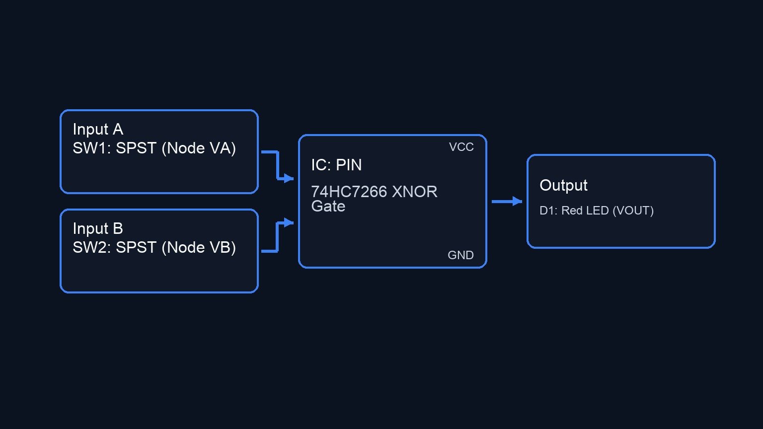
Schematic
VCC --> [ SW1: SPST ] --(Node VA)--> [ U1: Pin 1 (1 A) ]
                                            |
        (Node VA) --> [ R1: 10 kΩ ] --> GND  |
                                     [ U1: 74HC7266 XNOR ] --(Node VOUT)--> [ R3: 330 Ω ] --> [ D1: Red LED ] --> GND
        (Node VB) --> [ R2: 10 kΩ ] --> GND  |
                                            |
VCC --> [ SW2: SPST ] --(Node VB)--> [ U1: Pin 2 (1B) ]

* Power & Unused Pins:
  VCC --> [ U1: Pin 14 (VCC) ]
  GND <-- [ U1: Pin 7 (GND) ]
  GND <-- [ U1: Pins 5, 6, 8, 9, 12, 13 (Unused Inputs) ]
Electrical diagram
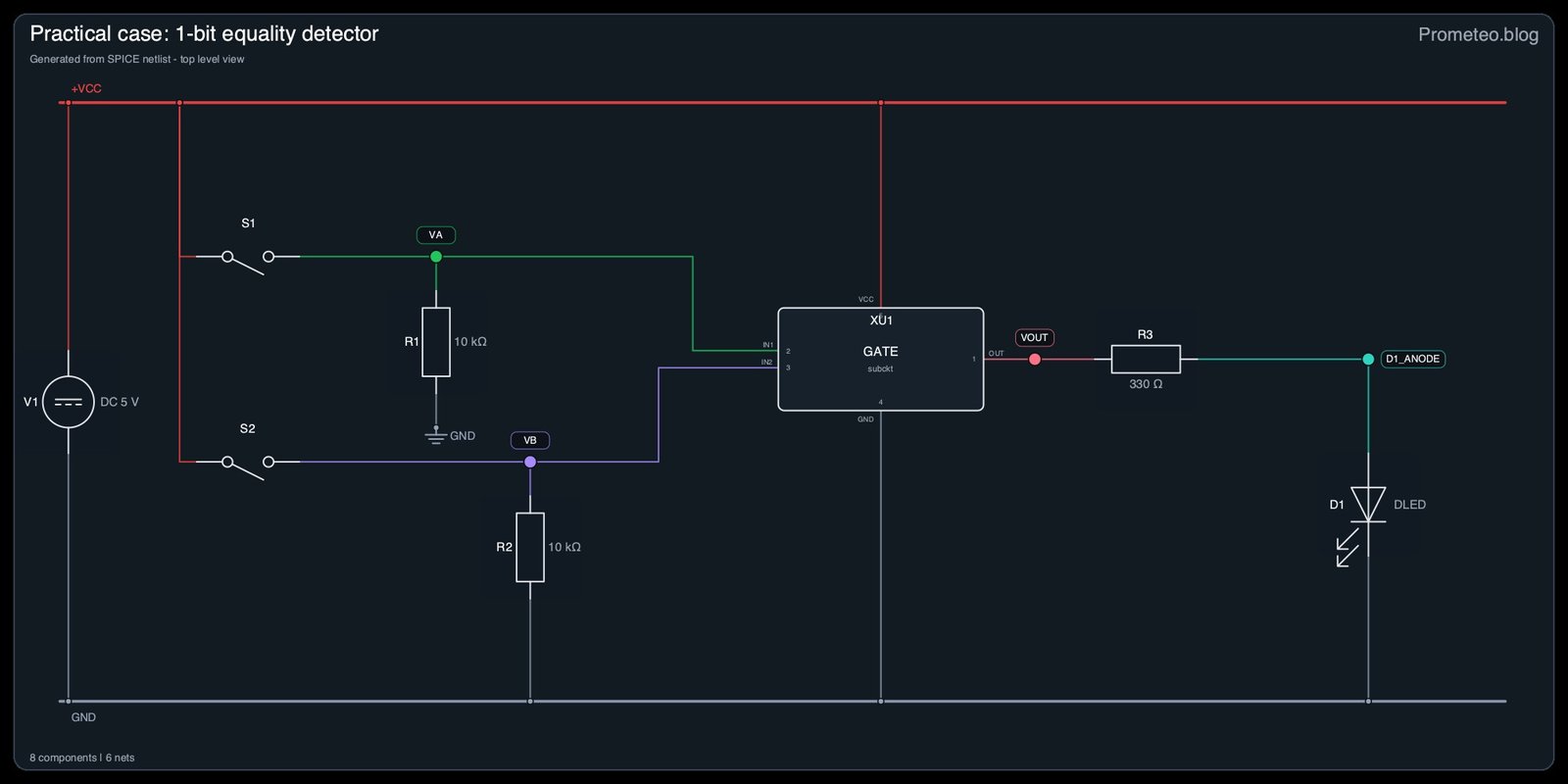
Truth table
| VA (Input A) | VB (Input B) | VOUT (Output) | D1 (LED Status) |
|---|---|---|---|
| 0 | 0 | 1 | ON |
| 0 | 1 | 0 | OFF |
| 1 | 0 | 0 | OFF |
| 1 | 1 | 1 | ON |
Measurements and tests
- Initial Power Verification: Before actuating any switches, power on the circuit. Measure the voltage between VCC and 0 to ensure it is 5 V.
- Input State Testing: Set your multimeter to DC Voltage. Measure nodes VA and VB with respect to node 0. Toggle SW1 and SW2 to verify that an open switch yields ~0 V (thanks to the pull-down resistors) and a closed switch yields ~5 V.
- XNOR Logic Verification: Measure the voltage at VOUT with respect to node 0 for all four combinations of SW1 and SW2.
- Equality Confirmation: Ensure VOUT is approximately 5 V and the LED is illuminated ONLY when VA and VB are perfectly matched (0 V & 0 V, or 5 V & 5 V).
SPICE netlist and simulation
Reference SPICE Netlist (ngspice) — excerptFull SPICE netlist (ngspice)
* Practical case: 1-bit equality detector
.width out=256

V1 VCC 0 DC 5

* Control signals for SW1 and SW2 to simulate user interaction
VctrlA ctrlA 0 PULSE(0 5 0 1u 1u 50u 100u)
VctrlB ctrlB 0 PULSE(0 5 0 1u 1u 100u 200u)

* SW1 and SW2 modeled as voltage-controlled switches
S1 VCC VA ctrlA 0 SWMOD
S2 VCC VB ctrlB 0 SWMOD

* Pull-down resistors R1 and R2
R1 VA 0 10k
R2 VB 0 10k

* U1: 74HC7266 XNOR Gate equivalent
XU1 VOUT VA VB 0 VCC GATE

* ... (truncated in public view) ...
Copy this content into a .cir file and run with ngspice.
* Practical case: 1-bit equality detector
.width out=256

V1 VCC 0 DC 5

* Control signals for SW1 and SW2 to simulate user interaction
VctrlA ctrlA 0 PULSE(0 5 0 1u 1u 50u 100u)
VctrlB ctrlB 0 PULSE(0 5 0 1u 1u 100u 200u)

* SW1 and SW2 modeled as voltage-controlled switches
S1 VCC VA ctrlA 0 SWMOD
S2 VCC VB ctrlB 0 SWMOD

* Pull-down resistors R1 and R2
R1 VA 0 10k
R2 VB 0 10k

* U1: 74HC7266 XNOR Gate equivalent
XU1 VOUT VA VB 0 VCC GATE

* LED current limiting resistor R3
R3 VOUT D1_ANODE 330

* Equality indicator LED D1
D1 D1_ANODE 0 DLED

* Subcircuit for canonical 2-input XNOR gate
.subckt GATE out in1 in2 gnd vcc
B1 out gnd V = 5 * (1 / (1 + exp(-5 * (V(in1)-2.5) * (V(in2)-2.5))))
.ends

* Models
.model SWMOD SW(VT=2.5 VH=0.2 RON=0.1 ROFF=100MEG)
.model DLED D(IS=1e-15 N=2.0 RS=10)

* Simulation commands
.op
.tran 1u 500u
.print tran V(VOUT) V(VA) V(VB) V(D1_ANODE)
.end
Simulation Results (Transient Analysis)

Show raw data table (694 rows)
Index   time            v(vout)         v(va)           v(vb)           v(d1_anode)
0	0.000000e+00	5.000000e+00	4.999500e-04	4.999500e-04	1.650722e+00
1	1.000000e-08	5.000000e+00	4.999500e-04	4.999500e-04	1.650721e+00
2	2.000000e-08	5.000000e+00	4.999500e-04	4.999500e-04	1.650721e+00
3	4.000000e-08	5.000000e+00	4.999500e-04	4.999500e-04	1.650721e+00
4	8.000000e-08	5.000000e+00	4.999500e-04	4.999500e-04	1.650721e+00
5	1.600000e-07	5.000000e+00	4.999500e-04	4.999500e-04	1.650721e+00
6	3.200000e-07	5.000000e+00	4.999500e-04	4.999500e-04	1.650721e+00
7	3.637500e-07	5.000000e+00	4.999500e-04	4.999500e-04	1.650721e+00
8	4.403125e-07	5.000000e+00	4.999500e-04	4.999500e-04	1.650721e+00
9	4.615039e-07	5.000000e+00	4.999500e-04	4.999500e-04	1.650721e+00
10	4.985889e-07	5.000000e+00	4.999500e-04	4.999500e-04	1.650721e+00
11	5.088535e-07	5.000000e+00	4.999500e-04	4.999500e-04	1.650721e+00
12	5.268165e-07	5.000000e+00	4.999500e-04	4.999500e-04	1.650721e+00
13	5.467041e-07	5.000000e+00	4.999950e+00	4.999950e+00	1.650721e+00
14	5.864794e-07	5.000000e+00	4.999950e+00	4.999950e+00	1.650721e+00
15	6.660299e-07	5.000000e+00	4.999950e+00	4.999950e+00	1.650721e+00
16	8.251311e-07	5.000000e+00	4.999950e+00	4.999950e+00	1.650721e+00
17	1.000000e-06	5.000000e+00	4.999950e+00	4.999950e+00	1.650721e+00
18	1.031820e-06	5.000000e+00	4.999950e+00	4.999950e+00	1.650721e+00
19	1.095461e-06	5.000000e+00	4.999950e+00	4.999950e+00	1.650721e+00
20	1.222742e-06	5.000000e+00	4.999950e+00	4.999950e+00	1.650721e+00
21	1.477303e-06	5.000000e+00	4.999950e+00	4.999950e+00	1.650721e+00
22	1.986427e-06	5.000000e+00	4.999950e+00	4.999950e+00	1.650721e+00
23	2.986427e-06	5.000000e+00	4.999950e+00	4.999950e+00	1.650721e+00
... (670 more rows) ...
Reference SPICE netlist (ngspice)
* Practical case: 1-bit equality detector
.width out=256

V1 VCC 0 DC 5

* Control signals for SW1 and SW2 to simulate user interaction
VctrlA ctrlA 0 PULSE(0 5 0 1u 1u 50u 100u)
VctrlB ctrlB 0 PULSE(0 5 0 1u 1u 100u 200u)

* SW1 and SW2 modeled as voltage-controlled switches
S1 VCC VA ctrlA 0 SWMOD
S2 VCC VB ctrlB 0 SWMOD

* Pull-down resistors R1 and R2
R1 VA 0 10k
R2 VB 0 10k

* U1: 74HC7266 XNOR Gate equivalent
XU1 VOUT VA VB 0 VCC GATE

* LED current limiting resistor R3
R3 VOUT D1_ANODE 330

* Equality indicator LED D1
D1 D1_ANODE 0 DLED

* Subcircuit for canonical 2-input XNOR gate
.subckt GATE out in1 in2 gnd vcc
B1 out gnd V = 5 * (1 / (1 + exp(-5 * (V(in1)-2.5) * (V(in2)-2.5))))
.ends

* Models
.model SWMOD SW(VT=2.5 VH=0.2 RON=0.1 ROFF=100MEG)
.model DLED D(IS=1e-15 N=2.0 RS=10)

* Simulation commands
.op
.tran 1u 500u
.print tran V(VOUT) V(VA) V(VB) V(D1_ANODE)
.end
Simulation Results (Transient Analysis)
Common mistakes and how to avoid them
- Confusing 74HC7266 with 74HC266: The 74HC266 has open-drain outputs, which means it cannot source current to turn on an LED without an external pull-up resistor. Ensure you use the 74HC7266 (push-pull) or add a pull-up resistor if using the 74HC266.
- Leaving CMOS inputs floating: Forgetting to ground the unused inputs of the 74HC7266 can cause internal high-frequency oscillation, drawing excessive current and potentially damaging the IC. Always tie unused inputs to GND or VCC.
- Omitting pull-down resistors: If R1 and R2 are forgotten, the inputs will float unpredictably when the switches are open, causing the LED to flicker randomly.
Troubleshooting
- Symptom: LED flickers or behaves erratically when switches are open.
- Cause: Node VA or VB is floating.
- Fix: Verify that R1 and R2 are securely connected between the switch inputs and ground.
- Symptom: LED never turns on.
- Cause: LED D1 is inserted backwards (reversed polarity) or R3 is too large (e.g., 100 kΩ instead of 330 Ω).
- Fix: Check the orientation of D1 (longer leg to D1_ANODE) and verify the value of R3.
- Symptom: LED is always ON regardless of switch positions.
- Cause: Output pin (3) is shorted to VCC, or both switches are permanently shorted to the same logic level.
- Fix: Inspect the wiring around VOUT, VA, and VB. Ensure the switches physically break the connection to VCC when toggled off.
Possible improvements and extensions
- Audible Equality Alert: Connect a 5 V active piezoelectric buzzer in parallel with the LED/resistor combination to provide an audible tone whenever the input bits match.
- 2-Bit Equality Detector: Use a second XNOR gate from the same IC for a second pair of inputs, and feed the outputs of both XNOR gates into an AND gate to verify if two 2-bit words are exactly equal.
More Practical Cases on Prometeo.blog
Find this product and/or books on this topic on Amazon
As an Amazon Associate, I earn from qualifying purchases. If you buy through this link, you help keep this project running.
Quick Quiz

Telecommunications Electronics Engineer and Computer Engineer (official degrees in Spain).