Level: Medium – Configure a capacitor in an NE555 circuit to control the oscillation frequency.
Objective and use case
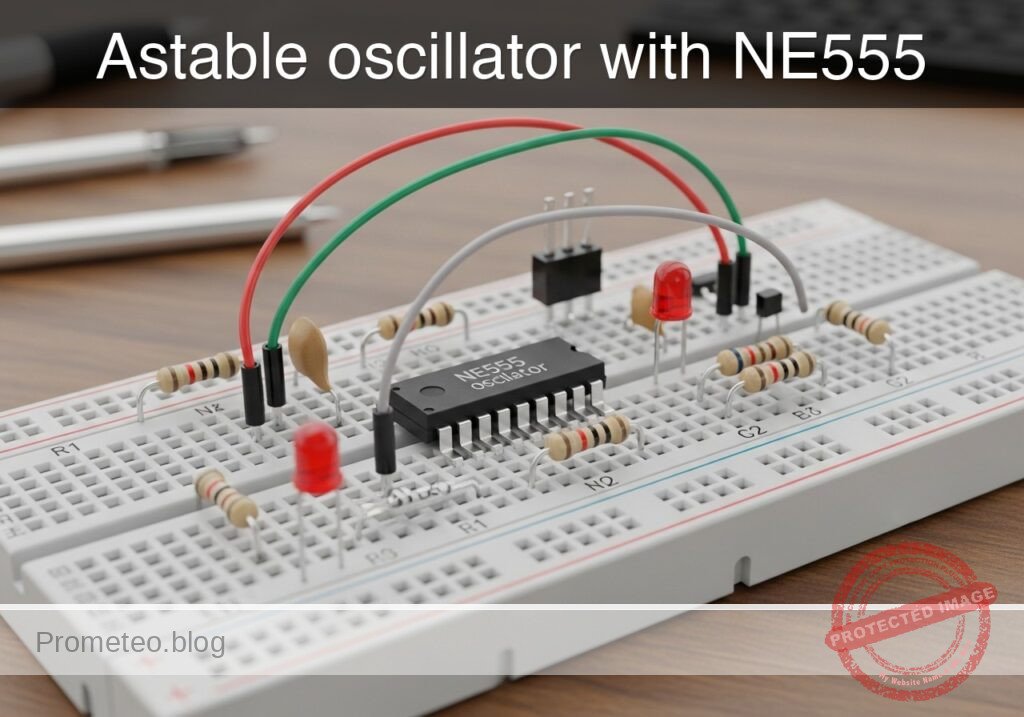
In this practical case, you will build an astable multivibrator circuit using the classic NE555 timer. The core focus is to understand how the charging and discharging of a timing capacitor regulates the frequency and duty cycle of the output signal.
Why it is useful:
* Clock generation: Generates steady clock pulses for sequential digital circuits.
* Warning flashers: Drives LEDs or lamps in hazard and warning systems.
* Audio tone generation: Produces audible frequencies for buzzers, alarms, and electronic metronomes.
* PWM foundations: Demonstrates the underlying principles needed to generate Pulse Width Modulation signals.
Expected outcome:
* The circuit will generate a continuous square wave without requiring any external trigger.
* The voltage across the timing capacitor will continuously charge and discharge between 1/3 and 2/3 of the supply voltage.
* An LED connected to the output will flash continuously at a predictable frequency of approximately 1.4 Hz.
* The frequency and duty cycle will closely match the calculated values based on the chosen RC network.
Target audience: Intermediate electronics students learning mixed-signal timing circuits and capacitor behavior.
Materials
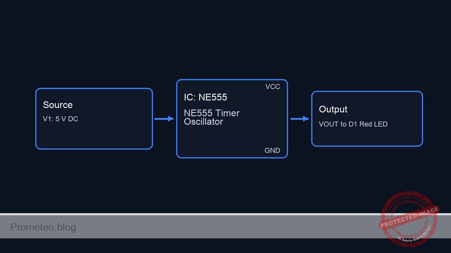
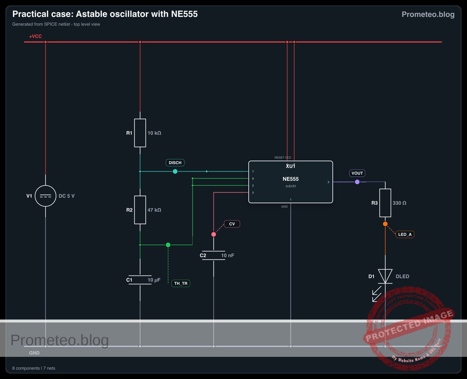
U1: NE555 timer IC, function: oscillator coreR1: 10 kΩ resistor, function: timing resistor for charge cycleR2: 47 kΩ resistor, function: timing resistor for charge and discharge cyclesC1: 10 µF electrolytic capacitor, function: primary timing capacitor determining frequencyC2: 10 nF ceramic capacitor, function: control voltage noise decouplingR3: 330 Ω resistor, function: LED current limitingD1: red LED, function: visual frequency indicatorV1: 5 V DC supply, function: circuit power
Wiring guide
V1: Connects between nodeVCC(positive) and node0(GND).U1:- Pin 8 (VCC) connects to node
VCC. - Pin 1 (GND) connects to node
0. - Pin 4 (RESET) connects to node
VCC. - Pin 2 (TRIG) and Pin 6 (THRES) are tied together to form node
TH_TR. - Pin 7 (DISCH) connects to node
DISCH. - Pin 5 (CTRL) connects to node
CV. - Pin 3 (OUT) connects to node
VOUT. R1: Connects between nodeVCCand nodeDISCH.R2: Connects between nodeDISCHand nodeTH_TR.C1: Connects between nodeTH_TR(positive lead) and node0(negative lead).C2: Connects between nodeCVand node0.R3: Connects between nodeVOUTand nodeLED_A.D1: Connects between nodeLED_A(anode) and node0(cathode).
Conceptual block diagram
Schematic
[ V1: 5 V DC ] --(PWR/RST: Pins 8,4) ------------------> [                 ]
                                                        [                 ] --(VOUT: Pin 3)--> [ R3: 330 Ω ] --(LED_A)--> [ D1: Red LED ] --> GND
[ V1: 5 V DC ] --> [ R1: 10 kΩ ] --(DISCH: Pin 7) ------> [ U1: NE555 Timer ]
                       |                                [ Oscillator Core ] --(CV: Pin 5)----> [ C2: 10nF ] --> GND
                       +--> [ R2: 47 kΩ ] --(TH_TR: 2,6)>[                 ]
                                  |                     [   (Pin 1: GND)  ]
                                  +--> [ C1: 10µF ] --> GND       |
                                                                 GND
Electrical diagram
Measurements and tests
- V-capacitor-waveform validation: Connect an oscilloscope probe to node
TH_TRand the ground lead to node0. You should observe a continuous, triangular-like waveform that charges up to roughly 3.33 V (2/3 VCC) and discharges down to roughly 1.66 V (1/3 VCC). - Frequency-Hz measurement: Connect the oscilloscope or a multimeter with frequency measurement capabilities to node
VOUT. You should read a frequency of approximately 1.38 Hz, generating a clear, visible flashing on the LED. - Duty cycle verification: Measure the high time versus the low time on node
VOUT. Because the capacitor charges through bothR1andR2but discharges only throughR2, the high time will be slightly longer than the low time (duty cycle > 50%). - Supply voltage independence test: Temporarily increase
V1from 5 V to 9 V. Observe the frequency atVOUT. The frequency should remain virtually unchanged because the internal comparator thresholds scale proportionally with the supply voltage.
SPICE netlist and simulation
Reference SPICE Netlist (ngspice) — excerptFull SPICE netlist (ngspice)
* Practical case: Astable oscillator with NE555
.width out=256

* Power Supply
V1 VCC 0 DC 5

* NE555 Timer IC Subcircuit Instance
* Pins: GND TRIG OUT RESET CTRL THRES DISCH VCC_PIN
XU1 0 TH_TR VOUT VCC CV TH_TR DISCH VCC NE555

* Timing Components
R1 VCC DISCH 10k
R2 DISCH TH_TR 47k
C1 TH_TR 0 10u
C2 CV 0 10n

* Output Load (LED)
R3 VOUT LED_A 330
D1 LED_A 0 DLED

* ... (truncated in public view) ...
Copy this content into a .cir file and run with ngspice.
* Practical case: Astable oscillator with NE555
.width out=256

* Power Supply
V1 VCC 0 DC 5

* NE555 Timer IC Subcircuit Instance
* Pins: GND TRIG OUT RESET CTRL THRES DISCH VCC_PIN
XU1 0 TH_TR VOUT VCC CV TH_TR DISCH VCC NE555

* Timing Components
R1 VCC DISCH 10k
R2 DISCH TH_TR 47k
C1 TH_TR 0 10u
C2 CV 0 10n

* Output Load (LED)
R3 VOUT LED_A 330
D1 LED_A 0 DLED

* Models
.MODEL DLED D(IS=1e-19 N=1.6 RS=10 BV=5 IBV=10u)

* Behavioral NE555 Subcircuit
.SUBCKT NE555 GND TRIG OUT RESET CTRL THRES DISCH VCC_PIN
* Internal voltage divider (3 x 5k resistors)
R1 VCC_PIN CTRL 5k
R2 CTRL N1 5k
R3 N1 GND 5k

* Smooth comparators for threshold, trigger, and reset
B_COMP_TH COMP_TH GND V=0.5*(1+tanh(100*(V(THRES,GND)-V(CTRL,GND))))
B_COMP_TR COMP_TR GND V=0.5*(1+tanh(100*(V(N1,GND)-V(TRIG,GND))))
B_COMP_RST COMP_RST GND V=0.5*(1+tanh(100*(0.7-V(RESET,GND))))

* SR Latch (Integrator with positive feedback for infinite hold time)
B_LATCH GND LATCH I=V(COMP_TR,GND) - V(COMP_TH,GND) - 5*V(COMP_RST,GND) + (V(LATCH,GND)>0.5 ? 0.1 : -0.1)
C_LATCH LATCH GND 1n
R_LATCH LATCH GND 100Meg

* Latch Voltage Clamps (Clamps V(LATCH) between ~0V and ~1V)
D1 GND LATCH D_CLAMP
V_CLAMP V_CLAMP_NODE GND 1
D2 LATCH V_CLAMP_NODE D_CLAMP
.model D_CLAMP D(N=0.01 RS=1)

* Output Driver Stage
B_OUT OUT_INT GND V=V(LATCH,GND)>0.5 ? V(VCC_PIN,GND) : 0.1
R_OUT OUT_INT OUT 10

* Open-Collector Discharge Transistor (Modeled as a Switch)
B_DISCH_CTRL DISCH_CTRL GND V=V(LATCH,GND)<0.5 ? 1 : 0
S_DISCH DISCH GND DISCH_CTRL GND SW_DISCH
.model SW_DISCH SW(VT=0.5 RON=15 ROFF=100Meg)
.ENDS

* Force initial condition on timing capacitor to ensure guaranteed oscillator startup
.ic V(TH_TR)=0

* Simulation Commands
.op
.tran 1m 3
.print tran V(VOUT) V(TH_TR) V(DISCH) V(LED_A) V(CV)
Simulation Results (Transient Analysis)

Show raw data table (3013 rows)
Index   time            v(vout)         v(th_tr)        v(disch)        v(led_a)        v(cv)
0	0.000000e+00	4.903386e+00	0.000000e+00	4.122467e+00	1.715117e+00	3.333333e+00
1	1.000000e-05	4.903386e+00	8.771053e-05	4.122482e+00	1.715117e+00	3.333333e+00
2	2.000000e-05	4.903386e+00	1.754195e-04	4.122498e+00	1.715117e+00	3.333333e+00
3	4.000000e-05	4.903386e+00	3.508344e-04	4.122529e+00	1.715117e+00	3.333333e+00
4	8.000000e-05	4.903386e+00	7.016457e-04	4.122590e+00	1.715117e+00	3.333333e+00
5	1.600000e-04	4.903386e+00	1.403195e-03	4.122713e+00	1.715117e+00	3.333333e+00
6	3.200000e-04	4.903386e+00	2.805997e-03	4.122959e+00	1.715117e+00	3.333333e+00
7	6.400000e-04	4.903386e+00	5.610420e-03	4.123451e+00	1.715117e+00	3.333333e+00
8	1.280000e-03	4.903386e+00	1.121455e-02	4.124434e+00	1.715117e+00	3.333333e+00
9	2.280000e-03	4.903386e+00	1.995841e-02	4.125968e+00	1.715117e+00	3.333333e+00
10	3.280000e-03	4.903386e+00	2.868694e-02	4.127499e+00	1.715117e+00	3.333333e+00
11	4.280000e-03	4.903386e+00	3.740018e-02	4.129028e+00	1.715117e+00	3.333333e+00
12	5.280000e-03	4.903386e+00	4.609814e-02	4.130554e+00	1.715117e+00	3.333333e+00
13	6.280000e-03	4.903386e+00	5.478085e-02	4.132077e+00	1.715117e+00	3.333333e+00
14	7.280000e-03	4.903386e+00	6.344835e-02	4.133597e+00	1.715117e+00	3.333333e+00
15	8.280000e-03	4.903386e+00	7.210065e-02	4.135115e+00	1.715117e+00	3.333333e+00
16	9.280000e-03	4.903386e+00	8.073778e-02	4.136630e+00	1.715117e+00	3.333333e+00
17	1.028000e-02	4.903386e+00	8.935978e-02	4.138143e+00	1.715117e+00	3.333333e+00
18	1.128000e-02	4.903386e+00	9.796666e-02	4.139653e+00	1.715117e+00	3.333333e+00
19	1.228000e-02	4.903386e+00	1.065585e-01	4.141160e+00	1.715117e+00	3.333333e+00
20	1.328000e-02	4.903386e+00	1.151352e-01	4.142665e+00	1.715117e+00	3.333333e+00
21	1.428000e-02	4.903386e+00	1.236969e-01	4.144166e+00	1.715117e+00	3.333333e+00
22	1.528000e-02	4.903386e+00	1.322436e-01	4.145666e+00	1.715117e+00	3.333333e+00
23	1.628000e-02	4.903386e+00	1.407753e-01	4.147162e+00	1.715117e+00	3.333333e+00
... (2989 more rows) ...
Common mistakes and how to avoid them
- Electrolytic capacitor connected backwards:
C1is an electrolytic capacitor, meaning it is polarized. If installed backwards, it will leak current, preventing it from reaching the 2/3 VCC threshold, and the circuit will freeze. Always ensure the negative stripe is connected to ground (node0). - Using too small a value for R1: If
R1is too small (e.g., less than 1 kΩ), excessive current will flow into Pin 7 during the discharge cycle. This can overheat and permanently damage the internal discharge transistor of the NE555. Always keepR1at a safe value (1 kΩ or higher). - Leaving the RESET pin floating: Pin 4 is an active-low reset. If left unconnected, ambient electrical noise can randomly reset the timer, causing erratic oscillation or stopping the circuit entirely. Always tie Pin 4 to
VCCwhen the reset function is not needed.
Troubleshooting
- Symptom: The LED stays solidly ON or OFF and never blinks.
- Cause: The timing capacitor
C1is shorted, or the wiring to Pins 2 and 6 is incomplete, preventing the trigger/threshold voltage from changing. - Fix: Verify that
C1is firmly seated and strictly connected betweenTH_TRand0. Ensure Pins 2 and 6 are bridged.
- Cause: The timing capacitor
- Symptom: The LED appears to be continuously ON but slightly dimmer than usual.
- Cause: The oscillation frequency is too high for the human eye to perceive the blinking (typically > 50 Hz). This happens if the RC values are too small.
- Fix: Check the value of
C1. If you accidentally used a 10 nF capacitor instead of a 10 µF capacitor, the frequency will be in the kilohertz range. Swap it for the correct 10 µF value.
- Symptom: The oscillation frequency is highly unstable or erratic.
- Cause: Electrical noise is interfering with the internal voltage divider of the NE555.
- Fix: Ensure
C2(10 nF) is properly connected to Pin 5 (CTRL) and ground. Also, verify that your power supplyV1is stable.
Possible improvements and extensions
- Variable frequency control: Replace
R2with a 100 kΩ potentiometer in series with a 1 kΩ fixed resistor. This allows you to manually adjust the discharge rate and, consequently, dial in the oscillation frequency on the fly. - Audio oscillator conversion: Swap
C1for a 100 nF ceramic capacitor and replace the LED/R3 network with a small 8 Ω speaker in series with a 100 µF coupling capacitor. This will shift the oscillation into the audible spectrum, creating a custom tone generator.
More Practical Cases on Prometeo.blog
Find this product and/or books on this topic on Amazon
As an Amazon Associate, I earn from qualifying purchases. If you buy through this link, you help keep this project running.
Quick Quiz

Telecommunications Electronics Engineer and Computer Engineer (official degrees in Spain).