Level: Medium | Understand magnetic energy storage to boost voltage.
Objective and use case
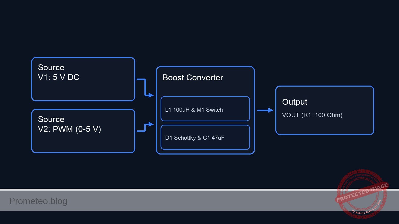
In this practical case, you will build a basic open-loop Boost converter to demonstrate how an inductor stores and releases magnetic energy to step up a DC voltage.
Why it is useful:
* Allows battery-powered devices to operate at higher voltages (e.g., generating 5 V from a single 3.7 V Li-ion cell).
* Drives strings of LEDs that require a constant, high forward voltage.
* Captures and steps up voltage in energy harvesting and regenerative braking systems.
* Provides versatile power rails in compact portable electronics without requiring multiple batteries.
Expected outcome:
* You will observe the inductor current (I_inductor) ramping up when the switch is closed and ramping down when it opens.
* The output voltage (V_out) will be demonstrably higher than the input voltage source.
* You will record the direct relationship between the switch’s Duty Cycle and the resulting V_out magnitude.
Target audience and level:
Intermediate electronics students learning the fundamentals of switch-mode power supplies.
Materials
- V1: 5 V DC source, function: main power input
- V2: Pulse voltage source (0-5 V, 100kHz, 50% duty cycle), function: PWM signal for the switch
- L1: 100 µH inductor, function: magnetic energy storage
- M1: N-channel MOSFET (e.g., IRLZ44N), function: main switching element
- D1: Schottky diode (e.g., 1N5819), function: prevents reverse current from capacitor
- C1: 47 µF capacitor, function: output voltage smoothing
- R1: 100 Ω resistor, function: basic load to discharge capacitor
Wiring guide
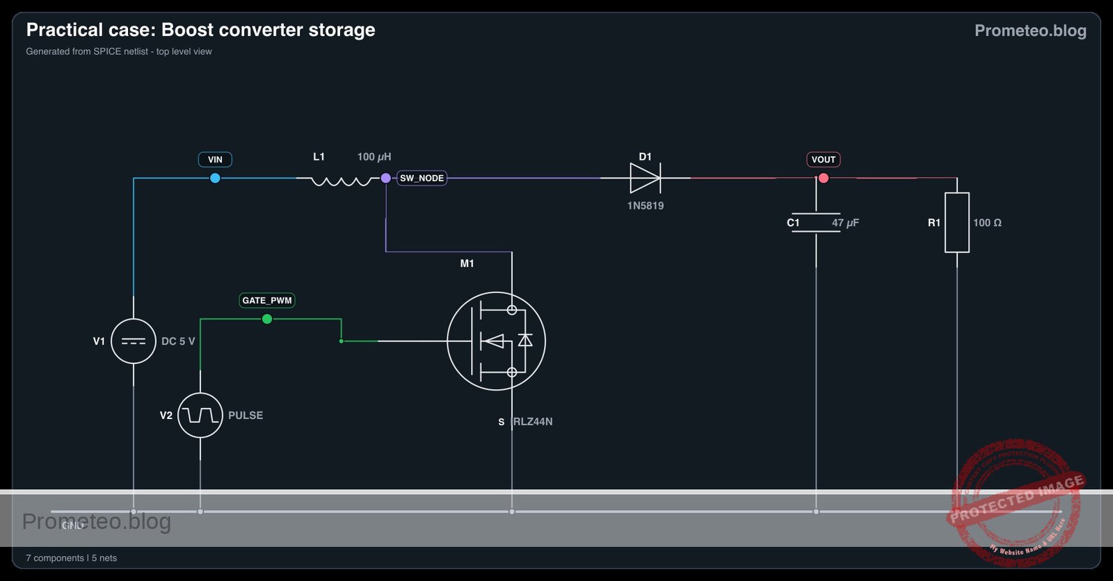
- V1: connects between VIN and 0 (GND).
- V2: connects between GATE_PWM and 0 (GND).
- L1: connects between VIN and SW_NODE.
- M1: Drain connects to SW_NODE, Gate connects to GATE_PWM, Source connects to 0 (GND).
- D1: Anode connects to SW_NODE, Cathode connects to VOUT.
- C1: connects between VOUT and 0 (GND).
- R1: connects between VOUT and 0 (GND).
Conceptual block diagram
Schematic
Control Signal:
[ V2: PWM (0-5 V) ] --(GATE_PWM)--> [ M1:Gate ]

Power & Switching Path:
[ V1: 5 V DC ] --(VIN)--> [ L1: 100µH ] --(SW_NODE)--> [ M1:Drain ] --(Switch)--> [ M1:Source ] --> GND
                                             |
Boost Output & Load:                         |
                                             +--> [ D1: Schottky ] --(VOUT)--> [ R1: 100 Ω ] --> GND
                                                                       |
                                                                       +--> [ C1: 47µF ] --> GND
Electrical diagram
Measurements and tests
- Initial state check: Apply V1 (5 V) with V2 turned off (0% duty cycle). Measure VOUT. The voltage should be roughly 4.7 V (the 5 V input minus the forward voltage drop of the Schottky diode).
- Switching activation: Activate V2 to supply a 100kHz square wave at a 50% duty cycle. Measure VOUT across R1. The voltage should rise to approximately 9 V-10 V, demonstrating the step-up action.
- Inductor current observation: Probe the current flowing through L1 (I_inductor). You will observe a triangular waveform. The upward slope occurs while M1 is ON (energy storage), and the downward slope occurs while M1 is OFF (energy release to VOUT).
- Duty Cycle mapping: Adjust the Duty Cycle of V2 from 30% to 70% in 10% increments. Record VOUT at each step to verify that a higher duty cycle yields a higher output voltage.
SPICE netlist and simulation
Reference SPICE Netlist (ngspice) — excerptFull SPICE netlist (ngspice)
* Boost converter storage

* Main power input
V1 VIN 0 DC 5

* PWM signal for the switch (100kHz, 50% duty cycle)
V2 GATE_PWM 0 PULSE(0 5 0 10n 10n 5u 10u)

* Magnetic energy storage
L1 VIN SW_NODE 100u

* Main switching element (N-channel MOSFET)
* Drain: SW_NODE, Gate: GATE_PWM, Source: 0, Bulk: 0
M1 SW_NODE GATE_PWM 0 0 IRLZ44N

* Prevents reverse current from capacitor
* Anode: SW_NODE, Cathode: VOUT
D1 SW_NODE VOUT 1N5819

* Output voltage smoothing
* ... (truncated in public view) ...
Copy this content into a .cir file and run with ngspice.
* Boost converter storage

* Main power input
V1 VIN 0 DC 5

* PWM signal for the switch (100kHz, 50% duty cycle)
V2 GATE_PWM 0 PULSE(0 5 0 10n 10n 5u 10u)

* Magnetic energy storage
L1 VIN SW_NODE 100u

* Main switching element (N-channel MOSFET)
* Drain: SW_NODE, Gate: GATE_PWM, Source: 0, Bulk: 0
M1 SW_NODE GATE_PWM 0 0 IRLZ44N

* Prevents reverse current from capacitor
* Anode: SW_NODE, Cathode: VOUT
D1 SW_NODE VOUT 1N5819

* Output voltage smoothing
C1 VOUT 0 47u

* Basic load to discharge capacitor
R1 VOUT 0 100

* Models
.model IRLZ44N NMOS(Level=1 VTO=2.0 KP=10.0 RS=0.05 RD=0.05)
.model 1N5819 D(IS=1e-6 RS=0.1 N=1.05 EG=0.69 XTI=2)

* Output Directives
* VOUT is the main output, GATE_PWM is the input stimulus
.print tran V(VOUT) V(GATE_PWM) V(SW_NODE) V(VIN) I(L1)

* Analysis
* Time constant is R*C = 4.7ms. Simulating for 10ms to observe steady-state boost voltage.
.op
.tran 0.1u 10m

.end
Simulation Results (Transient Analysis)

Show raw data table (119800 rows)
Index   time            v(vout)         v(gate_pwm)     v(sw_node)      v(vin)          l1#branch
0	0.000000e+00	4.702912e+00	0.000000e+00	5.000000e+00	5.000000e+00	4.702912e-02
1	1.000000e-10	4.702912e+00	5.000000e-02	4.999798e+00	5.000000e+00	4.702912e-02
2	2.000000e-10	4.702912e+00	1.000000e-01	4.999798e+00	5.000000e+00	4.702912e-02
3	4.000000e-10	4.702912e+00	2.000000e-01	4.999797e+00	5.000000e+00	4.702912e-02
4	8.000000e-10	4.702912e+00	4.000000e-01	4.999797e+00	5.000000e+00	4.702912e-02
5	1.600000e-09	4.702912e+00	8.000000e-01	4.999797e+00	5.000000e+00	4.702912e-02
6	3.200000e-09	4.702912e+00	1.600000e+00	4.999797e+00	5.000000e+00	4.702913e-02
7	6.400000e-09	4.702910e+00	3.200000e+00	8.651034e-03	5.000000e+00	4.710899e-02
8	1.000000e-08	4.702907e+00	5.000000e+00	6.306948e-03	5.000000e+00	4.728872e-02
9	1.064000e-08	4.702906e+00	5.000000e+00	6.311218e-03	5.000000e+00	4.732068e-02
10	1.192000e-08	4.702905e+00	5.000000e+00	6.319746e-03	5.000000e+00	4.738460e-02
11	1.448000e-08	4.702902e+00	5.000000e+00	6.336800e-03	5.000000e+00	4.751244e-02
12	1.960000e-08	4.702897e+00	5.000000e+00	6.370908e-03	5.000000e+00	4.776811e-02
13	2.984000e-08	4.702887e+00	5.000000e+00	6.439123e-03	5.000000e+00	4.827946e-02
14	5.032000e-08	4.702866e+00	5.000000e+00	6.575553e-03	5.000000e+00	4.930212e-02
15	9.128000e-08	4.702825e+00	5.000000e+00	6.848406e-03	5.000000e+00	5.134738e-02
16	1.732000e-07	4.702743e+00	5.000000e+00	7.394086e-03	5.000000e+00	5.543754e-02
17	2.732000e-07	4.702643e+00	5.000000e+00	8.060152e-03	5.000000e+00	6.042981e-02
18	3.732000e-07	4.702543e+00	5.000000e+00	8.726166e-03	5.000000e+00	6.542142e-02
19	4.732000e-07	4.702443e+00	5.000000e+00	9.392128e-03	5.000000e+00	7.041236e-02
20	5.732000e-07	4.702343e+00	5.000000e+00	1.005804e-02	5.000000e+00	7.540264e-02
21	6.732000e-07	4.702243e+00	5.000000e+00	1.072390e-02	5.000000e+00	8.039225e-02
22	7.732000e-07	4.702143e+00	5.000000e+00	1.138970e-02	5.000000e+00	8.538119e-02
23	8.732000e-07	4.702043e+00	5.000000e+00	1.205546e-02	5.000000e+00	9.036947e-02
... (119776 more rows) ...
Reference SPICE netlist (ngspice)
* Boost converter storage

* Main power input
V1 VIN 0 DC 5

* PWM signal for the switch (100kHz, 50% duty cycle)
V2 GATE_PWM 0 PULSE(0 5 0 10n 10n 5u 10u)

* Magnetic energy storage
L1 VIN SW_NODE 100u

* Main switching element (N-channel MOSFET)
* Drain: SW_NODE, Gate: GATE_PWM, Source: 0, Bulk: 0
M1 SW_NODE GATE_PWM 0 0 IRLZ44N

* Prevents reverse current from capacitor
* Anode: SW_NODE, Cathode: VOUT
D1 SW_NODE VOUT 1N5819

* Output voltage smoothing
C1 VOUT 0 47u

* Basic load to discharge capacitor
R1 VOUT 0 100

* Models
.model IRLZ44N NMOS(Level=1 VTO=2.0 KP=10.0 RS=0.05 RD=0.05)
.model 1N5819 D(IS=1e-6 RS=0.1 N=1.05 EG=0.69 XTI=2)

* Output Directives
* VOUT is the main output, GATE_PWM is the input stimulus
.print tran V(VOUT) V(GATE_PWM) V(SW_NODE) V(VIN) I(L1)

* Analysis
* Time constant is R*C = 4.7ms. Simulating for 10ms to observe steady-state boost voltage.
.op
.tran 0.1u 10m

.end
Simulation Results (Transient Analysis)
Common mistakes and how to avoid them
- Using a standard rectifier diode (e.g., 1N4007): Standard diodes are too slow to turn off at 100kHz, leading to massive switching losses and poor voltage conversion. Always use a fast-recovery or Schottky diode like the 1N5819.
- Inductor core saturation: If the inductor’s maximum current rating is lower than the peak switching current, the magnetic core will saturate. The inductor will then act as a short circuit, potentially destroying the MOSFET. Always verify the inductor’s saturation current rating.
- Operating without a load: Running a boost converter with no load resistor (R1) can cause the output voltage to continuously rise with every switching cycle, theoretically reaching infinity and destroying the output capacitor or MOSFET. Always include a minimum load.
Troubleshooting
- Symptom: Output voltage equals the input voltage (minus diode drop).
- Cause: The MOSFET is not switching. V2 might be disconnected or the voltage level is too low to surpass the MOSFET’s gate threshold.
- Fix: Check the GATE_PWM signal with an oscilloscope. Use a logic-level MOSFET if your PWM signal is limited to 3.3 V or 5 V.
- Symptom: MOSFET becomes extremely hot very quickly.
- Cause: The inductor is saturating, or the MOSFET has a high ON-resistance (RDS(on)) and is experiencing high conduction losses.
- Fix: Swap the inductor for one with a higher current rating. Ensure the gate drive voltage is sufficient to turn the MOSFET completely ON.
- Symptom: Unstable or highly rippled output voltage.
- Cause: The output capacitor C1 is too small for the load or has a high Equivalent Series Resistance (ESR).
- Fix: Increase the capacitance of C1 or place a ceramic capacitor in parallel with the electrolytic capacitor to lower the overall ESR.
Possible improvements and extensions
- Closed-loop control: Add a voltage divider at the output connected to an error amplifier or microcontroller analog input. Dynamically adjust the PWM duty cycle to maintain a constant VOUT regardless of changes in R1 (the load).
- Synchronous rectification: Replace the Schottky diode D1 with a second P-channel or driven N-channel MOSFET. Switching this second MOSFET synchronously (inversely to M1) reduces the voltage drop typical of a diode, significantly improving overall converter efficiency.
More Practical Cases on Prometeo.blog
Find this product and/or books on this topic on Amazon
As an Amazon Associate, I earn from qualifying purchases. If you buy through this link, you help keep this project running.
Quick Quiz

Telecommunications Electronics Engineer and Computer Engineer (official degrees in Spain).