
Level: Medium | Objective: Analyze the transient voltage generated when disconnecting an inductor and mitigate it using a flyback diode.
Objective and use case
In this practical case, you will build a switched inductor circuit monitored by an oscilloscope to observe the destructive voltage spike (inductive kickback) that occurs when current is abruptly interrupted. You will then install a flyback diode in parallel with the inductive load to safely clamp this transient voltage.
Why it is useful:
* Prevents catastrophic overvoltage damage to sensitive switching components such as transistors, MOSFETs, and microcontroller pins.
* Significantly reduces electromagnetic interference (EMI) and radio frequency interference (RFI) caused by high-voltage arcing across mechanical switch contacts.
* Increases the reliability, safety, and lifespan of power supply systems, motor controllers, and relay-driven circuits.
Expected outcome:
* Without the diode, opening the switch will produce a massive negative voltage spike on the oscilloscope, often reaching hundreds of volts.
* With the flyback diode installed, the transient spike will be immediately clamped to a safe level of approximately -0.7 V.
* The stored magnetic energy will safely dissipate as a steadily decaying circulating current through the inductor-resistor-diode loop.
Target audience and level: Intermediate electronics students learning about reactive components, energy storage, and circuit protection techniques.
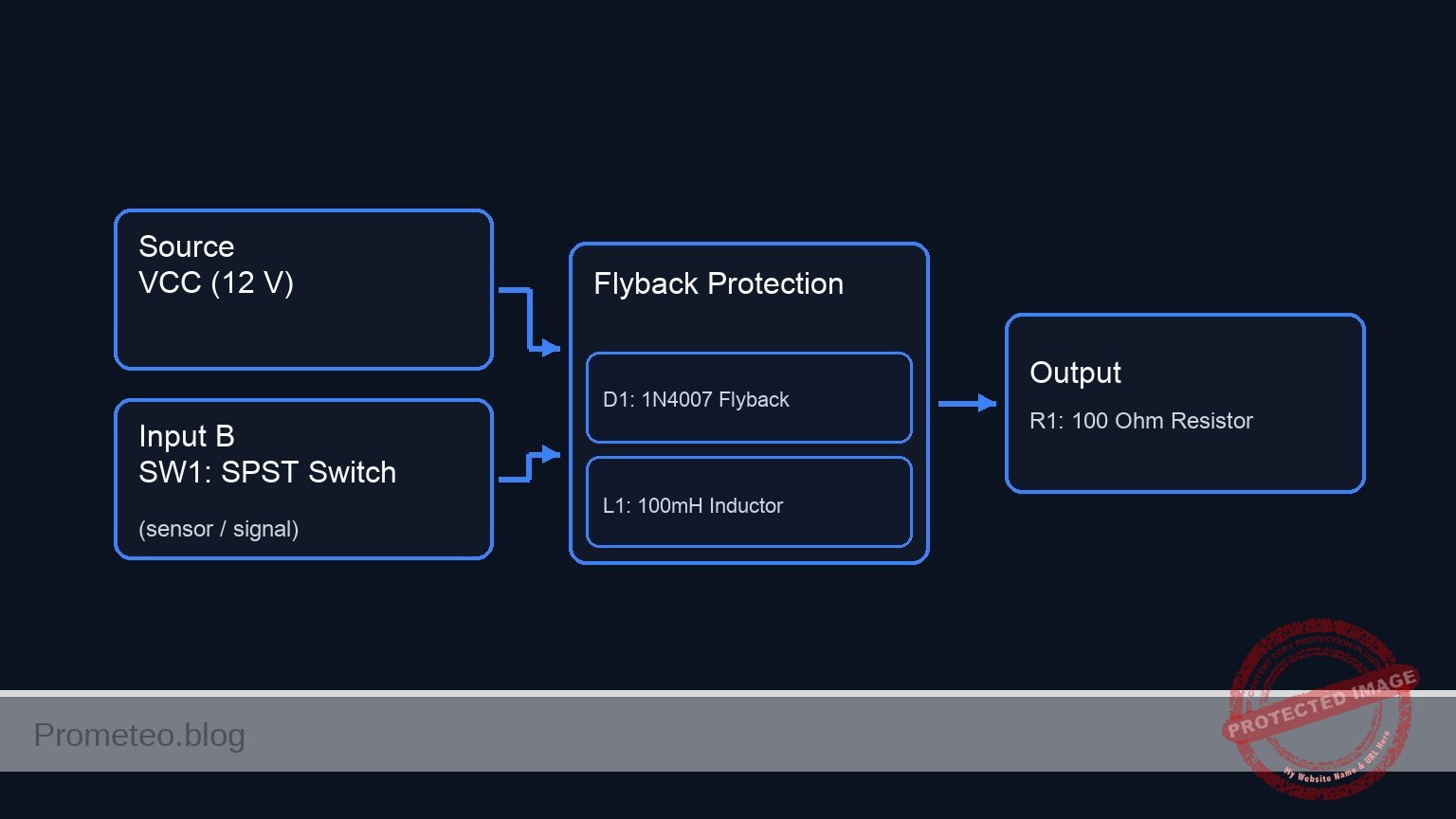
Materials
- V1: 12 V DC supply, function: main power source
- SW1: SPST toggle or push-button switch, function: circuit connection control
- L1: 100 mH inductor, function: magnetic energy storage
- R1: 100 Ω resistor, function: limits steady-state current to 120 mA
- D1: 1N4007 rectifier diode, function: flyback protection
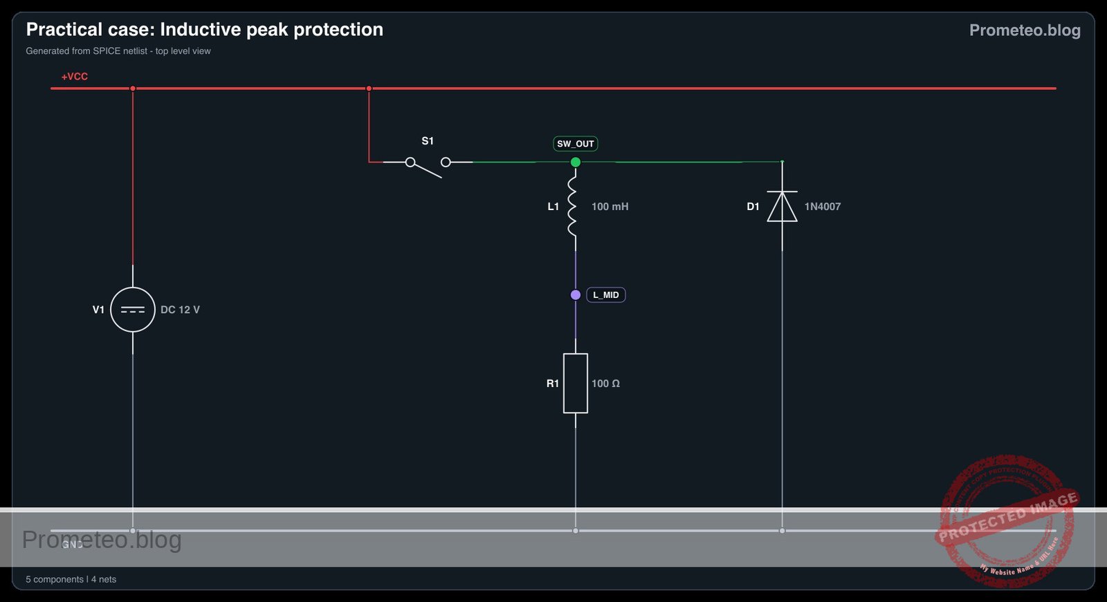
Wiring guide
- V1: connects between node VCC (positive) and node 0 (ground).
- SW1: connects between node VCC and node SW_OUT.
- L1: connects between node SW_OUT and node L_MID.
- R1: connects between node L_MID and node 0.
- D1: connects between node 0 (Anode) and node SW_OUT (Cathode) for reverse bias during normal closed-switch operation.
Conceptual block diagram
Schematic
VCC (12 V) --> [ SW1: SPST Switch ] --(SW_OUT)--> [ L1: 100mH Inductor ] --(L_MID)--> [ R1: 100 Ω Resistor ] --> GND
                                         ^
                                         |
                              (Cathode)  |
                           [ D1: 1N4007 Flyback ]
                              (Anode)    ^
                                         |
                                        GND
Electrical diagram
Measurements and tests
- Connect the oscilloscope probe to node SW_OUT and attach the ground clip to node 0. Set the oscilloscope trigger to a falling edge, single-shot mode.
- Begin with the flyback diode (D1) completely disconnected from the circuit.
- Close the switch (SW1) to allow current to flow. Wait a moment for the magnetic field in the inductor to fully build up.
- Quickly open the switch (SW1). Observe the oscilloscope capture; you will see a massive negative voltage transient as the inductor acts as a current source, forcing current across the open switch gap.
- Connect the flyback diode (D1), verifying that the cathode (striped end) connects to node SW_OUT and the anode connects to node 0.
- Repeat the switching process. The oscilloscope trace will now show the negative transient safely clamped at roughly -0.7 V as the diode forward-biases to provide a safe discharge path.
SPICE netlist and simulation
Reference SPICE Netlist (ngspice) — excerptFull SPICE netlist (ngspice)
* Inductive peak protection
.width out=256

V1 VCC 0 DC 12

* SW1 modeled as a voltage-controlled switch connecting VCC to SW_OUT
S1 VCC SW_OUT SW_CTRL 0 SW_MODEL
V_SW_CTRL SW_CTRL 0 PULSE(0 5 100u 1u 1u 500u 1000u)
.model SW_MODEL SW(VT=2.5 VH=0.1 RON=0.01 ROFF=100Meg)

L1 SW_OUT L_MID 100m
R1 L_MID 0 100

* ... (truncated in public view) ...
Copy this content into a .cir file and run with ngspice.
* Inductive peak protection
.width out=256

V1 VCC 0 DC 12

* SW1 modeled as a voltage-controlled switch connecting VCC to SW_OUT
S1 VCC SW_OUT SW_CTRL 0 SW_MODEL
V_SW_CTRL SW_CTRL 0 PULSE(0 5 100u 1u 1u 500u 1000u)
.model SW_MODEL SW(VT=2.5 VH=0.1 RON=0.01 ROFF=100Meg)

L1 SW_OUT L_MID 100m
R1 L_MID 0 100

* Flyback protection diode
D1 0 SW_OUT 1N4007
.model 1N4007 D(IS=1e-9 N=1.9 RS=0.03 BV=1000 IBV=5e-08 CJO=10p VJ=0.7 M=0.5 TT=1e-07)

.op
.tran 1u 2000u
.print tran V(SW_CTRL) V(SW_OUT) V(L_MID) V(VCC) I(L1)

.end
Simulation Results (Transient Analysis)

Show raw data table (2088 rows)
Index   time            v(sw_ctrl)      v(sw_out)       v(l_mid)        v(vcc)          l1#branch
0	0.000000e+00	0.000000e+00	1.199996e-05	1.199996e-05	1.200000e+01	1.199996e-07
1	1.000000e-08	0.000000e+00	1.199996e-05	1.199996e-05	1.200000e+01	1.199996e-07
2	2.000000e-08	0.000000e+00	1.199996e-05	1.199996e-05	1.200000e+01	1.199996e-07
3	4.000000e-08	0.000000e+00	1.199996e-05	1.199996e-05	1.200000e+01	1.199996e-07
4	8.000000e-08	0.000000e+00	1.199996e-05	1.199996e-05	1.200000e+01	1.199996e-07
5	1.600000e-07	0.000000e+00	1.199996e-05	1.199996e-05	1.200000e+01	1.199996e-07
6	3.200000e-07	0.000000e+00	1.199996e-05	1.199996e-05	1.200000e+01	1.199996e-07
7	6.400000e-07	0.000000e+00	1.199996e-05	1.199996e-05	1.200000e+01	1.199996e-07
8	1.280000e-06	0.000000e+00	1.199996e-05	1.199996e-05	1.200000e+01	1.199996e-07
9	2.280000e-06	0.000000e+00	1.199996e-05	1.199996e-05	1.200000e+01	1.199996e-07
10	3.280000e-06	0.000000e+00	1.199996e-05	1.199996e-05	1.200000e+01	1.199996e-07
11	4.280000e-06	0.000000e+00	1.199996e-05	1.199996e-05	1.200000e+01	1.199996e-07
12	5.280000e-06	0.000000e+00	1.199996e-05	1.199996e-05	1.200000e+01	1.199996e-07
13	6.280000e-06	0.000000e+00	1.199996e-05	1.199996e-05	1.200000e+01	1.199996e-07
14	7.280000e-06	0.000000e+00	1.199996e-05	1.199996e-05	1.200000e+01	1.199996e-07
15	8.280000e-06	0.000000e+00	1.199996e-05	1.199996e-05	1.200000e+01	1.199996e-07
16	9.280000e-06	0.000000e+00	1.199996e-05	1.199996e-05	1.200000e+01	1.199996e-07
17	1.028000e-05	0.000000e+00	1.199996e-05	1.199996e-05	1.200000e+01	1.199996e-07
18	1.128000e-05	0.000000e+00	1.199996e-05	1.199996e-05	1.200000e+01	1.199996e-07
19	1.228000e-05	0.000000e+00	1.199996e-05	1.199996e-05	1.200000e+01	1.199996e-07
20	1.328000e-05	0.000000e+00	1.199996e-05	1.199996e-05	1.200000e+01	1.199996e-07
21	1.428000e-05	0.000000e+00	1.199996e-05	1.199996e-05	1.200000e+01	1.199996e-07
22	1.528000e-05	0.000000e+00	1.199996e-05	1.199996e-05	1.200000e+01	1.199996e-07
23	1.628000e-05	0.000000e+00	1.199996e-05	1.199996e-05	1.200000e+01	1.199996e-07
... (2064 more rows) ...
Reference SPICE netlist (ngspice)
* Inductive peak protection
.width out=256

V1 VCC 0 DC 12

* SW1 modeled as a voltage-controlled switch connecting VCC to SW_OUT
S1 VCC SW_OUT SW_CTRL 0 SW_MODEL
V_SW_CTRL SW_CTRL 0 PULSE(0 5 100u 1u 1u 500u 1000u)
.model SW_MODEL SW(VT=2.5 VH=0.1 RON=0.01 ROFF=100Meg)

L1 SW_OUT L_MID 100m
R1 L_MID 0 100

* Flyback protection diode
D1 0 SW_OUT 1N4007
.model 1N4007 D(IS=1e-9 N=1.9 RS=0.03 BV=1000 IBV=5e-08 CJO=10p VJ=0.7 M=0.5 TT=1e-07)

.op
.tran 1u 2000u
.print tran V(SW_CTRL) V(SW_OUT) V(L_MID) V(VCC) I(L1)

.end
Simulation Results (Transient Analysis)
Common mistakes and how to avoid them
- Reversing the diode polarity: Placing the diode with the anode pointing to the positive voltage node creates a direct short circuit to ground when the switch is closed. This will destroy the diode or trigger the power supply’s overcurrent protection. Always ensure the cathode faces the higher potential.
- Using a diode with inadequate current rating: The flyback diode must safely handle a peak forward current equal to the steady-state current of the inductor just before switching. Always use properly rated rectifier, Schottky, or fast-recovery diodes.
- Omitting the series resistor: Connecting a pure inductor directly across a high-current DC source acts as a near short-circuit once the magnetic field is fully established. Always include a current-limiting series resistor, or ensure the inductor (such as a relay coil) has sufficient internal DC resistance.
Troubleshooting
- Symptom: The power supply shuts down or its current limit LED turns on immediately upon closing the switch.
- Cause: The flyback diode is installed backwards, creating a short circuit from the power source to ground.
- Fix: Disconnect power immediately and flip the diode so its striped end (cathode) faces the switch node.
- Symptom: A massive voltage spike still appears on the oscilloscope even with the diode supposedly installed.
- Cause: The diode may have blown open due to a previous overcurrent event, or the breadboard connection is loose.
- Fix: Verify diode continuity using a multimeter’s diode mode, and check the physical seating of the pins at the switch and ground nodes.
- Symptom: The oscilloscope trace shows high-frequency ringing instead of a clean clamp.
- Cause: Parasitic capacitance in the switch, wiring, or oscilloscope probes interacting with the inductor.
- Fix: Ensure the oscilloscope probe is properly compensated (x10 mode recommended for high voltage spikes) and keep ground leads as short as physically possible.
Possible improvements and extensions
- Automated switching with a MOSFET: Replace the mechanical switch with an N-channel MOSFET driven by a square wave generator (configured as a low-side switch) to observe repetitive clamping on the oscilloscope in real-time.
- Fast discharge using a Zener diode: Add an appropriately rated Zener diode in series with the standard flyback diode (anode connected to anode). This allows the inductor to discharge its energy much faster by clamping the voltage at a higher, but strictly controlled, level.
More Practical Cases on Prometeo.blog
Find this product and/or books on this topic on Amazon
As an Amazon Associate, I earn from qualifying purchases. If you buy through this link, you help keep this project running.
Quick Quiz

Telecommunications Electronics Engineer and Computer Engineer (official degrees in Spain).