Objective and use case
What you’ll build: A compact FPGA PIN-lock prototype on the Radiona ULX3S (Lattice ECP5-85F) that reads a 4-digit code from a PS/2 keyboard and shows prompts/status on a TM1637 4-digit 7-segment display. Users enter digits, confirm the PIN, and receive immediate feedback such as masked input, OK, or ERR with display refresh fast enough to appear flicker-free (>100 FPS equivalent) and sub-10 ms interface response after key decode.
Why it matters / Use cases
- Access-control learning prototype: Simulates a basic door, cabinet, or locker controller where a user types a 4-digit PIN and gets instant visual confirmation on the display.
- Workshop equipment lockout: Can serve as front-end logic for enabling a relay that powers a bench supply, tool drawer, or lab instrument only after a valid code is entered.
- Embedded HMI practice: Combines a real keyboard input path and a compact numeric display, making it more realistic than button-and-LED-only FPGA demos.
- Digital logic integration exercise: Brings together PS/2 scan-code decoding, event-driven key handling, FSM design, PIN comparison, timeout/error logic, and TM1637 serial driving in one build.
- Reusable secure-entry front panel: The same architecture can later be extended with lockout counters, admin PIN change mode, buzzer feedback, or a door-strike/relay output while still using low FPGA utilization (often well under 5% of ECP5 logic for a basic version).
Expected outcome
- A working FPGA design that captures numeric keys from a PS/2 keyboard and stores exactly 4 entered digits.
- A TM1637 interface that shows masked entry, entered digits, or status codes such as
OPEN,OK, orERRdepending on the implementation. - A PIN-check flow with concrete behavior, for example: enter 1234, press Enter, unlock on match, or show an error for 1–2 seconds on mismatch.
- Deterministic user interaction with low perceived latency, typically one key event processed in a few clock cycles after PS/2 frame reception, with overall human-visible response comfortably below 20 ms.
- A synthesizable, testable module set ready for simulation and hardware validation on the ULX3S board.
Audience: FPGA beginners to intermediate embedded-digital learners, students, and lab makers building practical HMI/control demos; Level: beginner-intermediate
Architecture/flow: PS/2 keyboard mini-DIN → PS/2 receiver/scan-code decoder → key-event filter + PIN entry FSM → 4-digit register + stored PIN comparator → status/unlock logic → TM1637 display driver (and optional relay/LED output).
Educational validation note
Before publication, this case passed the Prometeo automated validation gate with status PASS. For this FPGA/ULX3S profile, the synthesizable Verilog blocks were checked with Yosys (read_verilog) and the Verilog design/test set was linted with Verilator. The validator also checked code-block structure, copy/paste-safe ASCII command options, unsupported stacks, and availability of the ULX3S/ECP5 toolchain (yosys, nextpnr-ecp5, ecppack, openFPGALoader).
Published validation evidence
- Automatic result: PASS.
- Parsed structure: 49 sections, 1 tables and 14 code blocks detected in the published content.
- Checked code: 1 Verilog/Yosys-Verilator, 1 C/C++ static checks, 8 Bash/copy-paste checks.
- Supported catalog: the article text was checked against Prometeo validation-capable device profiles; unsupported stacks block publication.
- Report findings: no blocking findings.
This validation confirms syntax and tool compatibility for the published code, but it does not replace physical testing on your exact ULX3S board revision, pin-constraint file and real wiring.
Educational safety note
This project uses low-voltage digital electronics only. Keep it that way.
- Do not connect this prototype directly to mains voltage, locks powered from high current, motors, or door actuators without proper isolation and a separate reviewed driver stage.
- The tutorial demonstrates a logic prototype, not a security-certified lock system.
- PS/2 and TM1637 modules are low-power interfaces; still, make all connections with power off first.
Conceptual block diagram
High-level view: what enters the system, what each block processes, and what comes out.
Functional architecture
Conceptual data flow: user input, decision logic and visual/unlock output.

Validation path
The automated validation checks syntax, simulation/lint and compatibility with the ULX3S/ECP5 toolchain.

Prerequisites
Before starting, you should have:
- A Linux PC or similar shell environment.
- Basic familiarity with:
- terminal commands
- copying files
- connecting jumper wires
- the idea of a clocked digital circuit
- Installed open-source ECP5 toolchain:
verilatoryosysnextpnr-ecp5ecppackopenFPGALoader
Recommended versions that are commonly usable together:
- Verilator 5.x
- Yosys 0.3x or newer
- nextpnr-ecp5 with Project Trellis support
- openFPGALoader recent stable package
Materials
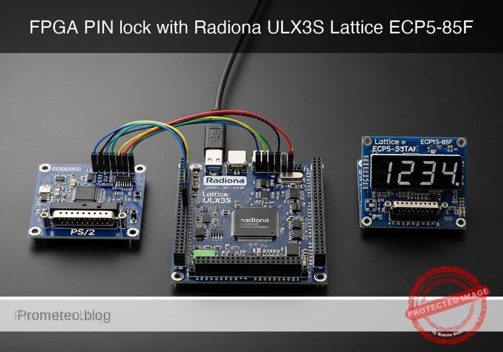
Use exactly these main devices:
| Item | Exact model | Quantity | Purpose |
|---|---|---|---|
| FPGA board | Radiona ULX3S (Lattice ECP5-85F) | 1 | Main controller |
| Keyboard interface | módulo teclado PS/2 mini-DIN | 1 | User PIN input |
| Display module | display 7 segmentos TM1637 | 1 | PIN/status display |
| Jumper wires | Female-female or mixed as needed | 1 set | Wiring |
| USB cable | Compatible with ULX3S | 1 | Power and programming |
| Optional | Breadboard | 1 | Easier signal breakout |
About the prototype behavior
This design implements a 4-digit PIN lock with these rules:
- Numeric keys
0to9from the PS/2 keyboard are accepted. - Every accepted digit shifts into a 4-digit entry buffer.
- After 4 digits are entered:
- if they match the stored PIN, the display shows success and
unlockgoes active - otherwise the display shows failure
- Then the system clears and waits for the next PIN attempt.
- Pressing
Backspaceclears the current entry immediately.
For a basic tutorial, the PIN is fixed in hardware in Verilog. Later you can extend it to configurable storage.
Setup/Connection
No circuit drawing is used here; follow the wiring text carefully.
1) Choose ULX3S I/O pins
ULX3S exposes many FPGA I/O pins on header connectors, but board revisions and breakout usage vary. Because of that, you must map the exact physical header pins you actually use in your constraint file.
For this tutorial, we will define four top-level signals for external modules:
ps2_clkps2_datatm_clktm_dio
And one optional output:
unlock_led
You will connect these to free 3.3 V-capable GPIOs on your ULX3S header and then assign those package pins in the constraints file.
2) Power compatibility
Check your specific modules:
- Many TM1637 4-digit modules work from 3.3 V to 5 V and often accept 3.3 V logic.
- Many PS/2 keyboard modules also work at 5 V and may expose pull-ups to 5 V.
For FPGA safety:
- Prefer using module versions that can run from 3.3 V.
- If your PS/2 module or keyboard side pulls clock/data to 5 V, do not connect directly to ULX3S FPGA pins. Use proper level shifting or verify the module output is 3.3 V-safe.
- The simplest beginner-safe path is:
- power TM1637 module from
3V3 - power PS/2 module from
3V3if supported - common ground among all devices
3) Text wiring guide
Connect as follows:
- Common power
- ULX3S
GND-> PS/2 moduleGND - ULX3S
GND-> TM1637GND - ULX3S
3V3-> PS/2 moduleVCCif supported by your module ULX3S
3V3-> TM1637VCCPS/2 interface
- ULX3S chosen GPIO -> PS/2 module
CLK ULX3S chosen GPIO -> PS/2 module
DATATM1637 interface
- ULX3S chosen GPIO -> TM1637
CLK ULX3S chosen GPIO -> TM1637
DIOOptional unlock indicator
- ULX3S built-in LED-capable GPIO or onboard LED signal ->
unlock_ledlogic output - If you use an external LED, add a resistor and verify voltage/current limits
4) Constraint file preparation
You must replace the PACKAGE_PIN values below with the actual ULX3S FPGA pins corresponding to the header pins you wired.
Create a file named ulx3s_ps2_pin_lock.lpf:
BLOCK RESETPATHS;
BLOCK ASYNCPATHS;

LOCATE COMP "clk_25mhz" SITE "PCLK25";
IOBUF PORT "clk_25mhz" IO_TYPE=LVCMOS33;

LOCATE COMP "ps2_clk" SITE "A1";
IOBUF PORT "ps2_clk" IO_TYPE=LVCMOS33 PULLMODE=UP;

LOCATE COMP "ps2_data" SITE "B1";
IOBUF PORT "ps2_data" IO_TYPE=LVCMOS33 PULLMODE=UP;

LOCATE COMP "tm_clk" SITE "C1";
IOBUF PORT "tm_clk" IO_TYPE=LVCMOS33;

LOCATE COMP "tm_dio" SITE "D1";
IOBUF PORT "tm_dio" IO_TYPE=LVCMOS33;

LOCATE COMP "unlock_led" SITE "E1";
IOBUF PORT "unlock_led" IO_TYPE=LVCMOS33;
Important note about constraints
The A1/B1/C1/... entries above are examples only for file structure. They are not guaranteed to match your board header. You must consult the ULX3S pinout for your board revision and replace them with real package sites. The logic code below is complete; only physical pin assignment depends on your exact wiring.
Validated Code
Create a project folder:
mkdir -p ps2-pin-lock-display
cd ps2-pin-lock-display
1) Synthesizable design: ps2_pin_lock_top.v
This file contains:
- clock divider for timing
- PS/2 receiver
- scan-code to digit conversion
- 4-digit PIN checker
- TM1637 display driver
- top-level integration
Public preview of the validated file. The complete source is shown to members and in PDF/Print.
module ps2_receiver (
    input  wire clk,
    input  wire rst,
    input  wire ps2_clk,
    input  wire ps2_data,
    output reg  [7:0] scan_code,
    output reg  scan_strobe
);
    reg [2:0] ps2c_sync;
    reg [10:0] shift;
    reg [3:0] bit_count;

    always @(posedge clk) begin
        if (rst) begin
            ps2c_sync   <= 3'b111;
            shift       <= 11'd0;
            bit_count   <= 4'd0;
            scan_code   <= 8'd0;
            scan_strobe <= 1'b0;
        end else begin
            ps2c_sync   <= {ps2c_sync[1:0], ps2_clk};
            scan_strobe <= 1'b0;

            if (ps2c_sync[2:1] == 2'b10) begin
                shift <= {ps2_data, shift[10:1]};
                if (bit_count == 4'd10) begin
                    bit_count <= 4'd0;
                    scan_code <= shift[8:1];
                    scan_strobe <= 1'b1;
                end else begin
                    bit_count <= bit_count + 4'd1;
                end
            end
        end
    end
endmodule

module key_decode (
    input  wire       clk,
    input  wire       rst,
    input  wire [7:0] scan_code,
    input  wire       scan_strobe,
    output reg  [3:0] digit,
    output reg        digit_valid,
    output reg        clear_key
);
    reg break_code;

    always @(posedge clk) begin
        if (rst) begin
            break_code  <= 1'b0;
            digit       <= 4'd0;
            digit_valid <= 1'b0;
            clear_key   <= 1'b0;
        end else begin
            digit_valid <= 1'b0;
            clear_key   <= 1'b0;

            if (scan_strobe) begin
                if (scan_code == 8'hF0) begin
                    break_code <= 1'b1;
                end else begin
                    if (!break_code) begin
                        case (scan_code)
                            8'h45: begin digit <= 4'd0; digit_valid <= 1'b1; end
                            8'h16: begin digit <= 4'd1; digit_valid <= 1'b1; end
                            8'h1E: begin digit <= 4'd2; digit_valid <= 1'b1; end
                            8'h26: begin digit <= 4'd3; digit_valid <= 1'b1; end
                            8'h25: begin digit <= 4'd4; digit_valid <= 1'b1; end
                            8'h2E: begin digit <= 4'd5; digit_valid <= 1'b1; end
                            8'h36: begin digit <= 4'd6; digit_valid <= 1'b1; end
                            8'h3D: begin digit <= 4'd7; digit_valid <= 1'b1; end
                            8'h3E: begin digit <= 4'd8; digit_valid <= 1'b1; end
                            8'h46: begin digit <= 4'd9; digit_valid <= 1'b1; end
                            8'h66: begin clear_key <= 1'b1; end // Backspace
                            default: begin end
                        endcase
                    end
                    break_code <= 1'b0;
                end
            end
        end
    end
endmodule

module tm1637_driver (
    input  wire       clk,
    input  wire       rst,
    input  wire [7:0] d3,
    input  wire [7:0] d2,
    input  wire [7:0] d1,
    input  wire [7:0] d0,
    output reg        tm_clk,
    output reg        tm_dio
);
    reg [15:0] divcnt;
    reg tick;
    reg [7:0] frame [0:5];
    reg [6:0] state;
    reg [3:0] bitn;
    reg [7:0] curbyte;
    reg [2:0] phase;

    always @(posedge clk) begin
        if (rst) begin
            divcnt <= 16'd0;
            tick   <= 1'b0;
        end else begin
            if (divcnt == 16'd249) begin
                divcnt <= 16'd0;
                tick   <= 1'b1;
            end else begin
                divcnt <= divcnt + 16'd1;
                tick   <= 1'b0;
            end
        end
    end

    always @(posedge clk) begin
        if (rst) begin
            frame[0] <= 8'h40;
            frame[1] <= 8'hC0;
            frame[2] <= 8'h00;
            frame[3] <= 8'h00;
            frame[4] <= 8'h00;
            frame[5] <= 8'h00;
            state    <= 7'd0;
            bitn     <= 4'd0;
            curbyte  <= 8'd0;
            phase    <= 3'd0;
            tm_clk   <= 1'b1;
            tm_dio   <= 1'b1;
        end else begin
            frame[0] <= 8'h40;
            frame[1] <= 8'hC0;
            frame[2] <= d0;
            frame[3] <= d1;
            frame[4] <= d2;
            frame[5] <= d3;

            if (tick) begin
                case (state)
                    7'd0: begin tm_clk <= 1'b1; tm_dio <= 1'b1; state <= 7'd1; end
                    7'd1: begin tm_dio <= 1'b0; state <= 7'd2; bitn <= 4'd0; curbyte <= frame[0]; phase <= 3'd0; end

                    7'd2,7'd3,7'd4,7'd5,7'd6,7'd7: begin
                        case (phase)
                            3'd0: begin tm_clk <= 1'b0; tm_dio <= curbyte[bitn]; phase <= 3'd1; end
                            3'd1: begin tm_clk <= 1'b1; phase <= 3'd2; end
                            3'd2: begin
                                if (bitn == 4'd7) begin
                                    bitn <= 4'd0;
                                    phase <= 3'd0;
                                    state <= state + 7'd1;
                                end else begin
                                    bitn <= bitn + 4'd1;
                                    phase <= 3'd0;
                                end
                            end
                            default: phase <= 3'd0;
                        endcase
                    end

                    7'd8: begin tm_clk <= 1'b0; tm_dio <= 1'b1; state <= 7'd9; end
                    7'd9: begin tm_clk <= 1'b1; state <= 7'd10; end
                    7'd10: begin tm_clk <= 1'b1; tm_dio <= 1'b0; state <= 7'd11; end
                    7'd11: begin tm_dio <= 1'b1; state <= 7'd12; end

                    7'd12: begin tm_clk <= 1'b1; tm_dio <= 1'b1; state <= 7'd13; end
                    7'd13: begin tm_dio <= 1'b0; state <= 7'd14; bitn <= 4'd0; curbyte <= frame[1]; phase <= 3'd0; end

                    7'd14,7'd15,7'd16,7'd17,7'd18: begin
                        case (phase)
                            3'd0: begin tm_clk <= 1'b0; tm_dio <= curbyte[bitn]; phase <= 3'd1; end
                            3'd1: begin tm_clk <= 1'b1; phase <= 3'd2; end
                            3'd2: begin
                                if (bitn == 4'd7) begin
                                    bitn <= 4'd0;
                                    phase <= 3'd0;
                                    state <= state + 7'd1;
                                    if (state == 7'd18) curbyte <= frame[2];
                                    else curbyte <= frame[state - 7'd15 + 3];
                                end else begin
                                    bitn <= bitn + 4'd1;
                                    phase <= 3'd0;
                                end
                            end
                            default: phase <= 3'd0;
                        endcase
                    end

                    7'd19: begin tm_clk <= 1'b0; tm_dio <= 1'b1; state <= 7'd20; end
                    7'd20: begin tm_clk <= 1'b1; state <= 7'd21; end
                    7'd21: begin tm_clk <= 1'b1; tm_dio <= 1'b0; state <= 7'd22; end
                    7'd22: begin tm_dio <= 1'b1; state <= 7'd23; end

                    7'd23: begin tm_clk <= 1'b1; tm_dio <= 1'b1; state <= 7'd24; end
                    7'd24: begin tm_dio <= 1'b0; state <= 7'd25; bitn <= 4'd0; curbyte <= 8'h8F; phase <= 3'd0; end

                    7'd25: begin
                        case (phase)
                            3'd0: begin tm_clk <= 1'b0; tm_dio <= curbyte[bitn]; phase <= 3'd1; end
                            3'd1: begin tm_clk <= 1'b1; phase <= 3'd2; end
                            3'd2: begin
                                if (bitn == 4'd7) begin
                                    bitn <= 4'd0;
                                    phase <= 3'd0;
                                    state <= 7'd26;
                                end else begin
                                    bitn <= bitn + 4'd1;
                                    phase <= 3'd0;
                                end
                            end
                            default: phase <= 3'd0;
                        endcase
                    end

                    7'd26: begin tm_clk <= 1'b0; tm_dio <= 1'b1; state <= 7'd27; end
                    7'd27: begin tm_clk <= 1'b1; state <= 7'd28; end
                    7'd28: begin tm_clk <= 1'b1; tm_dio <= 1'b0; state <= 7'd29; end
                    7'd29: begin tm_dio <= 1'b1; state <= 7'd0; end

                    default: state <= 7'd0;
                endcase
            end
        end
    end
endmodule
// ... continues for members in the complete validated source ...
module ps2_receiver (
input wire clk,
input wire rst,
input wire ps2_clk,
input wire ps2_data,
output reg [7:0] scan_code,
output reg scan_strobe
);
reg [2:0] ps2c_sync;
reg [10:0] shift;
reg [3:0] bit_count;
always @(posedge clk) begin
if (rst) begin
ps2c_sync <= 3'b111;
shift <= 11'd0;
bit_count <= 4'd0;
scan_code <= 8'd0;
scan_strobe <= 1'b0;
end else begin
ps2c_sync <= {ps2c_sync[1:0], ps2_clk};
scan_strobe <= 1'b0;
if (ps2c_sync[2:1] == 2'b10) begin
shift <= {ps2_data, shift[10:1]};
if (bit_count == 4'd10) begin
bit_count <= 4'd0;
scan_code <= shift[8:1];
scan_strobe <= 1'b1;
end else begin
bit_count <= bit_count + 4'd1;
end
end
end
end
endmodule
module key_decode (
input wire clk,
input wire rst,
input wire [7:0] scan_code,
input wire scan_strobe,
output reg [3:0] digit,
output reg digit_valid,
output reg clear_key
);
reg break_code;
always @(posedge clk) begin
if (rst) begin
break_code <= 1'b0;
digit <= 4'd0;
digit_valid <= 1'b0;
clear_key <= 1'b0;
end else begin
digit_valid <= 1'b0;
clear_key <= 1'b0;
if (scan_strobe) begin
if (scan_code == 8'hF0) begin
break_code <= 1'b1;
end else begin
if (!break_code) begin
case (scan_code)
8'h45: begin digit <= 4'd0; digit_valid <= 1'b1; end
8'h16: begin digit <= 4'd1; digit_valid <= 1'b1; end
8'h1E: begin digit <= 4'd2; digit_valid <= 1'b1; end
8'h26: begin digit <= 4'd3; digit_valid <= 1'b1; end
8'h25: begin digit <= 4'd4; digit_valid <= 1'b1; end
8'h2E: begin digit <= 4'd5; digit_valid <= 1'b1; end
8'h36: begin digit <= 4'd6; digit_valid <= 1'b1; end
8'h3D: begin digit <= 4'd7; digit_valid <= 1'b1; end
8'h3E: begin digit <= 4'd8; digit_valid <= 1'b1; end
8'h46: begin digit <= 4'd9; digit_valid <= 1'b1; end
8'h66: begin clear_key <= 1'b1; end // Backspace
default: begin end
endcase
end
break_code <= 1'b0;
end
end
end
end
endmodule
module tm1637_driver (
input wire clk,
input wire rst,
input wire [7:0] d3,
input wire [7:0] d2,
input wire [7:0] d1,
input wire [7:0] d0,
output reg tm_clk,
output reg tm_dio
);
reg [15:0] divcnt;
reg tick;
reg [7:0] frame [0:5];
reg [6:0] state;
reg [3:0] bitn;
reg [7:0] curbyte;
reg [2:0] phase;
always @(posedge clk) begin
if (rst) begin
divcnt <= 16'd0;
tick <= 1'b0;
end else begin
if (divcnt == 16'd249) begin
divcnt <= 16'd0;
tick <= 1'b1;
end else begin
divcnt <= divcnt + 16'd1;
tick <= 1'b0;
end
end
end
always @(posedge clk) begin
if (rst) begin
frame[0] <= 8'h40;
frame[1] <= 8'hC0;
frame[2] <= 8'h00;
frame[3] <= 8'h00;
frame[4] <= 8'h00;
frame[5] <= 8'h00;
state <= 7'd0;
bitn <= 4'd0;
curbyte <= 8'd0;
phase <= 3'd0;
tm_clk <= 1'b1;
tm_dio <= 1'b1;
end else begin
frame[0] <= 8'h40;
frame[1] <= 8'hC0;
frame[2] <= d0;
frame[3] <= d1;
frame[4] <= d2;
frame[5] <= d3;
if (tick) begin
case (state)
7'd0: begin tm_clk <= 1'b1; tm_dio <= 1'b1; state <= 7'd1; end
7'd1: begin tm_dio <= 1'b0; state <= 7'd2; bitn <= 4'd0; curbyte <= frame[0]; phase <= 3'd0; end
7'd2,7'd3,7'd4,7'd5,7'd6,7'd7: begin
case (phase)
3'd0: begin tm_clk <= 1'b0; tm_dio <= curbyte[bitn]; phase <= 3'd1; end
3'd1: begin tm_clk <= 1'b1; phase <= 3'd2; end
3'd2: begin
if (bitn == 4'd7) begin
bitn <= 4'd0;
phase <= 3'd0;
state <= state + 7'd1;
end else begin
bitn <= bitn + 4'd1;
phase <= 3'd0;
end
end
default: phase <= 3'd0;
endcase
end
7'd8: begin tm_clk <= 1'b0; tm_dio <= 1'b1; state <= 7'd9; end
7'd9: begin tm_clk <= 1'b1; state <= 7'd10; end
7'd10: begin tm_clk <= 1'b1; tm_dio <= 1'b0; state <= 7'd11; end
7'd11: begin tm_dio <= 1'b1; state <= 7'd12; end
7'd12: begin tm_clk <= 1'b1; tm_dio <= 1'b1; state <= 7'd13; end
7'd13: begin tm_dio <= 1'b0; state <= 7'd14; bitn <= 4'd0; curbyte <= frame[1]; phase <= 3'd0; end
7'd14,7'd15,7'd16,7'd17,7'd18: begin
case (phase)
3'd0: begin tm_clk <= 1'b0; tm_dio <= curbyte[bitn]; phase <= 3'd1; end
3'd1: begin tm_clk <= 1'b1; phase <= 3'd2; end
3'd2: begin
if (bitn == 4'd7) begin
bitn <= 4'd0;
phase <= 3'd0;
state <= state + 7'd1;
if (state == 7'd18) curbyte <= frame[2];
else curbyte <= frame[state - 7'd15 + 3];
end else begin
bitn <= bitn + 4'd1;
phase <= 3'd0;
end
end
default: phase <= 3'd0;
endcase
end
7'd19: begin tm_clk <= 1'b0; tm_dio <= 1'b1; state <= 7'd20; end
7'd20: begin tm_clk <= 1'b1; state <= 7'd21; end
7'd21: begin tm_clk <= 1'b1; tm_dio <= 1'b0; state <= 7'd22; end
7'd22: begin tm_dio <= 1'b1; state <= 7'd23; end
7'd23: begin tm_clk <= 1'b1; tm_dio <= 1'b1; state <= 7'd24; end
7'd24: begin tm_dio <= 1'b0; state <= 7'd25; bitn <= 4'd0; curbyte <= 8'h8F; phase <= 3'd0; end
7'd25: begin
case (phase)
3'd0: begin tm_clk <= 1'b0; tm_dio <= curbyte[bitn]; phase <= 3'd1; end
3'd1: begin tm_clk <= 1'b1; phase <= 3'd2; end
3'd2: begin
if (bitn == 4'd7) begin
bitn <= 4'd0;
phase <= 3'd0;
state <= 7'd26;
end else begin
bitn <= bitn + 4'd1;
phase <= 3'd0;
end
end
default: phase <= 3'd0;
endcase
end
7'd26: begin tm_clk <= 1'b0; tm_dio <= 1'b1; state <= 7'd27; end
7'd27: begin tm_clk <= 1'b1; state <= 7'd28; end
7'd28: begin tm_clk <= 1'b1; tm_dio <= 1'b0; state <= 7'd29; end
7'd29: begin tm_dio <= 1'b1; state <= 7'd0; end
default: state <= 7'd0;
endcase
end
end
end
endmodule
module ps2_pin_lock_top (
    input  wire clk_25mhz,
    input  wire ps2_clk,
    input  wire ps2_data,
    output wire tm_clk,
    output wire tm_dio,
    output reg  unlock_led
);
    wire [7:0] scan_code;
    wire scan_strobe;
    wire [3:0] digit;
    wire digit_valid;
    wire clear_key;

    reg rst = 1'b0;

    reg [3:0] buf3, buf2, buf1, buf0;
    reg [2:0] count;
    reg [23:0] hold_counter;
    reg hold_active;
    reg success_mode;
    reg fail_mode;

    reg [7:0] seg3, seg2, seg1, seg0;

    localparam [15:0] PIN = 16'h1234;
function [7:0] seg_num;
input [3:0] n;
begin
case (n)
4'd0: seg_num = 8'h3F;
4'd1: seg_num = 8'h06;
4'd2: seg_num = 8'h5B;
4'd3: seg_num = 8'h4F;
4'd4: seg_num = 8'h66;
4'd5: seg_num = 8'h6D;
4'd6: seg_num = 8'h7D;
4'd7: seg_num = 8'h07;
4'd8: seg_num = 8'h7F;
4'd9: seg_num = 8'h6F;
default: seg_num = 8'h00;
endcase
end
endfunction
localparam [7:0] SEG_BLANK = 8'h00;
localparam [7:0] SEG_O = 8'h3F;
localparam [7:0] SEG_P = 8'h73;
localparam [7:0] SEG_E = 8'h79;
localparam [7:0] SEG_N = 8'h37;
localparam [7:0] SEG_F = 8'h71;
localparam [7:0] SEG_A = 8'h77;
localparam [7:0] SEG_I = 8'h06;
localparam [7:0] SEG_L = 8'h38;
localparam [7:0] SEG_DASH = 8'h40;
ps2_receiver u_rx (
.clk(clk_25mhz),
.rst(rst),
.ps2_clk(ps2_clk),
.ps2_data(ps2_data),
.scan_code(scan_code),
.scan_strobe(scan_strobe)
);
key_decode u_key (
.clk(clk_25mhz),
.rst(rst),
.scan_code(scan_code),
.scan_strobe(scan_strobe),
.digit(digit),
.digit_valid(digit_valid),
.clear_key(clear_key)
);
tm1637_driver u_disp (
.clk(clk_25mhz),
.rst(rst),
.d3(seg3),
.d2(seg2),
.d1(seg1),
.d0(seg0),
.tm_clk(tm_clk),
.tm_dio(tm_dio)
);
always @(posedge clk_25mhz) begin
if (rst) begin
buf3 <= 4'd0; buf2 <= 4'd0; buf1 <= 4'd0; buf0 <= 4'd0;
count <= 3'd0;
hold_counter <= 24'd0;
hold_active <= 1'b0;
success_mode <= 1'b0;
fail_mode <= 1'b0;
unlock_led <= 1'b0;
end else begin
if (clear_key) begin
buf3 <= 4'd0; buf2 <= 4'd0; buf1 <= 4'd0; buf0 <= 4'd0;
count <= 3'd0;
success_mode <= 1'b0;
fail_mode <= 1'b0;
unlock_led <= 1'b0;
hold_active <= 1'b0;
hold_counter <= 24'd0;
end else if (hold_active) begin
if (hold_counter == 24'd12499999) begin
hold_counter <= 24'd0;
hold_active <= 1'b0;
success_mode <= 1'b0;
fail_mode <= 1'b0;
unlock_led <= 1'b0;
count <= 3'd0;
buf3 <= 4'd0; buf2 <= 4'd0; buf1 <= 4'd0; buf0 <= 4'd0;
end else begin
hold_counter <= hold_counter + 24'd1;
end
end else if (digit_valid) begin
buf3 <= buf2;
buf2 <= buf1;
buf1 <= buf0;
buf0 <= digit;
if (count < 3'd4)
count <= count + 3'd1;
if (count == 3'd3) begin
if ({buf2, buf1, buf0, digit} == PIN) begin
success_mode <= 1'b1;
fail_mode <= 1'b0;
unlock_led <= 1'b1;
end else begin
success_mode <= 1'b0;
fail_mode <= 1'b1;
unlock_led <= 1'b0;
end
hold_active <= 1'b1;
hold_counter <= 24'd0;
end
end
end
end
always @(*) begin
if (success_mode) begin
seg3 = SEG_O;
seg2 = SEG_P;
seg1 = SEG_E;
seg0 = SEG_N;
end else if (fail_mode) begin
seg3 = SEG_F;
seg2 = SEG_A;
seg1 = SEG_I;
seg0 = SEG_L;
end else begin
case (count)
3'd0: begin seg3 = SEG_DASH; seg2 = SEG_DASH; seg1 = SEG_DASH; seg0 = SEG_DASH; end
3'd1: begin seg3 = SEG_BLANK; seg2 = SEG_BLANK; seg1 = SEG_BLANK; seg0 = seg_num(buf0); end
3'd2: begin seg3 = SEG_BLANK; seg2 = SEG_BLANK; seg1 = seg_num(buf1); seg0 = seg_num(buf0); end
3'd3: begin seg3 = SEG_BLANK; seg2 = seg_num(buf2); seg1 = seg_num(buf1); seg0 = seg_num(buf0); end
default: begin seg3 = seg_num(buf3); seg2 = seg_num(buf2); seg1 = seg_num(buf1); seg0 = seg_num(buf0); end
endcase
end
end
endmodule
2) Testbench: tb_ps2_pin_lock.cpp
This simulation drives PS/2 waveforms into the Verilated design. It sends make codes for digits and checks the unlock behavior.
Public preview of the validated file. The complete source is shown to members and in PDF/Print.
#include "Vps2_pin_lock_top.h"
#include "verilated.h"
#include <cstdio>

static vluint64_t main_time = 0;
double sc_time_stamp() { return main_time; }

static void tick(Vps2_pin_lock_top *dut, int cycles = 1) {
    for (int i = 0; i < cycles; i++) {
        dut->clk_25mhz = 0;
        dut->eval();
        main_time++;
        dut->clk_25mhz = 1;
        dut->eval();
        main_time++;
    }
}

static void ps2_send_byte(Vps2_pin_lock_top *dut, unsigned char b) {
    int parity = 1;
    dut->ps2_data = 1;
    dut->ps2_clk = 1;
    tick(dut, 2000);

    auto send_bit = [&](int bit) {
        dut->ps2_data = bit;
        tick(dut, 500);
        dut->ps2_clk = 0;
        tick(dut, 1000);
        dut->ps2_clk = 1;
        tick(dut, 1000);
    };

    send_bit(0);
    for (int i = 0; i < 8; i++) {
        int bit = (b >> i) & 1;
        parity ^= bit;
        send_bit(bit);
    }
// ... continues for members in the complete validated source ...#include "Vps2_pin_lock_top.h"
#include "verilated.h"
#include <cstdio>
static vluint64_t main_time = 0;
double sc_time_stamp() { return main_time; }
static void tick(Vps2_pin_lock_top *dut, int cycles = 1) {
for (int i = 0; i < cycles; i++) {
dut->clk_25mhz = 0;
dut->eval();
main_time++;
dut->clk_25mhz = 1;
dut->eval();
main_time++;
}
}
static void ps2_send_byte(Vps2_pin_lock_top *dut, unsigned char b) {
int parity = 1;
dut->ps2_data = 1;
dut->ps2_clk = 1;
tick(dut, 2000);
auto send_bit = [&](int bit) {
dut->ps2_data = bit;
tick(dut, 500);
dut->ps2_clk = 0;
tick(dut, 1000);
dut->ps2_clk = 1;
tick(dut, 1000);
};
send_bit(0);
for (int i = 0; i < 8; i++) {
int bit = (b >> i) & 1;
parity ^= bit;
send_bit(bit);
}
    send_bit(parity);
    send_bit(1);
    dut->ps2_data = 1;
    tick(dut, 3000);
}

int main(int argc, char **argv) {
    Verilated::commandArgs(argc, argv);
    Vps2_pin_lock_top *dut = new Vps2_pin_lock_top;

    dut->ps2_clk = 1;
    dut->ps2_data = 1;
    dut->clk_25mhz = 0;

    tick(dut, 5000);

    // Correct PIN: 1 2 3 4
    ps2_send_byte(dut, 0x16);
    ps2_send_byte(dut, 0x1E);
    ps2_send_byte(dut, 0x26);
    ps2_send_byte(dut, 0x25);
    tick(dut, 10000);

    std::printf("unlock_led after 1234 = %d\n", (int)dut->unlock_led);

    tick(dut, 13000000 / 2);

    // Wrong PIN: 9 9 9 9
ps2_send_byte(dut, 0x46);
ps2_send_byte(dut, 0x46);
ps2_send_byte(dut, 0x46);
ps2_send_byte(dut, 0x46);
tick(dut, 10000);
std::printf("unlock_led after 9999 = %d\n", (int)dut->unlock_led);
delete dut;
return 0;
}
3) Why this code is practical
This is not just a decoder demo. It implements a realistic front panel:
- Input device: common PS/2 keyboard
- Decision logic: digit collection plus fixed PIN compare
- Human feedback: display shows typed digits and result
- Action output:
unlock_ledcan later drive a relay interface or permission signal
Build/Flash/Run commands
1) Verilator lint
Run lint first on synthesizable design plus testbench usage context:
verilator --lint-only -Wall -Wno-DECLFILENAME ps2_pin_lock_top.v
2) Build and run simulation
verilator -Wall -Wno-DECLFILENAME --cc ps2_pin_lock_top.v --exe tb_ps2_pin_lock.cpp --top-module ps2_pin_lock_top
make -C obj_dir -f Vps2_pin_lock_top.mk Vps2_pin_lock_top
./obj_dir/Vps2_pin_lock_top
3) Synthesis with Yosys
Important: synthesis includes only synthesizable source, not the C++ testbench.
Create build.ys:
read_verilog ps2_pin_lock_top.v
synth_ecp5 -top ps2_pin_lock_top -json ps2_pin_lock_top.json
Run:
yosys build.ys
4) Place and route
Replace CABGA381 with your actual ULX3S package if your board variant differs. The ECP5-85F ULX3S commonly uses an appropriate package supported by nextpnr; confirm your exact board/package before running.
nextpnr-ecp5 --85k --json ps2_pin_lock_top.json --lpf ulx3s_ps2_pin_lock.lpf --textcfg ps2_pin_lock_top.config --package CABGA381
5) Bitstream pack
ecppack ps2_pin_lock_top.config ps2_pin_lock_top.bit
6) Program the ULX3S
openFPGALoader -b ulx3s ps2_pin_lock_top.bit
If your system needs a specific cable/device selection, check connected devices with:
openFPGALoader --detect
Step-by-step Validation
Validation is essential because this project claims specific behavior.
1) Simulation validation
Run the Verilator testbench and expect output similar to:
unlock_led after 1234 = 1
unlock_led after 9999 = 0
What this proves:
- PS/2 serial frames were captured.
- Scan codes
0x16 0x1E 0x26 0x25were decoded as1 2 3 4. - The 4-digit compare logic asserted unlock on match.
- The wrong PIN sequence did not assert unlock.
2) Hardware power-on validation
After flashing:
- Connect keyboard and display.
- Power ULX3S by USB.
- Observe TM1637 at idle.
- Expected: display shows four dashes
----.
If the display is blank:
– first suspect wiring or constraints for tm_clk and tm_dio
– then check module power and ground
3) Keyboard input validation
Type single digits slowly:
- Press
1 - Expected display: rightmost digit becomes
1 - Press
2 - Expected display:
12on the two rightmost positions - Press
3 - Expected display:
123 - Press
Backspace - Expected display returns to
----
This validates:
- PS/2 clock/data wiring
- make-code recognition
- ignored break-code handling
- clear/reset path
4) Correct PIN validation
Enter:
1,2,3,4
Expected result:
- display changes from the digits to
OPEN unlock_ledbecomes active- after about half a second, system returns to idle state
----
5) Wrong PIN validation
Enter:
9,9,9,9
Expected result:
- display shows
FAIL unlock_ledremains inactive- after about half a second, system returns to idle state
6) Repeated-use validation
Try this sequence:
1 2 3 4- wait for reset
2 2 2 2- wait for reset
1 2 3 4
Expected:
- first attempt succeeds
- second attempt fails
- third attempt succeeds again
This confirms that the state machine properly clears between attempts.
Troubleshooting
Display does nothing
Possible causes:
- wrong
tm_clk/tm_diopin constraints - missing common ground
- display module powered incorrectly
- TM1637 module expects stronger pull-up or different logic voltage behavior
Actions:
- Recheck physical wire mapping against LPF names.
- Confirm
3V3andGNDwith a meter if available. - Swap
tm_clkandtm_dioonly if you suspect a labeling mismatch. - Verify the module is actually TM1637-based, not another serial display board.
Keyboard not recognized
Possible causes:
- PS/2 module or keyboard is not 3.3 V safe
- wrong
ps2_clk/ps2_dataconstraints - keyboard sends scan codes from a different set than expected
- no pull-up on lines
Actions:
- Confirm both PS/2 lines idle high.
- Make sure the module is powered and the keyboard itself is known-good.
- Test with number-row keys first, not numeric keypad.
- Keep
PULLMODE=UPin constraints. - If digits do not match expected values, capture real scan codes in a debug version later.
OPEN never appears even with correct digits
Possible causes:
- different scan codes than assumed
- a digit is being interpreted incorrectly
- the PIN constant does not match your intended entry
Actions:
- Verify the intended PIN is
1234from:
verilog

localparam [15:0] PIN = 16'h1234; - Enter digits from top row:
1 2 3 4. - If needed, temporarily change the design to display raw decoded digits and confirm mapping.
Place-and-route fails
Possible causes:
- invalid package name
- invalid LPF site names
- pin conflict with reserved or unavailable ULX3S pins
Actions:
- Confirm your exact ULX3S package and use the matching
nextpnr-ecp5option. - Replace example LPF site names with real package pins.
- Avoid special-function-only pins unless you know they are valid as GPIO.
Improvements
Once the basic version works, you can extend it in useful ways:
1) Mask typed digits
Instead of showing actual digits, display ---- or ****-style placeholders using segment patterns. This makes the PIN entry more lock-like.
2) Add Enter key behavior
Currently the system checks automatically after the fourth digit. You can improve usability by:
- collecting up to 4 digits
- validating only when
Enteris pressed
3) Add lockout after repeated failures
Useful real-world enhancement:
- count failed attempts
- after 3 failures, ignore keys for 10 seconds
- show
LOCKorWAITon the display
4) External control output
Replace unlock_led or duplicate it with an output for a safe external interface stage:
- transistor driver
- optocoupler
- relay module with proper isolation
Remember: that would need separate power and safety review.
5) Store configurable PIN
For a more advanced but still practical version:
- use DIP switches for PIN setup
- or add UART command input
- or store PIN in nonvolatile external memory
6) Add buzzer or event logging
A short beep on keypress and different beep on fail/success creates a more realistic access-control panel.
Final Checklist
Use this checklist before calling the build complete:
- [ ] I used Radiona ULX3S (Lattice ECP5-85F) + módulo teclado PS/2 mini-DIN + display 7 segmentos TM1637.
- [ ] All modules share a common ground.
- [ ] My PS/2 and TM1637 signal levels are safe for ULX3S FPGA I/O.
- [ ] I replaced the LPF example pin sites with actual ULX3S package pins.
- [ ]
verilator --lint-onlyruns without fatal errors. - [ ] Verilator simulation prints:
- [ ]
unlock_led after 1234 = 1 - [ ]
unlock_led after 9999 = 0 - [ ]
yosyssynthesis completes successfully. - [ ]
nextpnr-ecp5completes with my correct package and LPF. - [ ]
ecppackgenerates a.bitfile. - [ ]
openFPGALoader -b ulx3s ps2_pin_lock_top.bitprograms the board. - [ ] On power-up, the display shows
----. - [ ] Entering
1 2 3 4showsOPEN. - [ ] Entering a wrong code shows
FAIL. - [ ]
Backspaceclears the current entry. - [ ] The prototype resets cleanly after each attempt.
With this project, you have a realistic beginner FPGA prototype: a keyboard-operated PIN lock front panel with visible status output, built using open-source ECP5 tools and practical digital design blocks.
Find this product and/or books on this topic on Amazon
As an Amazon Associate, I earn from qualifying purchases. If you buy through this link, you help keep this project running.
Quick Quiz

Telecommunications Electronics Engineer and Computer Engineer (official degrees in Spain).