Level: Medium | Objective: Analyze and assemble a voltage doubler circuit to increase the peak voltage of an AC signal.
Objective and use case
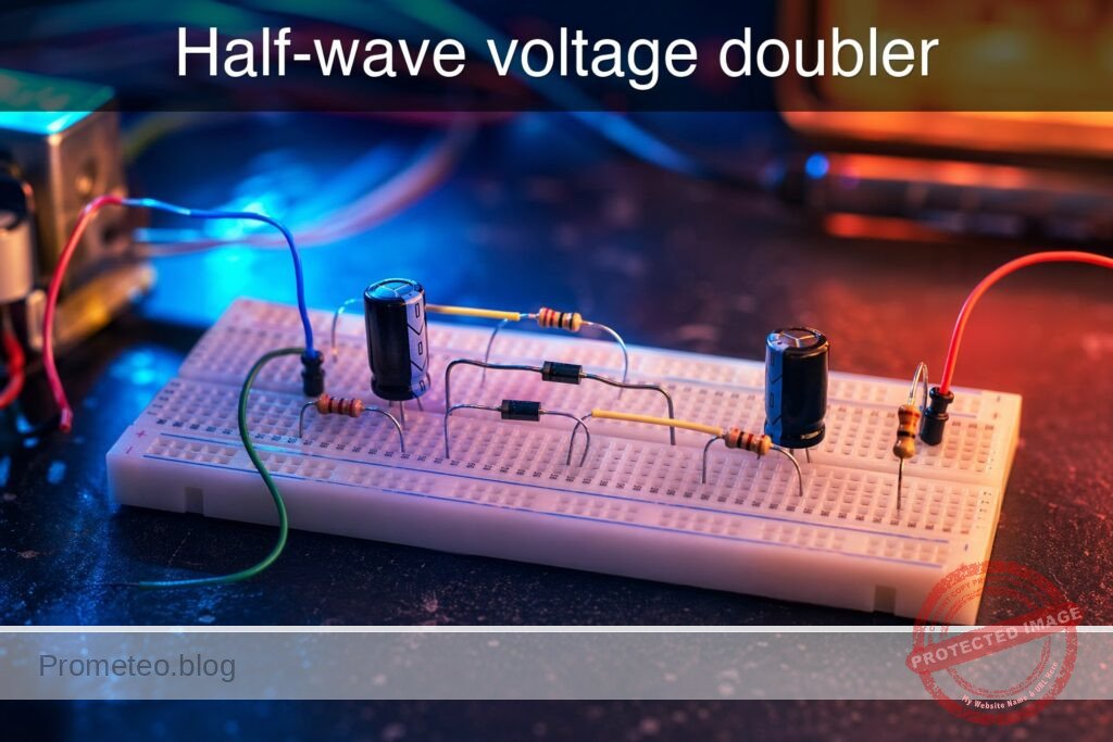
In this practical case, you will build a half-wave voltage doubler (a basic Villard/Greinacher cascade) using two diodes and two capacitors. This circuit rectifies an AC input while simultaneously stepping up the voltage, yielding a DC output roughly twice the peak voltage of the AC source.
Why this circuit is useful in the real world:
* Generating high-voltage bias supplies for components like vacuum tubes, cathode ray tubes, or photomultipliers.
* Providing higher voltage rails for specific operational amplifier stages without requiring a custom, bulky step-up transformer.
* Powering low-current electrostatic devices, ionizers, or Geiger-Müller tubes.
Expected outcome:
* The input signal (V_in_AC) operates as a standard sinusoidal wave.
* The output voltage (V_out_DC) measures approximately 2 × Vpeak of the input signal, minus the forward voltage drops of the two diodes.
* Ripple voltage will be present on the DC output and will noticeably increase when a heavier load (lower resistance) is connected.
Target audience: Intermediate electronics students learning AC-to-DC conversion and fundamental multiplier topologies.
Materials
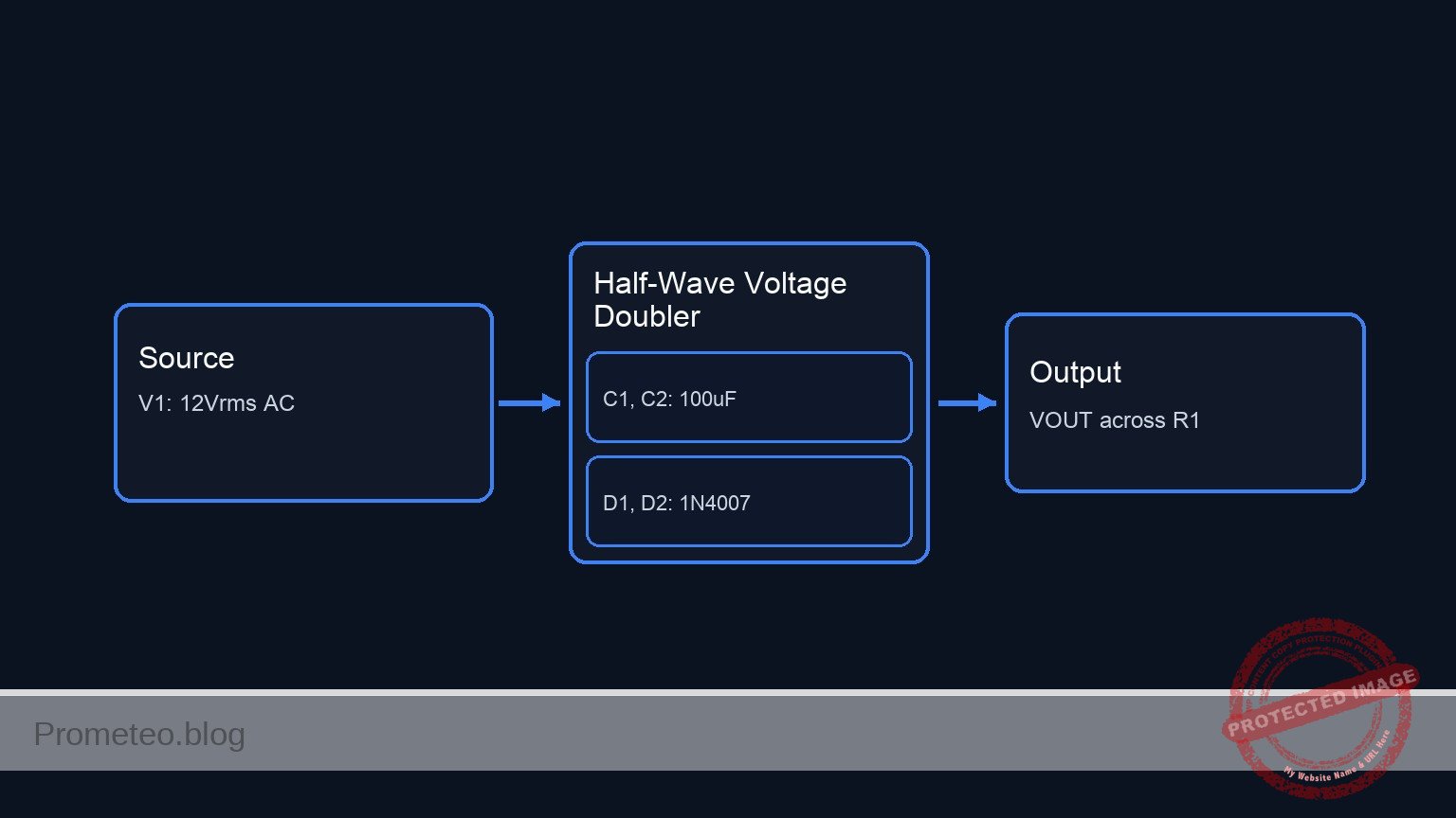
V1: 12 Vrms (approx 17 Vpeak) AC source, 50/60 Hz, function: main AC input signalD1: 1N4007 rectifier diode, function: first clamping stageD2: 1N4007 rectifier diode, function: second peak rectifier stageC1: 100 µF / 50 V electrolytic capacitor, function: AC coupling and intermediate charge storageC2: 100 µF / 50 V electrolytic capacitor, function: output smoothing and final charge storageR1: 10 kΩ resistor, function: light output load to safely discharge capacitors after power off
Wiring guide
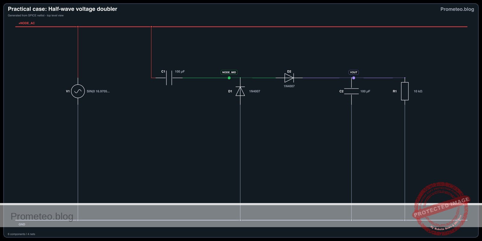
V1: connects between nodeNODE_ACand node0(GND).C1: connects between nodeNODE_AC(negative terminal) and nodeNODE_MID(positive terminal).D1: connects between node0(anode) and nodeNODE_MID(cathode).D2: connects between nodeNODE_MID(anode) and nodeVOUT(cathode).C2: connects between nodeVOUT(positive terminal) and node0(negative terminal).R1: connects between nodeVOUTand node0.
Conceptual block diagram
Schematic
GND
                                                        |
                                                  [ D1: 1N4007 ]
                                                        |
                                                        v
GND --> [ V1: 12Vrms AC ] --(NODE_AC)--> [ C1: 100µF ] --(NODE_MID)--> [ D2: 1N4007 ] --(VOUT)--> [ R1: 10 kΩ ] --> GND
                                                                                            |
                                                                                            +---> [ C2: 100µF ] --> GND
Electrical diagram
Measurements and tests
- Measure the AC Input Peak: Connect an oscilloscope or a multimeter (in AC mode) across node
NODE_ACand node0. A 12 Vrms input should read roughly 17 V peak. - Measure the Intermediate DC Voltage: Place a multimeter (in DC mode) across
C1. You should read approximately Vpeak – 0.7 V (around 16.3 VDC). - Measure the Doubled Output (
V_out_DC): Probe betweenVOUTand0in DC mode. The voltage should be approximately 2 × Vpeak – 1.4 V (around 32.6 VDC). - Observe Output Ripple: Switch the oscilloscope to AC coupling and probe
VOUT. You will observe a ripple wave matching the frequency of the input source (half-wave rectification). - Test Load Dependency: Swap
R1for a 1 kΩ resistor. Notice how the output DC voltage sags and the ripple amplitude increases significantly, proving this topology is best suited for low-current applications.
SPICE netlist and simulation
Reference SPICE Netlist (ngspice) — excerptFull SPICE netlist (ngspice)
* Practical case: Half-wave voltage doubler
.width out=256

* Main AC Input Signal (12 Vrms -> ~16.97 Vpeak, 50 Hz)
V1 NODE_AC 0 SIN(0 16.97056 50)

* AC coupling and intermediate charge storage
* Connected with NODE_MID as positive and NODE_AC as negative terminal
C1 NODE_MID NODE_AC 100u

* First clamping stage rectifier diode
D1 0 NODE_MID 1N4007

* Second peak rectifier stage diode
D2 NODE_MID VOUT 1N4007

* Output smoothing and final charge storage
C2 VOUT 0 100u

* Light output load to safely discharge capacitors
* ... (truncated in public view) ...
Copy this content into a .cir file and run with ngspice.
* Practical case: Half-wave voltage doubler
.width out=256

* Main AC Input Signal (12 Vrms -> ~16.97 Vpeak, 50 Hz)
V1 NODE_AC 0 SIN(0 16.97056 50)

* AC coupling and intermediate charge storage
* Connected with NODE_MID as positive and NODE_AC as negative terminal
C1 NODE_MID NODE_AC 100u

* First clamping stage rectifier diode
D1 0 NODE_MID 1N4007

* Second peak rectifier stage diode
D2 NODE_MID VOUT 1N4007

* Output smoothing and final charge storage
C2 VOUT 0 100u

* Light output load to safely discharge capacitors
R1 VOUT 0 10k

* Diode Model for 1N4007
.model 1N4007 D(IS=7.02767n RS=0.0341512 N=1.80803 EG=1.05743 XTI=5 BV=1000 IBV=5e-08 CJO=1e-11 VJ=0.7 M=0.5 FC=0.5 TT=1e-07)

* Simulation Directives
.print tran V(NODE_AC) V(VOUT) V(NODE_MID)
.tran 100u 500m
.op
.end
* --- GPT review (BOM/Wiring/SPICE) ---
* circuit_ok=true
* simulation_summary: The simulation shows the input AC voltage swinging between approximately -17V and +17V. The intermediate node (NODE_MID) is clamped and shifted, reaching a peak of about 32.6V. The output voltage (VOUT) successfully charges up to approximately 32V, which is nearly double the peak input voltage, confirming the voltage doubler operation.
* overall_comment: The SPICE netlist perfectly matches the BOM and wiring guide. The simulation results clearly demonstrate the expected behavior of a half-wave voltage doubler, with the output voltage reaching approximately twice the peak input voltage. This is an excellent didactic example.
* --------------------------------------
Simulation Results (Transient Analysis)

Show raw data table (5027 rows)
Index   time            v(node_ac)      v(vout)         v(node_mid)
0	0.000000e+00	0.000000e+00	2.565925e-21	-1.89144e-18
1	1.000000e-06	5.331459e-03	5.419582e-10	5.331457e-03
2	2.000000e-06	1.066292e-02	1.097125e-09	1.066291e-02
3	4.000000e-06	2.132583e-02	2.236679e-09	2.132582e-02
4	8.000000e-06	4.265162e-02	4.716739e-09	4.265162e-02
5	1.600000e-05	8.530298e-02	1.109752e-08	8.530296e-02
6	2.994581e-05	1.596525e-01	3.640348e-08	1.596524e-01
7	4.360349e-05	2.324629e-01	1.285942e-07	2.324628e-01
8	5.923389e-05	3.157848e-01	6.926674e-07	3.157841e-01
9	7.569182e-05	4.035098e-01	4.463881e-06	4.035053e-01
10	9.313209e-05	4.964590e-01	3.310357e-05	4.964259e-01
11	1.114841e-04	5.942514e-01	2.714571e-04	5.939798e-01
12	1.306697e-04	6.964642e-01	2.279240e-03	6.941849e-01
13	1.507869e-04	8.036134e-01	1.447578e-02	7.891374e-01
14	1.727320e-04	9.204617e-01	5.134539e-02	8.691153e-01
15	1.929217e-04	1.027924e+00	1.015818e-01	9.263400e-01
16	2.144482e-04	1.142457e+00	1.586780e-01	9.837739e-01
17	2.454175e-04	1.307137e+00	2.410344e-01	1.066092e+00
18	2.845422e-04	1.515006e+00	3.449894e-01	1.169993e+00
19	3.627917e-04	1.930024e+00	5.525467e-01	1.377419e+00
20	4.627917e-04	2.458671e+00	8.169450e-01	1.641599e+00
21	5.627917e-04	2.984892e+00	1.080147e+00	1.904524e+00
22	6.627917e-04	3.508167e+00	1.341889e+00	2.165935e+00
23	7.627917e-04	4.027980e+00	1.601917e+00	2.425574e+00
... (5003 more rows) ...
Reference SPICE netlist (ngspice)
* Practical case: Half-wave voltage doubler
.width out=256

* Main AC Input Signal (12 Vrms -> ~16.97 Vpeak, 50 Hz)
V1 NODE_AC 0 SIN(0 16.97056 50)

* AC coupling and intermediate charge storage
* Connected with NODE_MID as positive and NODE_AC as negative terminal
C1 NODE_MID NODE_AC 100u

* First clamping stage rectifier diode
D1 0 NODE_MID 1N4007

* Second peak rectifier stage diode
D2 NODE_MID VOUT 1N4007

* Output smoothing and final charge storage
C2 VOUT 0 100u

* Light output load to safely discharge capacitors
R1 VOUT 0 10k

* Diode Model for 1N4007
.model 1N4007 D(IS=7.02767n RS=0.0341512 N=1.80803 EG=1.05743 XTI=5 BV=1000 IBV=5e-08 CJO=1e-11 VJ=0.7 M=0.5 FC=0.5 TT=1e-07)

* Simulation Directives
.print tran V(NODE_AC) V(VOUT) V(NODE_MID)
.tran 100u 500m
.op
.end
* --- GPT review (BOM/Wiring/SPICE) ---
* circuit_ok=true
* simulation_summary: The simulation shows the input AC voltage swinging between approximately -17V and +17V. The intermediate node (NODE_MID) is clamped and shifted, reaching a peak of about 32.6V. The output voltage (VOUT) successfully charges up to approximately 32V, which is nearly double the peak input voltage, confirming the voltage doubler operation.
* overall_comment: The SPICE netlist perfectly matches the BOM and wiring guide. The simulation results clearly demonstrate the expected behavior of a half-wave voltage doubler, with the output voltage reaching approximately twice the peak input voltage. This is an excellent didactic example.
* --------------------------------------
Simulation Results (Transient Analysis)
Common mistakes and how to avoid them
- Reversing diode polarity: Installing
D1orD2backward will either clamp the voltage to a negative potential instead of positive, or block the charge from reaching the output entirely. Always check the silver band indicating the cathode. - Incorrect capacitor polarity: Electrolytic capacitors will fail or vent if reverse-biased. Ensure
C1‘s positive terminal faces the diode junction (NODE_MID) andC2‘s positive terminal facesVOUT. - Using capacitors with low voltage ratings:
C2must handle the fully doubled voltage (2 × Vpeak). Using a 25 V capacitor for a 34 V output will cause immediate failure. Always select capacitors rated for at least 2.5 × Vpeak of the AC source.
Troubleshooting
- Symptom: Output voltage is only equal to Vpeak (not doubled).
- Cause:
C1is shorted, orD1is open/damaged. - Fix: Verify
D1‘s continuity using a multimeter diode test and checkC1for internal shorts.
- Cause:
- Symptom: Output voltage (
VOUT) is zero or close to zero.- Cause:
D2is installed backwards (blocking the DC flow), or the load resistorR1is completely shorted/too small, collapsing the multiplier’s charge. - Fix: Verify
D2orientation and ensureR1is at least 10 kΩ for testing.
- Cause:
- Symptom: Loud pop or bulging capacitor upon power-up.
- Cause:
C2voltage rating was exceeded or it was connected with reversed polarity. - Fix: Immediately disconnect power. Replace the damaged capacitor, double-checking correct polarity and a safe voltage rating (e.g., ≥ 50 V).
- Cause:
Possible improvements and extensions
- Add multiplier stages: Cascade additional diodes and capacitors to turn this circuit into a Cockcroft-Walton voltage tripler or quadrupler for even higher DC potentials.
- Build a full-wave voltage doubler: Reconfigure the circuit into a full-wave doubler topology to double the ripple frequency, which reduces the required size of the filter capacitors to maintain a stable output under load.
More Practical Cases on Prometeo.blog
Find this product and/or books on this topic on Amazon
As an Amazon Associate, I earn from qualifying purchases. If you buy through this link, you help keep this project running.
Quick Quiz

Telecommunications Electronics Engineer and Computer Engineer (official degrees in Spain).