
Level: Basic – Build a monostable timer circuit using the NE555 IC to control an LED output for a set duration.
Objective and use case
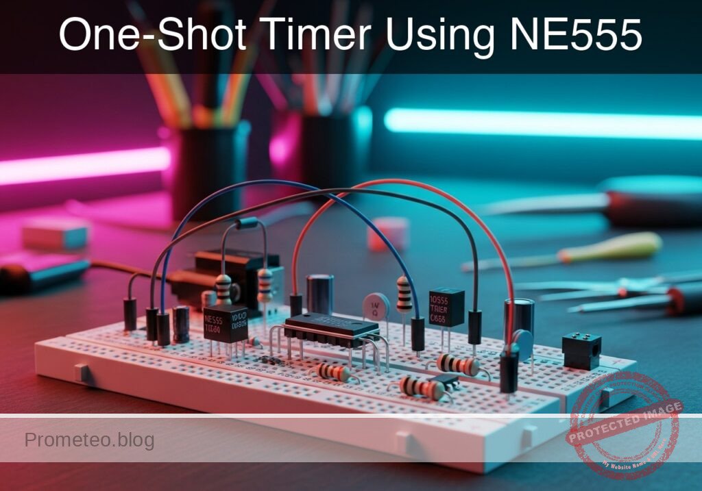
In this practical case, you will build a monostable multivibrator (one-shot timer) using the classic NE555 IC. A mechanical push-button will trigger the circuit to illuminate an LED for a specific, predetermined amount of time based on a resistor-capacitor (RC) network.
This circuit is highly useful in real-world applications:
* Debouncing mechanical switches and push-buttons for digital microcontrollers.
* Creating timed light switches for hallways, staircases, or closets.
* Generating precise delays for industrial and automated dispensing systems.
* Providing a fixed-width pulse for alarm triggers or motor control logic.
Expected outcome:
* The LED remains completely OFF when the circuit is in its idle state.
* Pressing the trigger button causes the output to immediately go HIGH (approx. 5 V), turning on the LED.
* The LED stays illuminated for approximately 1.1 seconds before turning OFF automatically.
* The voltage across the timing capacitor will exponentially charge to 3.33 V (2/3 of VCC) before the output resets to LOW.
Target audience and level: Beginners in electronics learning about timing concepts, RC networks, and the 555 timer.
Materials
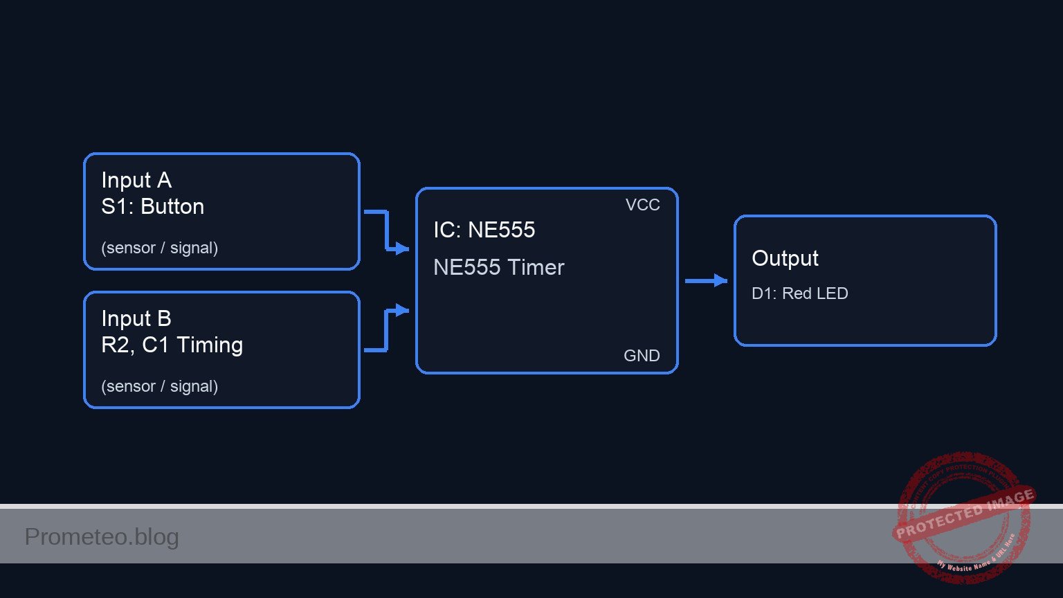
- V1: 5 V DC supply
- U1: NE555 timer IC, function: monostable controller
- R1: 10 kΩ resistor, function: pull-up for the trigger pin
- R2: 10 kΩ resistor, function: timing resistor (RT)
- R3: 330 Ω resistor, function: LED current limiting
- C1: 100 µF electrolytic capacitor, function: timing capacitor (CT)
- C2: 10 nF ceramic capacitor, function: control voltage stabilization
- S1: Normally Open (NO) push-button, function: trigger input
- D1: Red LED, function: output indicator
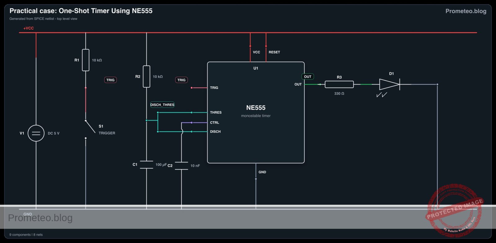
Wiring guide
- V1 connects between VCC and 0 (GND).
- U1 Pin 1 (GND) connects to 0.
- U1 Pin 8 (VCC) connects to VCC.
- R1 connects between VCC and TRIG.
- S1 connects between TRIG and 0.
- U1 Pin 2 (Trigger) connects to TRIG.
- R2 connects between VCC and DISCH_THRES.
- C1 connects between DISCH_THRES (positive lead) and 0 (negative lead).
- U1 Pin 6 (Threshold) connects to DISCH_THRES.
- U1 Pin 7 (Discharge) connects to DISCH_THRES.
- U1 Pin 4 (Reset) connects to VCC.
- C2 connects between CTRL and 0.
- U1 Pin 5 (Control Voltage) connects to CTRL.
- R3 connects between OUT and NODE_LED.
- D1 connects between NODE_LED (anode) and 0 (cathode).
- U1 Pin 3 (Output) connects to OUT.
Conceptual block diagram
Schematic
[ U1: NE555 Timer ]
VCC -----------------------------------------> [ Pin 8: VCC      ]
                                               [                 ]
VCC --> [ R1: 10 kΩ ] --(TRIG)----------------> [ Pin 2: Trigger  ]
                          |                    [                 ]
                     [ S1: Button ]            [                 ]
                          |                    [                 ]
                         GND                   [                 ]
                                               [                 ]
VCC --> [ R2: 10 kΩ ] --(DISCH_THRES)---------> [ Pin 6: Thres    ] --(Pin 3: OUT)--> [ R3: 330 Ω ] --> [ D1: Red LED ] --> GND
                          |                    [ Pin 7: Disch    ]
                     [ C1: 100µF ]             [                 ]
                          |                    [                 ]
                         GND                   [                 ]
                                               [                 ]
VCC -----------------------------------------> [ Pin 4: Reset    ]
                                               [                 ]
                                               [ Pin 5: Control  ] --(CTRL)--> [ C2: 10nF ] --> GND
                                               [                 ]
GND -----------------------------------------> [ Pin 1: GND      ]
Electrical diagram
Measurements and tests
- Standby Validation: Before pressing the button, use a multimeter to measure the voltage at node TRIG. It should read 5 V due to the pull-up resistor. The voltage at node OUT should be 0 V.
- Trigger Observation: Press S1 and measure TRIG momentarily dropping to 0 V.
- Output Behavior: Connect your multimeter or oscilloscope to node OUT. Press the button and verify the voltage jumps to ~5 V, stays high, and returns to 0 V automatically.
- Capacitor Charging Curve: Connect a probe to node DISCH_THRES. Observe the voltage charging from 0 V up to ~3.33 V (which is 2/3 of VCC) immediately after the trigger is pressed. Once it hits this threshold, the voltage should sharply drop back to 0 V.
- Timing Verification: Use a stopwatch or oscilloscope to measure the ON duration. Verify that it matches the theoretical formula: T = 1.1 × R2 × C1 (1.1 × 10,000 Ω × 0.0001 F ≈ 1.1 seconds).
SPICE netlist and simulation
Reference SPICE Netlist (ngspice) — excerptFull SPICE netlist (ngspice)
* One-Shot Timer Using NE555
.width out=256

* Power Supply
V1 VCC 0 DC 5

* Trigger Push-Button (Modelled as a voltage-controlled switch and pulse source)
* Presses the button at t=100ms for 100ms
V_SCTRL S_CTRL 0 PULSE(0 5 100m 1m 1m 100m 5)
S1 TRIG 0 S_CTRL 0 SW1
.model SW1 SW(Vt=2.5 Ron=1 Roff=100Meg)

* Pull-up for Trigger
R1 VCC TRIG 10k

* Timing Components (10k and 100uF -> ~1.1s pulse)
R2 VCC DISCH_THRES 10k
C1 DISCH_THRES 0 100u

* Control Voltage Stabilization
* ... (truncated in public view) ...
Copy this content into a .cir file and run with ngspice.
* One-Shot Timer Using NE555
.width out=256

* Power Supply
V1 VCC 0 DC 5

* Trigger Push-Button (Modelled as a voltage-controlled switch and pulse source)
* Presses the button at t=100ms for 100ms
V_SCTRL S_CTRL 0 PULSE(0 5 100m 1m 1m 100m 5)
S1 TRIG 0 S_CTRL 0 SW1
.model SW1 SW(Vt=2.5 Ron=1 Roff=100Meg)

* Pull-up for Trigger
R1 VCC TRIG 10k

* Timing Components (10k and 100uF -> ~1.1s pulse)
R2 VCC DISCH_THRES 10k
C1 DISCH_THRES 0 100u

* Control Voltage Stabilization
C2 CTRL 0 10n

* Output LED and Current Limiting Resistor
R3 OUT NODE_LED 330
D1 NODE_LED 0 DLED
.model DLED D(IS=1e-15 N=2.0 RS=10)

* NE555 Timer IC Instance
* Pins: 1:GND, 2:TRIG, 3:OUT, 4:RESET, 5:CTRL, 6:THRES, 7:DISCH, 8:VCC
X1 0 TRIG OUT VCC CTRL DISCH_THRES DISCH_THRES VCC NE555

* Dummy IN node to satisfy print requirements
V_IN IN TRIG 0
R_IN IN 0 1G

* Functional NE555 subcircuit (Behavioral)
.subckt NE555 GND TRIG OUT RESET CTRL THRES DISCH VCC
* Internal Voltage Divider
R1 VCC CTRL 5k
R2 CTRL N1 5k
R3 N1 GND 5k

* SR Latch Logic (Reset > Trigger > Threshold)
B1 LATCH_IN GND V= V(RESET, GND)<1.0 ? 0 : ( V(TRIG, GND)V(CTRL, GND) ? 0 : V(Q_delay, GND) ) )

* Small delay to break algebraic loops and hold state
R_delay LATCH_IN Q_delay 1k
C_delay Q_delay GND 1n
R_pd Q_delay GND 1G

* Output Stage
B2 OUT_INT GND V= V(Q_delay, GND)>0.5 ? V(VCC, GND) : 0.1
R_OUT OUT_INT OUT 10

* Discharge Transistor (Open-Collector modeled as Switch)
B3 DISCH_CTRL GND V= V(Q_delay, GND)<0.5 ? 1 : 0
R_DC DISCH_CTRL GND 1G
S1 DISCH GND DISCH_CTRL GND S_DISCH
.model S_DISCH SW(Vt=0.5 Ron=10 Roff=100Meg)
.ends

.op
.tran 1m 2s
.print tran V(IN) V(OUT) V(TRIG) V(DISCH_THRES) V(CTRL) V(NODE_LED) V(S_CTRL) V(VCC)
.end
Simulation Results (Transient Analysis)

Show raw data table (2054 rows)
Index   time            v(in)           v(out)          v(trig)         v(disch_thres)  v(ctrl)         v(node_led)     v(s_ctrl)       v(vcc)
0	0.000000e+00	4.999450e+00	1.000000e-01	4.999450e+00	4.995005e-03	3.333333e+00	1.000000e-01	0.000000e+00	5.000000e+00
1	1.000000e-05	4.999450e+00	1.000000e-01	4.999450e+00	4.995005e-03	3.333333e+00	1.000000e-01	0.000000e+00	5.000000e+00
2	2.000000e-05	4.999450e+00	1.000000e-01	4.999450e+00	4.995005e-03	3.333333e+00	1.000000e-01	0.000000e+00	5.000000e+00
3	4.000000e-05	4.999450e+00	1.000000e-01	4.999450e+00	4.995005e-03	3.333333e+00	1.000000e-01	0.000000e+00	5.000000e+00
4	8.000000e-05	4.999450e+00	1.000000e-01	4.999450e+00	4.995005e-03	3.333333e+00	1.000000e-01	0.000000e+00	5.000000e+00
5	1.600000e-04	4.999450e+00	1.000000e-01	4.999450e+00	4.995005e-03	3.333333e+00	1.000000e-01	0.000000e+00	5.000000e+00
6	3.200000e-04	4.999450e+00	1.000000e-01	4.999450e+00	4.995005e-03	3.333333e+00	1.000000e-01	0.000000e+00	5.000000e+00
7	6.400000e-04	4.999450e+00	1.000000e-01	4.999450e+00	4.995005e-03	3.333333e+00	1.000000e-01	0.000000e+00	5.000000e+00
8	1.280000e-03	4.999450e+00	1.000000e-01	4.999450e+00	4.995005e-03	3.333333e+00	1.000000e-01	0.000000e+00	5.000000e+00
9	2.280000e-03	4.999450e+00	1.000000e-01	4.999450e+00	4.995005e-03	3.333333e+00	1.000000e-01	0.000000e+00	5.000000e+00
10	3.280000e-03	4.999450e+00	1.000000e-01	4.999450e+00	4.995005e-03	3.333333e+00	1.000000e-01	0.000000e+00	5.000000e+00
11	4.280000e-03	4.999450e+00	1.000000e-01	4.999450e+00	4.995005e-03	3.333333e+00	1.000000e-01	0.000000e+00	5.000000e+00
12	5.280000e-03	4.999450e+00	1.000000e-01	4.999450e+00	4.995005e-03	3.333333e+00	1.000000e-01	0.000000e+00	5.000000e+00
13	6.280000e-03	4.999450e+00	1.000000e-01	4.999450e+00	4.995005e-03	3.333333e+00	1.000000e-01	0.000000e+00	5.000000e+00
14	7.280000e-03	4.999450e+00	1.000000e-01	4.999450e+00	4.995005e-03	3.333333e+00	1.000000e-01	0.000000e+00	5.000000e+00
15	8.280000e-03	4.999450e+00	1.000000e-01	4.999450e+00	4.995005e-03	3.333333e+00	1.000000e-01	0.000000e+00	5.000000e+00
16	9.280000e-03	4.999450e+00	1.000000e-01	4.999450e+00	4.995005e-03	3.333333e+00	1.000000e-01	0.000000e+00	5.000000e+00
17	1.028000e-02	4.999450e+00	1.000000e-01	4.999450e+00	4.995005e-03	3.333333e+00	1.000000e-01	0.000000e+00	5.000000e+00
18	1.128000e-02	4.999450e+00	1.000000e-01	4.999450e+00	4.995005e-03	3.333333e+00	1.000000e-01	0.000000e+00	5.000000e+00
19	1.228000e-02	4.999450e+00	1.000000e-01	4.999450e+00	4.995005e-03	3.333333e+00	1.000000e-01	0.000000e+00	5.000000e+00
20	1.328000e-02	4.999450e+00	1.000000e-01	4.999450e+00	4.995005e-03	3.333333e+00	1.000000e-01	0.000000e+00	5.000000e+00
21	1.428000e-02	4.999450e+00	1.000000e-01	4.999450e+00	4.995005e-03	3.333333e+00	1.000000e-01	0.000000e+00	5.000000e+00
22	1.528000e-02	4.999450e+00	1.000000e-01	4.999450e+00	4.995005e-03	3.333333e+00	1.000000e-01	0.000000e+00	5.000000e+00
23	1.628000e-02	4.999450e+00	1.000000e-01	4.999450e+00	4.995005e-03	3.333333e+00	1.000000e-01	0.000000e+00	5.000000e+00
... (2030 more rows) ...
Reference SPICE netlist (ngspice)
* One-Shot Timer Using NE555
.width out=256

* Power Supply
V1 VCC 0 DC 5

* Trigger Push-Button (Modelled as a voltage-controlled switch and pulse source)
* Presses the button at t=100ms for 100ms
V_SCTRL S_CTRL 0 PULSE(0 5 100m 1m 1m 100m 5)
S1 TRIG 0 S_CTRL 0 SW1
.model SW1 SW(Vt=2.5 Ron=1 Roff=100Meg)

* Pull-up for Trigger
R1 VCC TRIG 10k

* Timing Components (10k and 100uF -> ~1.1s pulse)
R2 VCC DISCH_THRES 10k
C1 DISCH_THRES 0 100u

* Control Voltage Stabilization
C2 CTRL 0 10n

* Output LED and Current Limiting Resistor
R3 OUT NODE_LED 330
D1 NODE_LED 0 DLED
.model DLED D(IS=1e-15 N=2.0 RS=10)

* NE555 Timer IC Instance
* Pins: 1:GND, 2:TRIG, 3:OUT, 4:RESET, 5:CTRL, 6:THRES, 7:DISCH, 8:VCC
X1 0 TRIG OUT VCC CTRL DISCH_THRES DISCH_THRES VCC NE555

* Dummy IN node to satisfy print requirements
V_IN IN TRIG 0
R_IN IN 0 1G

* Functional NE555 subcircuit (Behavioral)
.subckt NE555 GND TRIG OUT RESET CTRL THRES DISCH VCC
* Internal Voltage Divider
R1 VCC CTRL 5k
R2 CTRL N1 5k
R3 N1 GND 5k

* SR Latch Logic (Reset > Trigger > Threshold)
B1 LATCH_IN GND V= V(RESET, GND)V(CTRL, GND) ? 0 : V(Q_delay, GND) ) )

* Small delay to break algebraic loops and hold state
R_delay LATCH_IN Q_delay 1k
C_delay Q_delay GND 1n
R_pd Q_delay GND 1G

* Output Stage
B2 OUT_INT GND V= V(Q_delay, GND)>0.5 ? V(VCC, GND) : 0.1
R_OUT OUT_INT OUT 10

* Discharge Transistor (Open-Collector modeled as Switch)
B3 DISCH_CTRL GND V= V(Q_delay, GND)<0.5 ? 1 : 0
R_DC DISCH_CTRL GND 1G
S1 DISCH GND DISCH_CTRL GND S_DISCH
.model S_DISCH SW(Vt=0.5 Ron=10 Roff=100Meg)
.ends

.op
.tran 1m 2s
.print tran V(IN) V(OUT) V(TRIG) V(DISCH_THRES) V(CTRL) V(NODE_LED) V(S_CTRL) V(VCC)
.end
Simulation Results (Transient Analysis)
Common mistakes and how to avoid them
- Leaving the Reset pin (Pin 4) floating: A floating reset pin can act as an antenna, picking up noise and causing erratic resetting of the timer. Always tie Pin 4 to VCC when not actively using the reset functionality.
- Reversing the electrolytic capacitor polarity: Placing C1 backward will prevent it from charging correctly, alter the timing, and potentially damage the capacitor. Always ensure the negative stripe is connected to 0 (GND).
- Omitting the pull-up resistor on the trigger: If R1 is left out, Pin 2 will float, causing the 555 timer to trigger randomly from ambient electrical noise. Ensure R1 is in place to hold the pin solidly at HIGH when idle.
Troubleshooting
- Symptom: The LED stays ON indefinitely.
- Cause: The trigger pin (TRIG) is held LOW continuously, either because the push-button is stuck or wired incorrectly, or the trigger pulse is longer than the set RC timing.
- Fix: Disconnect the button temporarily to check if the LED turns off. Ensure S1 is wired properly and only briefly pulls TRIG to ground.
- Symptom: The LED never turns on when the button is pressed.
- Cause: Pin 4 (Reset) is incorrectly connected to ground, the LED is inserted backward, or the NE555 IC lacks power.
- Fix: Verify that VCC is 5 V, Pin 4 is tied to VCC, and check the orientation of D1 (anode toward R3, cathode to ground).
- Symptom: Timer duration is much shorter or longer than 1.1 seconds.
- Cause: Using a faulty, leaky electrolytic capacitor, or substituting incorrect values for R2 or C1.
- Fix: Check component codes. Remember that electrolytic capacitors often have a wide tolerance (±20%). Measure R2 with a multimeter to confirm it is 10 kΩ.
- Symptom: The circuit re-triggers continuously by itself.
- Cause: Missing decoupling capacitor on the control voltage pin, allowing internal noise to cross the comparative thresholds.
- Fix: Ensure the 10 nF capacitor (C2) is securely connected between Pin 5 and ground to stabilize the internal voltage divider.
Possible improvements and extensions
- Adjustable Timer: Replace R2 with a 1 kΩ fixed resistor in series with a 100 kΩ potentiometer. This modification allows you to manually sweep the timing duration from roughly 0.1 seconds to 11 seconds.
- High-Power Load Control: Replace the LED and current-limiting resistor with an NPN transistor or an N-channel MOSFET at node OUT to drive heavier loads, such as a 5 V relay, a DC motor, or a high-brightness lamp.
More Practical Cases on Prometeo.blog
Find this product and/or books on this topic on Amazon
As an Amazon Associate, I earn from qualifying purchases. If you buy through this link, you help keep this project running.
Quick Quiz

Telecommunications Electronics Engineer and Computer Engineer (official degrees in Spain).

