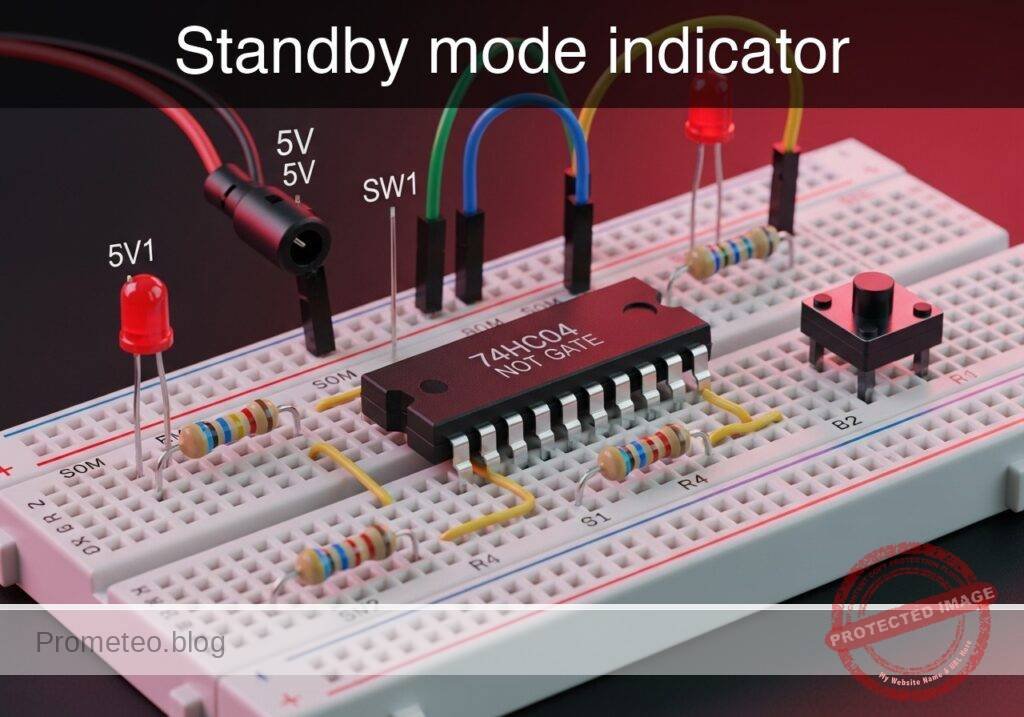
Level: Basic – Understand logical inversion using a NOT gate to activate a standby LED when the main system turns off.
Objective and use case
You will build a digital logic circuit using a 74HC04 NOT gate that monitors a main power switch. When the switch is turned off, the NOT gate logically inverts the signal to activate a «standby» indicator LED.
Why this is useful:
* It perfectly replicates how household appliances (like televisions or microwaves) indicate they are plugged in but currently turned off.
* It provides clear visual feedback in industrial panels when a machine is safe to approach.
* It serves as a foundational example of how to invert control signals for active-low indicators and logic translation.
Expected outcome:
* When the main switch is closed (HIGH logic state, near 5 V), the standby LED remains strictly OFF.
* When the main switch is open (LOW logic state, near 0 V), the standby LED turns ON.
* The circuit accurately demonstrates the inversion of logic states (V_in vs. V_out) through practical voltage measurements.
Target audience and level: Beginners in digital electronics learning basic logic gates.
Materials
- V1: 5 V DC supply, function: main power source
- SW1: SPST switch, function: main system power switch simulator
- R1: 10 kΩ resistor, function: pull-down for VA node
- U1: 74HC04 hex inverter IC, function: logical NOT gate
- R2: 330 Ω resistor, function: LED current limiting
- D1: red LED, function: standby mode indicator
Pin-out of the 74HC04 IC
The 74HC04 is a Hex Inverter IC, meaning it contains six independent NOT gates. We will use the first gate.
| Pin | Name | Logic function | Connection in this case |
|---|---|---|---|
| 1 | 1 A | Data Input | Connects to switch output (VA) |
| 2 | 1Y | Data Output | Connects to LED resistor (VOUT) |
| 7 | GND | Ground | Connects to system ground (0) |
| 14 | VCC | Positive Supply | Connects to positive voltage (VCC) |
(Note: The other input pins [3, 5, 9, 11, 13] should ideally be tied to ground in a permanent circuit to prevent floating inputs and reduce power consumption, but are omitted here for simplicity).
Wiring guide
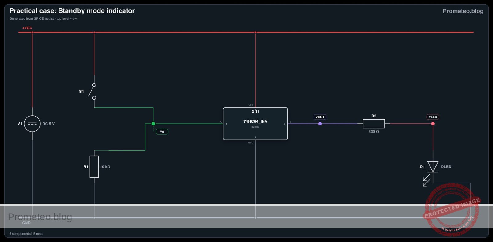
- V1: connects between VCC and 0.
- SW1: connects between VCC and VA.
- R1: connects between VA and 0.
- U1: Pin 14 connects to VCC, Pin 7 connects to 0, Pin 1 (1 A) connects to VA, Pin 2 (1Y) connects to VOUT.
- R2: connects between VOUT and VLED.
- D1: anode connects to VLED, cathode connects to 0.
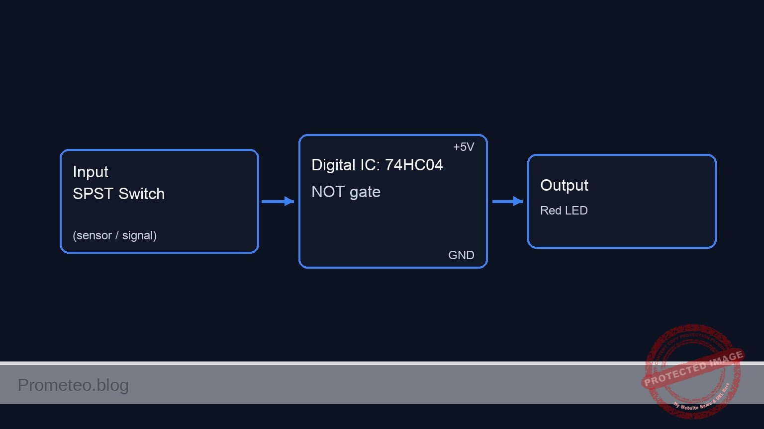
Conceptual block diagram
Schematic
VCC --> [ SW1: SPST Switch ] --(Node VA)--> [ U1: 74HC04 Inverter ] --(VOUT)--> [ R2: 330 Ω Resistor ] --(VLED)--> [ D1: Red LED ] --> GND
                                    |
                                    V
                         [ R1: 10 kΩ Pull-down ]
                                    |
                                    V
                                   GND
Electrical diagram
Truth table
Input (VA) | Output (VOUT) | Standby LED State |
|---|---|---|
| 0 (LOW) | 1 (HIGH) | ON |
| 1 (HIGH) | 0 (LOW) | OFF |
Measurements and tests
- Test the Input Signal (V_in): Connect your multimeter between node VA and ground (0). Open SW1 and verify the voltage is near 0 V. Close SW1 and verify the voltage is near 5 V.
- Test the Inverted Output (V_out): Connect your multimeter between node VOUT and ground (0). Observe the voltage invert: it should be near 5 V when SW1 is open, and near 0 V when SW1 is closed.
- Verify the Logic State: Physically observe D1. Ensure it lights up only when the simulated main system (SW1) is powered down.
SPICE netlist and simulation
Reference SPICE Netlist (ngspice) — excerptFull SPICE netlist (ngspice)
* Practical case: Standby mode indicator
.width out=256

* Power Supply
V1 VCC 0 DC 5

* Switch SW1 (Main system power switch simulator)
* Starts closed (system ON, standby OFF), opens at 50us (system OFF, standby ON)
S1 VCC VA SW_CTRL 0 SWMOD
VSW_CTRL SW_CTRL 0 PULSE(5 0 50u 1u 1u 100u 250u)
.model SWMOD SW(VT=2.5 RON=0.1 ROFF=100MEG)

* Pull-down resistor for switch node VA
R1 VA 0 10k

* U1: 74HC04 Hex Inverter IC
* Pin 1 (1A) = VA, Pin 2 (1Y) = VOUT, Pin 14 = VCC, Pin 7 = 0
XU1 VA VOUT VCC 0 74HC04_INV

* Current limiting resistor for LED
* ... (truncated in public view) ...
Copy this content into a .cir file and run with ngspice.
* Practical case: Standby mode indicator
.width out=256

* Power Supply
V1 VCC 0 DC 5

* Switch SW1 (Main system power switch simulator)
* Starts closed (system ON, standby OFF), opens at 50us (system OFF, standby ON)
S1 VCC VA SW_CTRL 0 SWMOD
VSW_CTRL SW_CTRL 0 PULSE(5 0 50u 1u 1u 100u 250u)
.model SWMOD SW(VT=2.5 RON=0.1 ROFF=100MEG)

* Pull-down resistor for switch node VA
R1 VA 0 10k

* U1: 74HC04 Hex Inverter IC
* Pin 1 (1A) = VA, Pin 2 (1Y) = VOUT, Pin 14 = VCC, Pin 7 = 0
XU1 VA VOUT VCC 0 74HC04_INV

* Current limiting resistor for LED
R2 VOUT VLED 330

* D1: Red LED (Standby mode indicator)
D1 VLED 0 DLED
.model DLED D(IS=1e-15 N=1.8 RS=10)

* Subcircuit for 74HC04 Inverter Gate
.subckt 74HC04_INV A Y VCC GND
B1 Y_int GND V=V(VCC,GND)*0.5*(1-tanh(10*(V(A,GND)-2.5)))
Rin A GND 100Meg
Rout Y_int Y 50
.ends

* Simulation Directives
.tran 1u 300u
.op

* Output Directives (Input and Output nodes listed first)
.print tran V(VA) V(VOUT) V(VLED) V(VCC)

.end
Simulation Results (Transient Analysis)

Show raw data table (340 rows)
Index   time            v(va)           v(vout)         v(vled)         v(vcc)
0	0.000000e+00	4.999950e+00	1.082004e-19	8.223227e-19	5.000000e+00
1	1.000000e-08	4.999950e+00	9.063787e-31	6.888478e-30	5.000000e+00
2	2.000000e-08	4.999950e+00	-9.06379e-31	-6.88848e-30	5.000000e+00
3	4.000000e-08	4.999950e+00	-3.79630e-41	-2.88519e-40	5.000000e+00
4	8.000000e-08	4.999950e+00	1.518521e-41	1.154076e-40	5.000000e+00
5	1.600000e-07	4.999950e+00	1.017634e-51	7.734020e-51	5.000000e+00
6	3.200000e-07	4.999950e+00	-2.54409e-52	-1.93351e-51	5.000000e+00
7	6.400000e-07	4.999950e+00	-2.34426e-62	-1.78164e-61	5.000000e+00
8	1.280000e-06	4.999950e+00	4.262287e-63	3.239338e-62	5.000000e+00
9	2.280000e-06	4.999950e+00	3.983291e-73	3.027301e-72	5.000000e+00
10	3.280000e-06	4.999950e+00	-3.57046e-74	-2.71355e-73	5.000000e+00
11	4.280000e-06	4.999950e+00	-3.93493e-84	-2.99055e-83	5.000000e+00
12	5.280000e-06	4.999950e+00	2.990920e-85	2.273099e-84	5.000000e+00
13	6.280000e-06	4.999950e+00	3.797323e-95	2.885965e-94	5.000000e+00
14	7.280000e-06	4.999950e+00	-2.50545e-96	-1.90414e-95	5.000000e+00
15	8.280000e-06	4.999950e+00	-3.60072e-106	-2.73655e-105	5.000000e+00
16	9.280000e-06	4.999950e+00	2.098779e-107	1.595072e-106	5.000000e+00
17	1.028000e-05	4.999950e+00	3.367893e-117	2.559599e-116	5.000000e+00
18	1.128000e-05	4.999950e+00	-1.75812e-118	-1.33617e-117	5.000000e+00
19	1.228000e-05	4.999950e+00	-3.11579e-128	-2.36800e-127	5.000000e+00
20	1.328000e-05	4.999950e+00	1.472749e-129	1.119289e-128	5.000000e+00
21	1.428000e-05	4.999950e+00	2.856788e-139	2.171159e-138	5.000000e+00
22	1.528000e-05	4.999950e+00	-1.23370e-140	-9.37613e-140	5.000000e+00
23	1.628000e-05	4.999950e+00	-2.59978e-150	-1.97583e-149	5.000000e+00
... (316 more rows) ...
Reference SPICE netlist (ngspice)
* Practical case: Standby mode indicator
.width out=256

* Power Supply
V1 VCC 0 DC 5

* Switch SW1 (Main system power switch simulator)
* Starts closed (system ON, standby OFF), opens at 50us (system OFF, standby ON)
S1 VCC VA SW_CTRL 0 SWMOD
VSW_CTRL SW_CTRL 0 PULSE(5 0 50u 1u 1u 100u 250u)
.model SWMOD SW(VT=2.5 RON=0.1 ROFF=100MEG)

* Pull-down resistor for switch node VA
R1 VA 0 10k

* U1: 74HC04 Hex Inverter IC
* Pin 1 (1A) = VA, Pin 2 (1Y) = VOUT, Pin 14 = VCC, Pin 7 = 0
XU1 VA VOUT VCC 0 74HC04_INV

* Current limiting resistor for LED
R2 VOUT VLED 330

* D1: Red LED (Standby mode indicator)
D1 VLED 0 DLED
.model DLED D(IS=1e-15 N=1.8 RS=10)

* Subcircuit for 74HC04 Inverter Gate
.subckt 74HC04_INV A Y VCC GND
B1 Y_int GND V=V(VCC,GND)*0.5*(1-tanh(10*(V(A,GND)-2.5)))
Rin A GND 100Meg
Rout Y_int Y 50
.ends

* Simulation Directives
.tran 1u 300u
.op

* Output Directives (Input and Output nodes listed first)
.print tran V(VA) V(VOUT) V(VLED) V(VCC)

.end
Simulation Results (Transient Analysis)
Common mistakes and how to avoid them
- Omitting the pull-down resistor (R1): Without R1, opening SW1 leaves the input pin (VA) floating, which can cause the NOT gate to oscillate unpredictably or pick up stray noise. Always secure the LOW state with a pull-down resistor.
- Forgetting IC power pins: It is common to wire the input and output of a logic gate but forget to connect VCC (Pin 14) and GND (Pin 7) on the U1 chip itself. The gate will not function without power.
- Reversing the LED polarity: If D1 is installed backwards (cathode to VLED, anode to 0), it will block current and never light up, even when VOUT correctly outputs 5 V.
Troubleshooting
- Symptom: The standby LED is always OFF.
- Cause: The LED might be backwards, R2 might be too high in value, or the IC is missing power.
- Fix: Check LED orientation (long leg to VLED). Verify U1 pins 14 and 7 are securely connected to VCC and 0.
- Symptom: The standby LED is always ON, regardless of the switch.
- Cause: The switch is not properly connected to VCC, or the switch contacts are faulty, leaving the input permanently pulled LOW by R1.
- Fix: Measure node VA. If it stays at 0 V when the switch is closed, check the wiring from VCC to SW1.
- Symptom: The standby LED flickers when the switch is open.
- Cause: Node VA is floating. R1 is likely disconnected or incorrectly placed.
- Fix: Ensure R1 firmly connects node VA directly to ground (0).
Possible improvements and extensions
- Add a «Main System ON» indicator: Connect a green LED and a 330 Ω resistor directly to node VA to show when the main system is actively running, creating a dual-state visual indicator.
- Drive multiple standby indicators: Use another of the unused NOT gates in the 74HC04 (e.g., input on pin 3 connected to VA, output on pin 4) to drive a secondary standby indicator or a low-power piezo buzzer.
More Practical Cases on Prometeo.blog
Find this product and/or books on this topic on Amazon
As an Amazon Associate, I earn from qualifying purchases. If you buy through this link, you help keep this project running.
Quick Quiz

Telecommunications Electronics Engineer and Computer Engineer (official degrees in Spain).