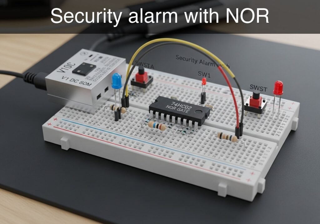
Level: Basic | Objective: Verify the NOR gate truth table using an alarm circuit that activates only when no sensors detect movement.
Objective and use case
We will build a simple security alarm simulator using a 74HC02 NOR gate. In this system, the alarm (an LED) will illuminate only when all connected monitoring sensors (represented by switches) indicate a safe, undisturbed state (Logic 0).
Why it is useful:
* Demonstrates negative logic applications where the absence of inputs is required to trigger an action.
* Provides practical experience with CMOS logic gate behavior and logic-level thresholds.
* Mimics real-world safety interlocks, such as machine guards, where multiple conditions must be false for the system to operate.
* Introduces the essential use of pull-down resistors to ensure stable, predictable logic states.
Expected outcome:
* The output LED will illuminate only when both sensor switches are open (Logic 0, 0 V).
* The output LED will turn off immediately if either or both switches are closed (Logic 1, 5 V).
* Input voltages will measure close to 0 V when switches are open, and near 5 V when closed.
* The output voltage will strictly follow the theoretical truth table of a NOR logic gate.
Target audience: Beginners in digital electronics learning fundamental logic gates and basic control circuits.
Materials
- V1: 5 V DC power supply
- U1: 74HC02 Quad 2-Input NOR Gate
- SW1: SPST switch, function: sensor A input
- SW2: SPST switch, function: sensor B input
- R1: 10 kΩ resistor, function: pull-down for VA
- R2: 10 kΩ resistor, function: pull-down for VB
- R3: 330 Ω resistor, function: LED current limiting
- D1: Red LED, function: alarm active indicator
Pin-out of the IC used
IC Selected: 74HC02
| Pin | Name | Logic function | Connection in this case |
|---|---|---|---|
| 1 | 1Y | Output of Gate 1 | Connects to VOUT |
| 2 | 1 A | Input A of Gate 1 | Connects to VA |
| 3 | 1B | Input B of Gate 1 | Connects to VB |
| 7 | GND | Ground reference | Connects to 0 |
| 14 | VCC | Positive supply voltage | Connects to VCC |
(Note: Pins 4, 5, 6, 8, 9, 10, 11, 12, and 13 belong to the unused gates in the IC package and should ideally have their inputs tied to ground in a permanent design to prevent CMOS floating states).
Wiring guide
- V1: Connects between VCC and 0.
- U1 (Pin 14): Connects to VCC.
- U1 (Pin 7): Connects to 0.
- SW1: Connects between VCC and VA.
- SW2: Connects between VCC and VB.
- R1: Connects between VA and 0.
- R2: Connects between VB and 0.
- U1 (Pin 2): Connects to VA.
- U1 (Pin 3): Connects to VB.
- U1 (Pin 1): Connects to VOUT.
- R3: Connects between VOUT and D1_A.
- D1: Connects between D1_A (anode) and 0 (cathode).
Conceptual block diagram
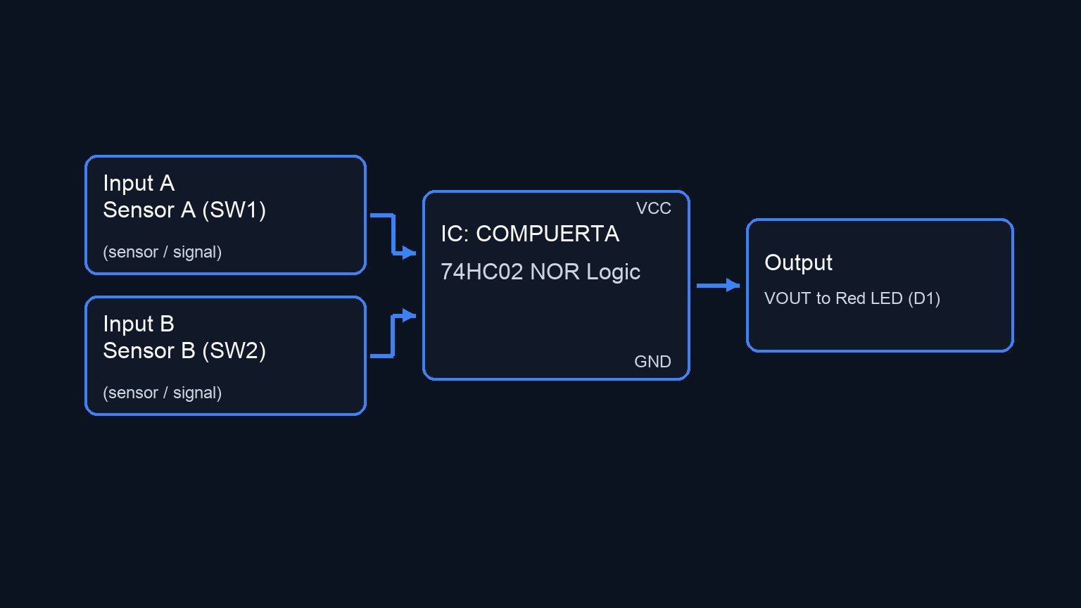
Schematic
VCC   GND
                                           |     |
                                        (Pin14)(Pin7)
VCC --> [ SW1: Sensor A ] --(VA)--> [                   ]
[ VA ] ---> [ R1: 10 kΩ ] ---> GND   [ Pin 2             ]
                                    [ U1: 74HC02 NOR    ] --(Pin 1: VOUT)--> [ R3: 330 Ω ] --> [ D1: Red LED ] --> GND
VCC --> [ SW2: Sensor B ] --(VB)--> [ Pin 3             ]
[ VB ] ---> [ R2: 10 kΩ ] ---> GND   [                   ]
Electrical diagram
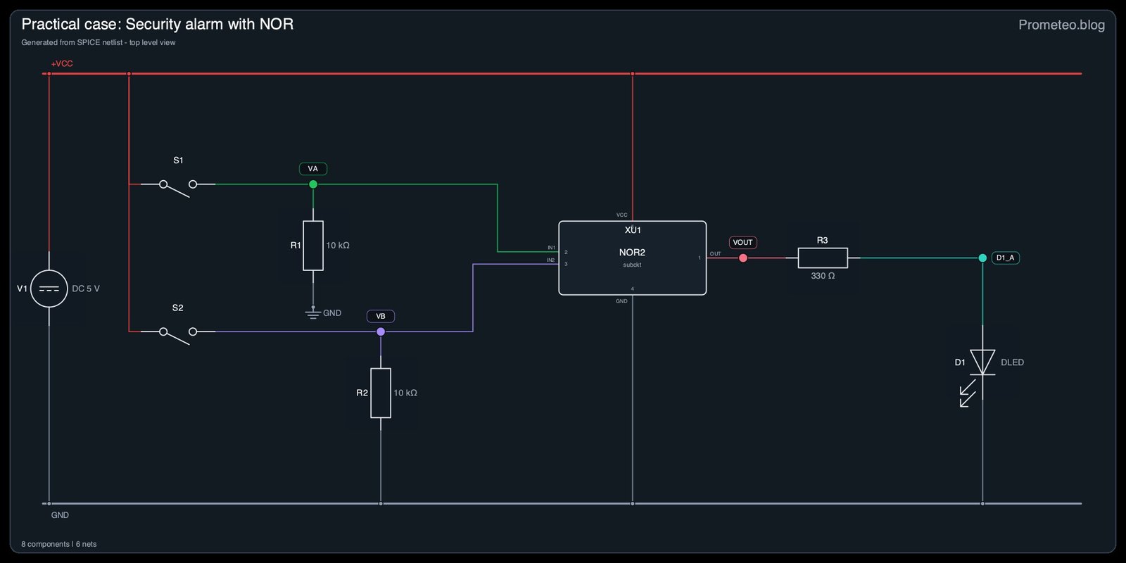
Truth table
Input A (VA) | Input B (VB) | Output Y (VOUT) | Alarm State |
|---|---|---|---|
| 0 | 0 | 1 | LED ON |
| 0 | 1 | 0 | LED OFF |
| 1 | 0 | 0 | LED OFF |
| 1 | 1 | 0 | LED OFF |
Measurements and tests
- Power verification: With the power supply connected, use a multimeter to measure the voltage between nodes VCC and 0. Ensure it is strictly 5 V.
- Idle state test (0, 0): Leave both SW1 and SW2 open. Measure nodes VA and VB with respect to ground; they should be 0 V. Measure VOUT; it should read near 5 V, and the LED should be ON.
- Single sensor test (1, 0 / 0, 1): Close SW1 (leaving SW2 open). Measure VA; it should be 5 V. Measure VOUT; it should immediately drop to 0 V, and the LED should turn OFF. Repeat by opening SW1 and closing SW2.
- Dual sensor test (1, 1): Close both SW1 and SW2. Confirm both VA and VB measure 5 V. Measure VOUT to verify it remains 0 V (LED OFF).
SPICE netlist and simulation
Reference SPICE Netlist (ngspice) — excerptFull SPICE netlist (ngspice)
* Practical case: Security alarm with NOR
.width out=256

* Power supply
V1 VCC 0 DC 5

* Dynamic stimuli for user pressing the switches
VctrlA ctrlA 0 PULSE(0 5 0 1u 1u 50u 100u)
VctrlB ctrlB 0 PULSE(0 5 0 1u 1u 100u 200u)

* Switches representing SW1 and SW2
SW1 VCC VA ctrlA 0 SWMOD
SW2 VCC VB ctrlB 0 SWMOD
.model SWMOD SW(VT=2.5 VH=0.2 RON=1 ROFF=100MEG)

* Pull-down resistors
R1 VA 0 10k
R2 VB 0 10k

* NOR Gate 74HC02 (U1)
* ... (truncated in public view) ...
Copy this content into a .cir file and run with ngspice.
* Practical case: Security alarm with NOR
.width out=256

* Power supply
V1 VCC 0 DC 5

* Dynamic stimuli for user pressing the switches
VctrlA ctrlA 0 PULSE(0 5 0 1u 1u 50u 100u)
VctrlB ctrlB 0 PULSE(0 5 0 1u 1u 100u 200u)

* Switches representing SW1 and SW2
SW1 VCC VA ctrlA 0 SWMOD
SW2 VCC VB ctrlB 0 SWMOD
.model SWMOD SW(VT=2.5 VH=0.2 RON=1 ROFF=100MEG)

* Pull-down resistors
R1 VA 0 10k
R2 VB 0 10k

* NOR Gate 74HC02 (U1)
* Pins: 1=VOUT, 2=VA, 3=VB, 7=0, 14=VCC
XU1 VOUT VA VB 0 VCC NOR2

* Output components
R3 VOUT D1_A 330
D1 D1_A 0 DLED

* Models
.model DLED D(IS=1e-19 N=1.6 RS=10)

* Subcircuits
.subckt NOR2 out in1 in2 gnd vcc
* Robust continuous behavior for NOR logic
B1 out gnd V = V(vcc) * (1 / (1 + exp(20*(V(in1)-2.5)))) * (1 / (1 + exp(20*(V(in2)-2.5))))
.ends

* Analysis
.tran 1u 300u
.print tran V(VA) V(VB) V(VOUT) V(D1_A)
.op
.end
Simulation Results (Transient Analysis)

Show raw data table (417 rows)
Index   time            v(va)           v(vb)           v(vout)         v(d1_a)
0	0.000000e+00	4.999500e-04	4.999500e-04	5.000000e+00	1.719109e+00
1	1.000000e-08	4.999500e-04	4.999500e-04	5.000000e+00	1.719109e+00
2	2.000000e-08	4.999500e-04	4.999500e-04	5.000000e+00	1.719109e+00
3	4.000000e-08	4.999500e-04	4.999500e-04	5.000000e+00	1.719109e+00
4	8.000000e-08	4.999500e-04	4.999500e-04	5.000000e+00	1.719109e+00
5	1.600000e-07	4.999500e-04	4.999500e-04	5.000000e+00	1.719109e+00
6	3.200000e-07	4.999500e-04	4.999500e-04	5.000000e+00	1.719109e+00
7	3.637500e-07	4.999500e-04	4.999500e-04	5.000000e+00	1.719109e+00
8	4.403125e-07	4.999500e-04	4.999500e-04	5.000000e+00	1.719109e+00
9	4.615039e-07	4.999500e-04	4.999500e-04	5.000000e+00	1.719109e+00
10	4.985889e-07	4.999500e-04	4.999500e-04	5.000000e+00	1.719109e+00
11	5.088535e-07	4.999500e-04	4.999500e-04	5.000000e+00	1.719109e+00
12	5.268165e-07	4.999500e-04	4.999500e-04	5.000000e+00	1.719109e+00
13	5.467041e-07	4.999500e+00	4.999500e+00	1.897609e-43	8.840581e-30
14	5.864794e-07	4.999500e+00	4.999500e+00	1.897609e-43	3.298742e-17
15	6.660299e-07	4.999500e+00	4.999500e+00	1.897609e-43	7.028545e-34
16	8.251311e-07	4.999500e+00	4.999500e+00	1.897609e-43	7.526757e-34
17	1.000000e-06	4.999500e+00	4.999500e+00	1.897609e-43	1.897616e-43
18	1.031820e-06	4.999500e+00	4.999500e+00	1.897609e-43	1.897608e-43
19	1.095461e-06	4.999500e+00	4.999500e+00	1.897609e-43	1.897609e-43
20	1.222742e-06	4.999500e+00	4.999500e+00	1.897609e-43	1.897609e-43
21	1.477303e-06	4.999500e+00	4.999500e+00	1.897609e-43	1.897609e-43
22	1.986427e-06	4.999500e+00	4.999500e+00	1.897609e-43	1.897609e-43
23	2.986427e-06	4.999500e+00	4.999500e+00	1.897609e-43	1.897609e-43
... (393 more rows) ...
Reference SPICE netlist (ngspice)
* Practical case: Security alarm with NOR
.width out=256

* Power supply
V1 VCC 0 DC 5

* Dynamic stimuli for user pressing the switches
VctrlA ctrlA 0 PULSE(0 5 0 1u 1u 50u 100u)
VctrlB ctrlB 0 PULSE(0 5 0 1u 1u 100u 200u)

* Switches representing SW1 and SW2
SW1 VCC VA ctrlA 0 SWMOD
SW2 VCC VB ctrlB 0 SWMOD
.model SWMOD SW(VT=2.5 VH=0.2 RON=1 ROFF=100MEG)

* Pull-down resistors
R1 VA 0 10k
R2 VB 0 10k

* NOR Gate 74HC02 (U1)
* Pins: 1=VOUT, 2=VA, 3=VB, 7=0, 14=VCC
XU1 VOUT VA VB 0 VCC NOR2

* Output components
R3 VOUT D1_A 330
D1 D1_A 0 DLED

* Models
.model DLED D(IS=1e-19 N=1.6 RS=10)

* Subcircuits
.subckt NOR2 out in1 in2 gnd vcc
* Robust continuous behavior for NOR logic
B1 out gnd V = V(vcc) * (1 / (1 + exp(20*(V(in1)-2.5)))) * (1 / (1 + exp(20*(V(in2)-2.5))))
.ends

* Analysis
.tran 1u 300u
.print tran V(VA) V(VB) V(VOUT) V(D1_A)
.op
.end
Simulation Results (Transient Analysis)
Common mistakes and how to avoid them
- Misinterpreting the 74HC02 pinout: Unlike standard AND/OR gates (where pins 1 and 2 are inputs and 3 is the output), the 74HC02 has its output on Pin 1, and inputs on Pins 2 and 3. Wiring it like a 74HC08 will result in short circuits and component failure.
- Floating inputs (Missing pull-down resistors): Omitting R1 or R2 leaves the CMOS inputs floating when the switches are open. This causes the output to oscillate or randomly toggle based on environmental electromagnetic noise. Always ensure your inputs have a defined path to ground.
- Reversing LED polarity: Connecting the LED backwards (anode to ground) will prevent it from lighting up, even if the gate outputs a correct 5 V Logic 1 state.
Troubleshooting
- Symptom: LED is always OFF, even when both switches are open.
- Cause: Floating inputs acting as logic HIGH, or an incorrect wiring to Pin 1 (Output).
- Fix: Verify R1 and R2 are properly connected between the input nodes (VA, VB) and ground (0). Double-check that the LED is connected to Pin 1, not Pin 3.
- Symptom: IC becomes excessively hot to the touch.
- Cause: Power pins (VCC and 0) are reversed, or an output pin is directly shorted to ground or VCC.
- Fix: Instantly disconnect power. Verify Pin 14 goes strictly to VCC and Pin 7 goes strictly to 0.
- Symptom: The alarm triggers (LED turns ON) when any switch is closed, rather than when they are open.
- Cause: Using an OR gate (74HC32) instead of a NOR gate (74HC02), or using pull-up resistors instead of pull-downs.
- Fix: Check the markings on the IC package to ensure it is a 74HC02, and verify R1 and R2 are wired to ground (0).
Possible improvements and extensions
- Audible Alarm Integration: Replace or parallel the indicator LED with a low-current 5 V active piezo buzzer to create a more realistic security warning system.
- System Expansion: Cascade multiple NOR gates or combine them with OR gates to expand the system from a 2-sensor alarm to a 4-sensor setup, keeping the rule that no sensors must be active to trigger the output.
More Practical Cases on Prometeo.blog
Find this product and/or books on this topic on Amazon
As an Amazon Associate, I earn from qualifying purchases. If you buy through this link, you help keep this project running.
Quick Quiz

Telecommunications Electronics Engineer and Computer Engineer (official degrees in Spain).