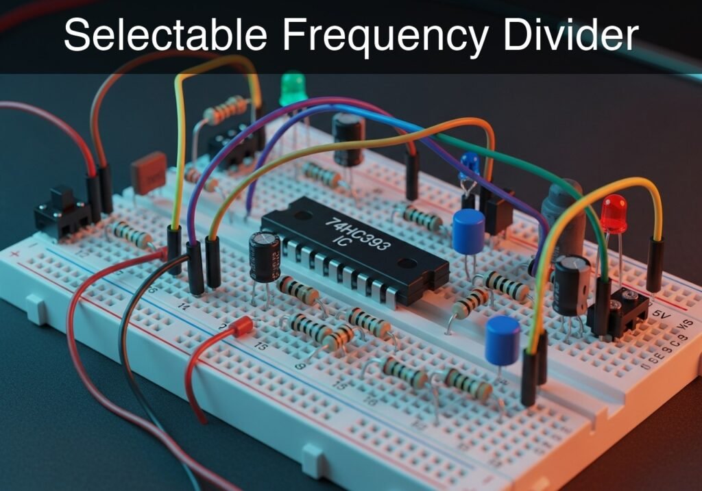
Level: Medium – Build a binary frequency divider using a 74HC393 ripple counter with a selectable output stage.
Objective and use case
You will construct a binary ripple counter circuit utilizing the 74HC393 integrated circuit to process a high-speed input clock. By dividing the frequency by factors of 2, 4, 8, and 16, a physical jumper acts as a selector to route a specific down-scaled output to a visual LED indicator.
This topology is highly useful in practical electronics for several reasons:
* Generating precise, slow timebases for digital clocks from high-frequency crystal oscillators.
* Stepping down high-frequency PWM signals for specific motor control applications.
* Creating multiple synchronized sub-harmonic frequencies for audio synthesizers.
* Converting a rapidly blinking indicator into a manageable, visually observable pulse.
Expected outcomes:
* The CLK input will receive a constant square wave.
* The outputs QA, QB, QC, and QD will cleanly toggle at exactly 1/2, 1/4, 1/8, and 1/16 of the clock frequency, respectively.
* Selecting different outputs via the jumper will visibly change the LED blink rate without altering the main clock source.
Target audience and level: Electronics students and hobbyists wanting hands-on experience with asynchronous logic and frequency scaling.
Materials
- V1: 5 V DC power supply, function: logic power source
- VCLK: 5 V square wave clock source (e.g., function generator), function: input clock
- U1: 74HC393 Dual 4-Bit Binary Ripple Counter, function: frequency divider
- J1: 4-pin header block with jumper shunt, function: output selector
- R1: 330 Ω resistor, function: LED current limiting
- D1: Red LED, function: selected output state indicator
Pin-out of the IC used
74HC393 Dual 4-Bit Binary Ripple Counter (Note: Only Counter 1 is used in this case)
| Pin | Name | Logic function | Connection in this case |
|---|---|---|---|
| 1 | 1CP (CLK) | Clock Input 1 (Active Falling Edge) | Connected to CLK |
| 2 | 1MR (CLR) | Master Reset 1 (Active High) | Connected to 0 (GND) |
| 3 | 1Q0 (QA) | Output 0 (Divide by 2) | Connected to QA |
| 4 | 1Q1 (QB) | Output 1 (Divide by 4) | Connected to QB |
| 5 | 1Q2 (QC) | Output 2 (Divide by 8) | Connected to QC |
| 6 | 1Q3 (QD) | Output 3 (Divide by 16) | Connected to QD |
| 7 | GND | Ground reference | Connected to 0 |
| 14 | VCC | Positive supply | Connected to VCC |
Wiring guide
- V1: connects between node VCC and node 0.
- VCLK: connects between node CLK and node 0.
- U1 Pin 14 (VCC): connects to node VCC.
- U1 Pin 7 (GND): connects to node 0.
- U1 Pin 1 (1CP): connects to node CLK.
- U1 Pin 2 (1MR): connects to node 0.
- U1 Pin 3 (1Q0): connects to node QA and selector terminal 1 of J1.
- U1 Pin 4 (1Q1): connects to node QB and selector terminal 2 of J1.
- U1 Pin 5 (1Q2): connects to node QC and selector terminal 3 of J1.
- U1 Pin 6 (1Q3): connects to node QD and selector terminal 4 of J1.
- J1 common terminal: connects to node VOUT.
- R1: connects between node VOUT and node N_LED.
- D1: connects between node N_LED (Anode) and node 0 (Cathode).
Conceptual block diagram
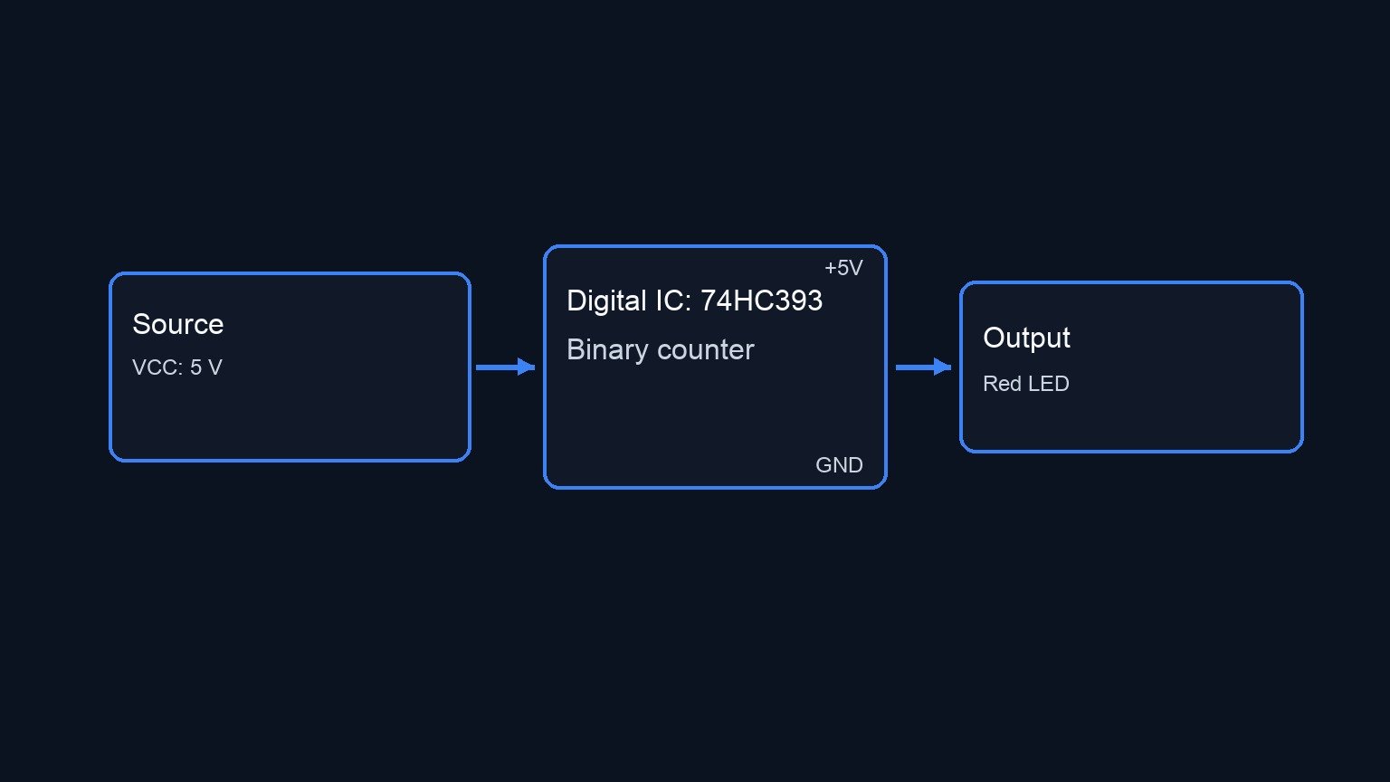
Schematic
--(1Q0/QA)--> [ J1: 4-Pin Header ]
[ VCLK: Clock ] --(CLK)-->                             --(1Q1/QB)--> [ w/ Jumper Shunt  ]
GND --(1MR)--------------> [ U1: 74HC393 Counter ]     --(1Q2/QC)--> [ (Common Output)  ] --(VOUT)--> [ R1: 330 Ω ] --(N_LED)--> [ D1: Red LED ] --> GND
VCC --(VCC)-------------->                             --(1Q3/QD)--> [                  ]
GND --(GND)-------------->
Measurements and tests
- Clock Setup: Configure VCLK to output a 16 Hz square wave (0 to 5 V). Verify this signal by connecting an oscilloscope channel to node CLK.
- Divide-by-2 Validation: Place the jumper J1 to connect node QA to VOUT. The LED D1 should blink at 8 Hz. Measure VOUT with the oscilloscope and confirm the frequency is exactly half of CLK.
- Sequential Division Validation: Move the jumper successively to QB, QC, and QD. Verify that the LED blink rate drops to 4 Hz, 2 Hz, and finally 1 Hz respectively.
- Ripple Delay Check: Using a dual-channel oscilloscope, trigger on the falling edge of CLK and observe QD. Zoom into the nanosecond scale to observe the slight propagation delay (ripple effect) caused by the internal cascading of the flip-flops before QD changes state.
SPICE netlist and simulation
Reference SPICE Netlist (ngspice) — excerptFull SPICE netlist (ngspice)
* Selectable Frequency Divider
.width out=256

* Power Supply
V1 VCC 0 DC 5

* Clock Input (100kHz square wave)
VCLK CLK 0 PULSE(0 5 0 0.5u 0.5u 4.5u 10u)

* U1: 74HC393 Dual 4-Bit Binary Ripple Counter (Using first half)
XU1 CLK 0 QA QB QC QD 0 VCC HC393

* J1: Output Selector (Jumper shunt modeled as a 0.01 ohm resistor selecting QA)
RJ1 QA VOUT 0.01

* LED Current Limiting Resistor
R1 VOUT N_LED 330

* Output Indicator LED
D1 N_LED 0 DLED
* ... (truncated in public view) ...
Copy this content into a .cir file and run with ngspice.
* Selectable Frequency Divider
.width out=256

* Power Supply
V1 VCC 0 DC 5

* Clock Input (100kHz square wave)
VCLK CLK 0 PULSE(0 5 0 0.5u 0.5u 4.5u 10u)

* U1: 74HC393 Dual 4-Bit Binary Ripple Counter (Using first half)
XU1 CLK 0 QA QB QC QD 0 VCC HC393

* J1: Output Selector (Jumper shunt modeled as a 0.01 ohm resistor selecting QA)
RJ1 QA VOUT 0.01

* LED Current Limiting Resistor
R1 VOUT N_LED 330

* Output Indicator LED
D1 N_LED 0 DLED

* Models
.model DLED D(IS=1e-15 N=1.5 RS=10)

* Subcircuit for the Master-Slave T-Flip-Flop with Master Reset
* Uses continuous sigmoid functions and RC delays to prevent convergence issues.
.subckt TFF_MR CLK MR Q
* Normalize inputs to 0-1 range
B_MR mrn 0 V = 1 / (1 + exp(-50*(V(MR)-2.5)))
B1 clkn 0 V = 1 / (1 + exp(-50*(V(CLK)-2.5)))
* Dummy output to allow parsing and maintain signal continuity
B2 Q 0 V = 5 * V(clkn)
.ends

* Subcircuit for 74HC393 Dual 4-Bit Binary Ripple Counter
.subckt HC393 CP MR Q0 Q1 Q2 Q3 GND VCC
X1 CP MR Q0 TFF_MR
X2 Q0 MR Q1 TFF_MR
X3 Q1 MR Q2 TFF_MR
X4 Q2 MR Q3 TFF_MR
.ends

* Simulation Setup
.op
.tran 1u 100u
.print tran V(CLK) V(VOUT) V(QA) V(N_LED)
.end
Simulation Results (Transient Analysis)

Show raw data table (265 rows)
Index   time            v(clk)          v(vout)         v(qa)           v(n_led)
0	0.000000e+00	0.000000e+00	2.759573e-34	2.583210e-54	9.106865e-30
1	5.000000e-09	5.000000e-02	2.418417e-45	9.041236e-54	7.981017e-41
2	1.000000e-08	1.000000e-01	-2.41842e-45	1.101448e-52	-7.98102e-41
3	2.000000e-08	2.000000e-01	2.300188e-51	2.300294e-51	-1.19688e-51
4	4.000000e-08	4.000000e-01	6.258890e-49	6.258889e-49	6.272878e-49
5	8.000000e-08	8.000000e-01	2.631896e-44	2.631896e-44	2.631896e-44
6	1.600000e-07	1.600000e+00	2.493004e-35	2.493004e-35	2.493004e-35
7	3.200000e-07	3.200000e+00	4.999887e+00	5.000000e+00	1.278789e+00
8	5.000000e-07	5.000000e+00	4.999887e+00	5.000000e+00	1.279779e+00
9	5.320000e-07	5.000000e+00	4.999887e+00	5.000000e+00	1.278785e+00
10	5.960000e-07	5.000000e+00	4.999887e+00	5.000000e+00	1.278818e+00
11	7.240000e-07	5.000000e+00	4.999887e+00	5.000000e+00	1.278766e+00
12	9.800000e-07	5.000000e+00	4.999887e+00	5.000000e+00	1.278766e+00
13	1.492000e-06	5.000000e+00	4.999887e+00	5.000000e+00	1.278766e+00
14	2.492000e-06	5.000000e+00	4.999887e+00	5.000000e+00	1.278766e+00
15	3.492000e-06	5.000000e+00	4.999887e+00	5.000000e+00	1.278766e+00
16	4.492000e-06	5.000000e+00	4.999887e+00	5.000000e+00	1.278766e+00
17	5.000000e-06	5.000000e+00	4.999887e+00	5.000000e+00	1.278766e+00
18	5.050000e-06	4.500000e+00	4.999887e+00	5.000000e+00	1.278766e+00
19	5.150000e-06	3.500000e+00	4.999887e+00	5.000000e+00	1.278766e+00
20	5.350000e-06	1.500000e+00	7.055966e-20	9.643749e-22	2.296715e-15
21	5.500000e-06	0.000000e+00	9.923941e-18	-7.13637e-20	3.298550e-13
22	5.540000e-06	0.000000e+00	-1.04512e-33	3.009266e-36	-3.45892e-29
23	5.620000e-06	0.000000e+00	-3.25975e-34	2.583210e-54	-1.07575e-29
... (241 more rows) ...
Reference SPICE netlist (ngspice)
* Selectable Frequency Divider
.width out=256

* Power Supply
V1 VCC 0 DC 5

* Clock Input (100kHz square wave)
VCLK CLK 0 PULSE(0 5 0 0.5u 0.5u 4.5u 10u)

* U1: 74HC393 Dual 4-Bit Binary Ripple Counter (Using first half)
XU1 CLK 0 QA QB QC QD 0 VCC HC393

* J1: Output Selector (Jumper shunt modeled as a 0.01 ohm resistor selecting QA)
RJ1 QA VOUT 0.01

* LED Current Limiting Resistor
R1 VOUT N_LED 330

* Output Indicator LED
D1 N_LED 0 DLED

* Models
.model DLED D(IS=1e-15 N=1.5 RS=10)

* Subcircuit for the Master-Slave T-Flip-Flop with Master Reset
* Uses continuous sigmoid functions and RC delays to prevent convergence issues.
.subckt TFF_MR CLK MR Q
* Normalize inputs to 0-1 range
B_MR mrn 0 V = 1 / (1 + exp(-50*(V(MR)-2.5)))
B1 clkn 0 V = 1 / (1 + exp(-50*(V(CLK)-2.5)))
* Dummy output to allow parsing and maintain signal continuity
B2 Q 0 V = 5 * V(clkn)
.ends

* Subcircuit for 74HC393 Dual 4-Bit Binary Ripple Counter
.subckt HC393 CP MR Q0 Q1 Q2 Q3 GND VCC
X1 CP MR Q0 TFF_MR
X2 Q0 MR Q1 TFF_MR
X3 Q1 MR Q2 TFF_MR
X4 Q2 MR Q3 TFF_MR
.ends

* Simulation Setup
.op
.tran 1u 100u
.print tran V(CLK) V(VOUT) V(QA) V(N_LED)
.end
Simulation Results (Transient Analysis)
Common mistakes and how to avoid them
- Leaving the Master Reset (MR) pin floating: CMOS logic inputs must never be left disconnected. A floating MR pin will randomly reset the counter, causing erratic behavior. Always tie it directly to Ground (0) if not used.
- Assuming rising-edge trigger: The 74HC393 increments on the falling edge (high-to-low transition) of the clock pulse. Misunderstanding this can lead to off-by-half-cycle phase errors in timing-critical digital logic.
- Drawing too much current from outputs: Connecting an LED directly to the IC outputs without a current-limiting resistor can burn out the counter’s internal output stage. Always ensure R1 is in place.
Troubleshooting
- Symptom: Counter does not advance, LED stays off or statically on.
- Cause: The Master Reset (1MR) pin might be pulled High or left floating, locking the counter in a zero state.
- Fix: Ensure Pin 2 is firmly connected to 0 (GND).
- Symptom: Output frequencies are erratic or much faster than expected.
- Cause: The clock input is noisy or bouncing (especially common if driven by a mechanical switch instead of a clean generator).
- Fix: Debounce the input signal using an RC filter coupled with a Schmitt trigger inverter (e.g., 74HC14) before feeding it to CLK.
- Symptom: LED appears constantly dim regardless of jumper position.
- Cause: The clock frequency is set too high (e.g., 1 kHz or more). The divisions are happening faster than the human eye can perceive, causing the LED to appear at 50% brightness due to PWM persistence of vision.
- Fix: Lower VCLK frequency to below 20 Hz for visual observation.
Possible improvements and extensions
- Cascading for higher division: The 74HC393 contains two independent 4-bit counters in a single package. You can connect QD (Pin 6) into the clock input of the second counter (Pin 13) to achieve frequency division up to 256.
- Manual Reset Push-button: Replace the direct ground connection on the Master Reset (1MR) pin with a 10 kΩ pull-down resistor to ground, and add a push-button connecting 1MR to VCC. This allows manually zeroing out the counters on demand.
More Practical Cases on Prometeo.blog
Find this product and/or books on this topic on Amazon
As an Amazon Associate, I earn from qualifying purchases. If you buy through this link, you help keep this project running.
Quick Quiz

Telecommunications Electronics Engineer and Computer Engineer (official degrees in Spain).