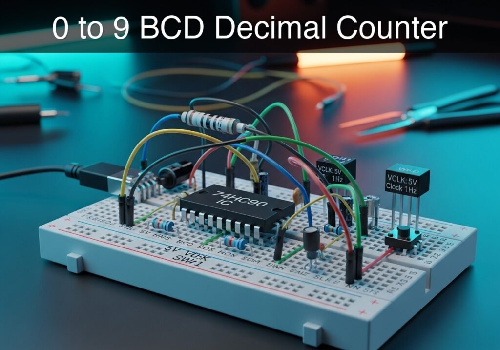
Level: Medium | Build a 0-9 BCD counter using the 74HC90 IC to visualize binary progression via LEDs.
Objective and use case
You will construct a decade (0-9) Binary Coded Decimal (BCD) counter using a 74HC90 IC, driven by a clock pulse source, and terminating in four LEDs to display the binary state.
This circuit is highly useful in real-world applications for:
* Building fundamental digital clock circuits (seconds and minutes counters).
* Event counting systems on manufacturing lines.
* Understanding logic state machines and frequency dividers (divide-by-10).
* Creating foundational timing circuits without the need for microcontrollers.
Expected outcome:
* The circuit will automatically count from 0000 (decimal 0) to 1001 (decimal 9) in binary.
* A transient validation will show the CLK signal alongside the state of QA, QB, QC, and QD.
* Pressing the manual reset button will immediately pull the RST node HIGH and force the outputs to 0000.
* The LEDs will visually blink according to their respective binary significance (QA toggling fastest, QD toggling slowest).
Target audience and level: Intermediate electronics students learning sequential logic and counters.
Materials
- V1: 5 V DC supply
- VCLK: 5 V square wave clock source (1 Hz), function: clock input
- U1: 74HC90 decade counter IC
- SW1: Push-button (Normally Open), function: manual reset trigger
- R1: 10 kΩ resistor, function: pull-down for the RST node
- R2: 330 Ω resistor, function: LED current limiting for QA
- R3: 330 Ω resistor, function: LED current limiting for QB
- R4: 330 Ω resistor, function: LED current limiting for QC
- R5: 330 Ω resistor, function: LED current limiting for QD
- D1: Red LED, function: QA indicator (LSB)
- D2: Red LED, function: QB indicator
- D3: Red LED, function: QC indicator
- D4: Red LED, function: QD indicator (MSB)
Pin-out of the IC used
74HC90 (Decade Counter)
| Pin | Name | Logic function | Connection in this case |
|---|---|---|---|
| 1 | CKB | Clock Input B | Connected to QA (Internal counter cascade) |
| 2 | MR1 | Master Reset 1 | Connected to RST |
| 3 | MR2 | Master Reset 2 | Connected to RST |
| 4 | NC | No Connection | Leave unconnected |
| 5 | VCC | Positive Supply | Connected to VCC |
| 6 | MS1 | Master Set 1 (to 9) | Connected to 0 (GND) |
| 7 | MS2 | Master Set 2 (to 9) | Connected to 0 (GND) |
| 8 | QC | Output C | Connected to QC |
| 9 | QB | Output B | Connected to QB |
| 10 | GND | Ground | Connected to 0 (GND) |
| 11 | QD | Output D (MSB) | Connected to QD |
| 12 | QA | Output A (LSB) | Connected to QA |
| 13 | NC | No Connection | Leave unconnected |
| 14 | CKA | Clock Input A | Connected to CLK |
Wiring guide
- V1: connects between VCC and 0 (GND).
- VCLK: connects between CLK and 0.
- SW1: connects between VCC and RST.
- R1: connects between RST and 0.
- U1 Pin 5 (VCC): connects to VCC.
- U1 Pin 10 (GND): connects to 0.
- U1 Pin 14 (CKA): connects to CLK.
- U1 Pin 1 (CKB): connects to QA.
- U1 Pin 2 (MR1): connects to RST.
- U1 Pin 3 (MR2): connects to RST.
- U1 Pin 6 (MS1): connects to 0.
- U1 Pin 7 (MS2): connects to 0.
- U1 Pin 12 (QA): connects to QA.
- U1 Pin 9 (QB): connects to QB.
- U1 Pin 8 (QC): connects to QC.
- U1 Pin 11 (QD): connects to QD.
- R2: connects between QA and node N_D1.
- D1 (QA LED): connects between N_D1 (anode) and 0 (cathode).
- R3: connects between QB and node N_D2.
- D2 (QB LED): connects between N_D2 (anode) and 0 (cathode).
- R4: connects between QC and node N_D3.
- D3 (QC LED): connects between N_D3 (anode) and 0 (cathode).
- R5: connects between QD and node N_D4.
- D4 (QD LED): connects between N_D4 (anode) and 0 (cathode).
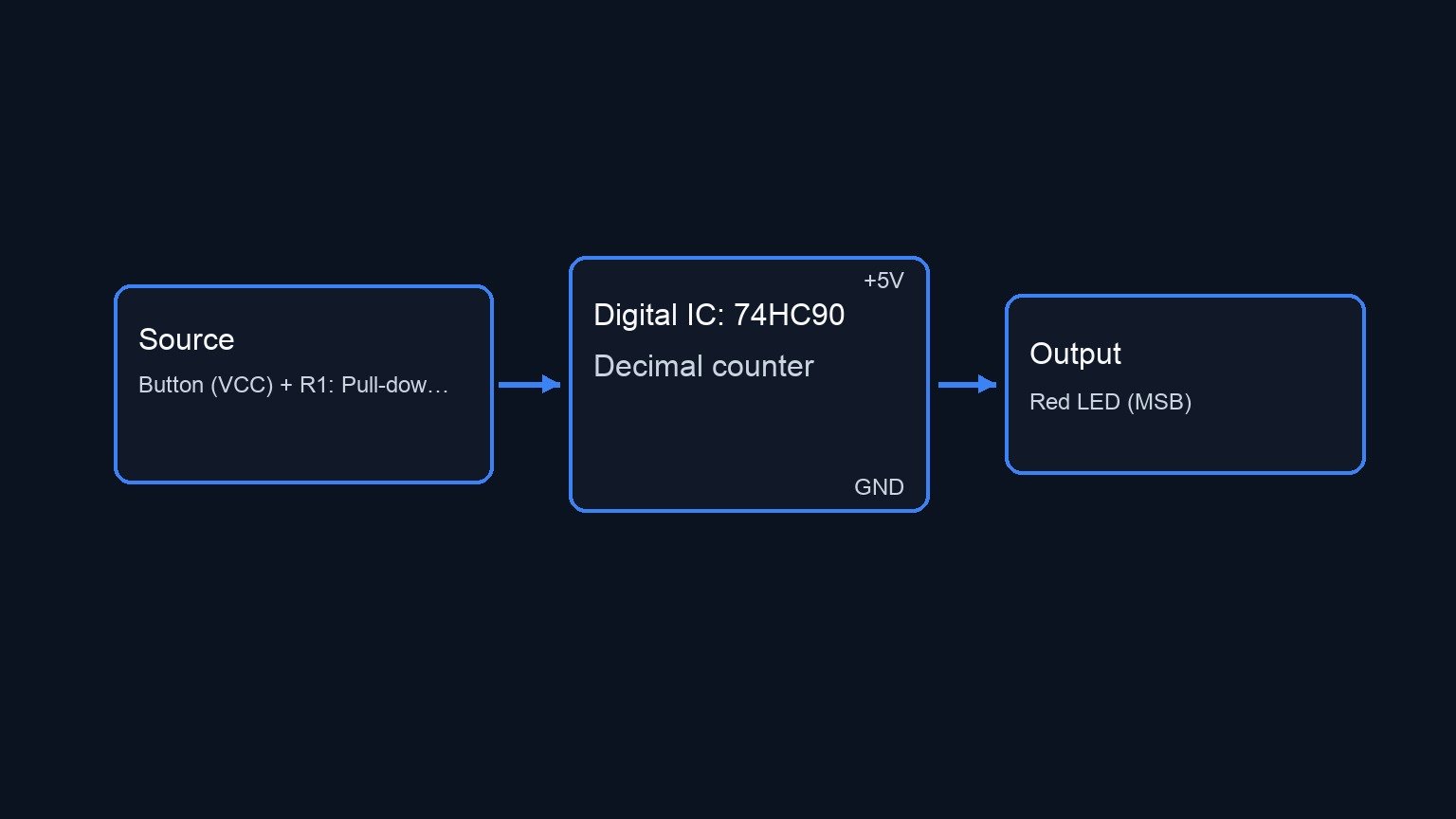
Conceptual block diagram
Schematic
[ VCLK: 1Hz Clock ] ------------------------(CLK)--> [ U1: 74HC90 Decade Counter ] --(QA)--> [ R2: 330 Ω ] --> [ D1: Red LED (LSB) ] --> GND
                                                     [                           ]
[ SW1: Button (VCC) + R1: Pull-down (GND) ] -(RST)-> [ CKA: CLK                  ] --(QB)--> [ R3: 330 Ω ] --> [ D2: Red LED ] --------> GND
                                                     [ MR1, MR2: RST             ]
[ GND ] ------------------------------------(0 V)---> [ MS1, MS2: GND             ] --(QC)--> [ R4: 330 Ω ] --> [ D3: Red LED ] --------> GND
                                                     [ CKB: Connects to QA       ]
                                                     [                           ] --(QD)--> [ R5: 330 Ω ] --> [ D4: Red LED (MSB) ] --> GND
Measurements and tests
- Clock validation: Monitor the CLK node on an oscilloscope or transient plot to verify a consistent square wave.
- Counting sequence: Plot QA, QB, QC, and QD simultaneously. Observe that QA toggles on every falling edge of CLK, and that the binary state progresses correctly from 0000 to 1001.
- BCD Wrap-around: Watch the transition after 1001 (decimal 9). The very next clock pulse should automatically return all outputs (QA–QD) back to 0000 (decimal 0) instead of proceeding to 1010 (decimal 10).
- Manual Reset: While the counter is at any non-zero state (e.g., 0101), actuate SW1. Observe that the RST node spikes to 5 V, forcing QA, QB, QC, and QD to 0000 immediately, ignoring the CLK signal until the button is released.
SPICE netlist and simulation
Reference SPICE Netlist (ngspice) — excerptFull SPICE netlist (ngspice)
* 0 to 9 BCD Decimal Counter
.width out=256

* Power Supply
V1 VCC 0 DC 5

* Clock Source (1 Hz square wave)
VCLK CLK 0 PULSE(0 5 0 0.01 0.01 0.49 1)

* Manual Reset Trigger (Push-button simulated with a switch)
S_SW1 VCC RST SW_CTRL 0 btn_sw
V_SW_CTRL SW_CTRL 0 PULSE(0 5 0.1 0.01 0.01 0.2 20)
.model btn_sw SW(VT=2.5 RON=1 ROFF=100MEG)

* RST Pull-down Resistor
R1 RST 0 10k

* U1: 74HC90 Decade Counter (Behavioral Subcircuit)
X_U1 CLK QA RST RST 0 0 QA QB QC QD VCC 0 IC_7490

* ... (truncated in public view) ...
Copy this content into a .cir file and run with ngspice.
* 0 to 9 BCD Decimal Counter
.width out=256

* Power Supply
V1 VCC 0 DC 5

* Clock Source (1 Hz square wave)
VCLK CLK 0 PULSE(0 5 0 0.01 0.01 0.49 1)

* Manual Reset Trigger (Push-button simulated with a switch)
S_SW1 VCC RST SW_CTRL 0 btn_sw
V_SW_CTRL SW_CTRL 0 PULSE(0 5 0.1 0.01 0.01 0.2 20)
.model btn_sw SW(VT=2.5 RON=1 ROFF=100MEG)

* RST Pull-down Resistor
R1 RST 0 10k

* U1: 74HC90 Decade Counter (Behavioral Subcircuit)
X_U1 CLK QA RST RST 0 0 QA QB QC QD VCC 0 IC_7490

* LEDs and Current Limiting Resistors
R2 QA N_D1 330
D1 N_D1 0 LED_RED

R3 QB N_D2 330
D2 N_D2 0 LED_RED

R4 QC N_D3 330
D3 N_D3 0 LED_RED

R5 QD N_D4 330
D4 N_D4 0 LED_RED

* Red LED Model
.model LED_RED D(IS=1e-19 N=1.6 RS=2.5)

* --- Subcircuits for 7490 Behavioral Model ---
.subckt IC_7490 CKA CKB MR1 MR2 MS1 MS2 QA QB QC QD VCC GND
* Dummy resistors to prevent floating pins if VCC/GND are unused internally
R_VCC VCC 0 100k
R_GND GND 0 1m

* Internal Reset/Set Logic
B_MR MR_int 0 V = (V(MR1)>2.5) * (V(MR2)>2.5) ? 5 : 0
B_MS MS_int 0 V = (V(MS1)>2.5) * (V(MS2)>2.5) ? 5 : 0
B_RST_bc RST_bc 0 V = ((V(MR_int)>2.5) + (V(MS_int)>2.5)) > 0.5 ? 5 : 0

* Divide-by-2 Section (FFa)
B_Da Da 0 V = V(QA)>2.5 ? 0 : 5
X_FFa CKA Da MR_int MS_int QA DFF_FALL

* Divide-by-5 Section (FFb, FFc, FFd)
B_Db Db 0 V = (V(QD)<2.5) * (V(QB)<2.5) ? 5 : 0
X_FFb CKB Db RST_bc 0 QB DFF_FALL

B_Dc Dc 0 V = ( (V(QB)>2.5)*(V(QC)<2.5) + (V(QB)<2.5)*(V(QC)>2.5) ) > 0.5 ? 5 : 0
X_FFc CKB Dc RST_bc 0 QC DFF_FALL

B_Dd Dd 0 V = (V(QB)>2.5) * (V(QC)>2.5) ? 5 : 0
X_FFd CKB Dd MR_int MS_int QD DFF_FALL
.ends

* Falling Edge Triggered D-Flip-Flop
.subckt DFF_FALL CLK D RST SET Q
B_CLK_B CLKB 0 V = V(CLK)>2.5 ? 0 : 5
X_Master CLK D RST SET QM DLATCH
X_Slave CLKB QM RST SET Q DLATCH
.ends

* Analog D-Latch with Reset and Set Priority
.subckt DLATCH EN D RST SET Q
B_Qnext Qnext 0 V = V(RST)>2.5 ? 0 : ( V(SET)>2.5 ? 5 : ( V(EN)>2.5 ? (V(D)>2.5 ? 5 : 0) : V(Q_int) ) )
R1 Qnext Q_int 100
C1 Q_int 0 10n
R2 Q_int 0 1G
E1 Q 0 Q_int 0 1
.ends
* ---------------------------------------------

* Simulation Commands
.op
.tran 0.01 12 0 1m
.print tran V(CLK) V(QA) V(QB) V(QC) V(QD) V(RST)
.end
Simulation Results (Transient Analysis)

Show raw data table (12301 rows)
Index   time            v(clk)          v(qa)           v(qb)           v(qc)           v(qd)           v(rst)
0	0.000000e+00	0.000000e+00	0.000000e+00	0.000000e+00	0.000000e+00	0.000000e+00	4.999500e-04
1	1.000000e-04	5.000000e-02	0.000000e+00	0.000000e+00	0.000000e+00	0.000000e+00	4.999500e-04
2	2.000000e-04	1.000000e-01	0.000000e+00	0.000000e+00	0.000000e+00	0.000000e+00	4.999500e-04
3	4.000000e-04	2.000000e-01	0.000000e+00	0.000000e+00	0.000000e+00	0.000000e+00	4.999500e-04
4	8.000000e-04	4.000000e-01	0.000000e+00	0.000000e+00	0.000000e+00	0.000000e+00	4.999500e-04
5	1.600000e-03	8.000000e-01	0.000000e+00	0.000000e+00	0.000000e+00	0.000000e+00	4.999500e-04
6	2.600000e-03	1.300000e+00	0.000000e+00	0.000000e+00	0.000000e+00	0.000000e+00	4.999500e-04
7	3.600000e-03	1.800000e+00	0.000000e+00	0.000000e+00	0.000000e+00	0.000000e+00	4.999500e-04
8	4.600000e-03	2.300000e+00	0.000000e+00	0.000000e+00	0.000000e+00	0.000000e+00	4.999500e-04
9	5.600000e-03	2.800000e+00	0.000000e+00	0.000000e+00	0.000000e+00	0.000000e+00	4.999500e-04
10	6.310643e-03	3.155321e+00	0.000000e+00	0.000000e+00	0.000000e+00	0.000000e+00	4.999500e-04
11	6.959607e-03	3.479804e+00	0.000000e+00	0.000000e+00	0.000000e+00	0.000000e+00	4.999500e-04
12	7.789270e-03	3.894635e+00	0.000000e+00	0.000000e+00	0.000000e+00	0.000000e+00	4.999500e-04
13	8.789270e-03	4.394635e+00	0.000000e+00	0.000000e+00	0.000000e+00	0.000000e+00	4.999500e-04
14	9.789270e-03	4.894635e+00	0.000000e+00	0.000000e+00	0.000000e+00	0.000000e+00	4.999500e-04
15	1.000000e-02	5.000000e+00	0.000000e+00	0.000000e+00	0.000000e+00	0.000000e+00	4.999500e-04
16	1.010000e-02	5.000000e+00	0.000000e+00	0.000000e+00	0.000000e+00	0.000000e+00	4.999500e-04
17	1.030000e-02	5.000000e+00	0.000000e+00	0.000000e+00	0.000000e+00	0.000000e+00	4.999500e-04
18	1.070000e-02	5.000000e+00	0.000000e+00	0.000000e+00	0.000000e+00	0.000000e+00	4.999500e-04
19	1.150000e-02	5.000000e+00	0.000000e+00	0.000000e+00	0.000000e+00	0.000000e+00	4.999500e-04
20	1.250000e-02	5.000000e+00	0.000000e+00	0.000000e+00	0.000000e+00	0.000000e+00	4.999500e-04
21	1.350000e-02	5.000000e+00	0.000000e+00	0.000000e+00	0.000000e+00	0.000000e+00	4.999500e-04
22	1.450000e-02	5.000000e+00	0.000000e+00	0.000000e+00	0.000000e+00	0.000000e+00	4.999500e-04
23	1.550000e-02	5.000000e+00	0.000000e+00	0.000000e+00	0.000000e+00	0.000000e+00	4.999500e-04
... (12277 more rows) ...
Reference SPICE netlist (ngspice)
* 0 to 9 BCD Decimal Counter
.width out=256

* Power Supply
V1 VCC 0 DC 5

* Clock Source (1 Hz square wave)
VCLK CLK 0 PULSE(0 5 0 0.01 0.01 0.49 1)

* Manual Reset Trigger (Push-button simulated with a switch)
S_SW1 VCC RST SW_CTRL 0 btn_sw
V_SW_CTRL SW_CTRL 0 PULSE(0 5 0.1 0.01 0.01 0.2 20)
.model btn_sw SW(VT=2.5 RON=1 ROFF=100MEG)

* RST Pull-down Resistor
R1 RST 0 10k

* U1: 74HC90 Decade Counter (Behavioral Subcircuit)
X_U1 CLK QA RST RST 0 0 QA QB QC QD VCC 0 IC_7490

* LEDs and Current Limiting Resistors
R2 QA N_D1 330
D1 N_D1 0 LED_RED

R3 QB N_D2 330
D2 N_D2 0 LED_RED

R4 QC N_D3 330
D3 N_D3 0 LED_RED

R5 QD N_D4 330
D4 N_D4 0 LED_RED

* Red LED Model
.model LED_RED D(IS=1e-19 N=1.6 RS=2.5)

* --- Subcircuits for 7490 Behavioral Model ---
.subckt IC_7490 CKA CKB MR1 MR2 MS1 MS2 QA QB QC QD VCC GND
* Dummy resistors to prevent floating pins if VCC/GND are unused internally
R_VCC VCC 0 100k
R_GND GND 0 1m

* Internal Reset/Set Logic
B_MR MR_int 0 V = (V(MR1)>2.5) * (V(MR2)>2.5) ? 5 : 0
B_MS MS_int 0 V = (V(MS1)>2.5) * (V(MS2)>2.5) ? 5 : 0
B_RST_bc RST_bc 0 V = ((V(MR_int)>2.5) + (V(MS_int)>2.5)) > 0.5 ? 5 : 0

* Divide-by-2 Section (FFa)
B_Da Da 0 V = V(QA)>2.5 ? 0 : 5
X_FFa CKA Da MR_int MS_int QA DFF_FALL

* Divide-by-5 Section (FFb, FFc, FFd)
B_Db Db 0 V = (V(QD)2.5)*(V(QC)2.5) ) > 0.5 ? 5 : 0
X_FFc CKB Dc RST_bc 0 QC DFF_FALL

B_Dd Dd 0 V = (V(QB)>2.5) * (V(QC)>2.5) ? 5 : 0
X_FFd CKB Dd MR_int MS_int QD DFF_FALL
.ends

* Falling Edge Triggered D-Flip-Flop
.subckt DFF_FALL CLK D RST SET Q
B_CLK_B CLKB 0 V = V(CLK)>2.5 ? 0 : 5
X_Master CLK D RST SET QM DLATCH
X_Slave CLKB QM RST SET Q DLATCH
.ends

* Analog D-Latch with Reset and Set Priority
.subckt DLATCH EN D RST SET Q
B_Qnext Qnext 0 V = V(RST)>2.5 ? 0 : ( V(SET)>2.5 ? 5 : ( V(EN)>2.5 ? (V(D)>2.5 ? 5 : 0) : V(Q_int) ) )
R1 Qnext Q_int 100
C1 Q_int 0 10n
R2 Q_int 0 1G
E1 Q 0 Q_int 0 1
.ends
* ---------------------------------------------

* Simulation Commands
.op
.tran 0.01 12 0 1m
.print tran V(CLK) V(QA) V(QB) V(QC) V(QD) V(RST)
.end
Simulation Results (Transient Analysis)
Common mistakes and how to avoid them
- Forgetting to connect QA to CKB: The 74HC90 is internally split into a divide-by-2 and a divide-by-5 section. If you do not bridge pin 12 (QA) to pin 1 (CKB), the IC will only count from 0 to 1 and stop, or will not generate the proper BCD sequence.
- Leaving reset pins floating: CMOS logic inputs (like the 74HC series) must never be left disconnected. Leaving MS1, MS2, or the MR pins floating will cause the counter to randomly reset due to ambient electrical noise. Ensure they are tied firmly to 0 or managed via a pull-down resistor.
- Swapping the output bits: Reading the LEDs in the wrong order is very common. Always remember that QA is the Least Significant Bit (LSB, toggles fastest) and QD is the Most Significant Bit (MSB, toggles slowest).
Troubleshooting
- Symptom: All LEDs remain entirely off, and the counter never advances.
- Cause: The Master Reset (MR1 and MR2) or Master Set (MS1 and MS2) pins might be receiving a logic HIGH.
- Fix: Check that SW1 is not stuck closed, ensure R1 (pull-down) is properly connected to ground, and verify MS1/MS2 are wired directly to 0.
- Symptom: The counter counts wildly or skips numbers unexpectedly.
- Cause: The clock signal (CLK) lacks debouncing, or there is missing power supply decoupling.
- Fix: If using a mechanical switch for a clock instead of a clean generator, add a hardware debounce circuit (RC + Schmitt trigger). Additionally, place a 100 nF capacitor directly between VCC and GND near the IC.
- Symptom: The count goes up to 5 and resets (0, 1, 2, 3, 4, 0…).
- Cause: The clock inputs are wired backwards. The clock is entering CKB and cascading into CKA.
- Fix: Ensure the external clock goes exclusively to CKA (pin 14) and QA bridges to CKB (pin 1).
Possible improvements and extensions
- Cascade for 0-99 counting: Add a second 74HC90 IC. Take the QD output of the first stage and feed it into the CKA input of the second stage to create a two-digit decimal counter.
- 7-Segment Display integration: Remove the discrete LEDs and connect QA, QB, QC, and QD into a BCD-to-7-segment decoder IC (like the 74HC47 or CD4511) to display true decimal numerals on a digital display.
More Practical Cases on Prometeo.blog
Find this product and/or books on this topic on Amazon
As an Amazon Associate, I earn from qualifying purchases. If you buy through this link, you help keep this project running.
Quick Quiz

Telecommunications Electronics Engineer and Computer Engineer (official degrees in Spain).