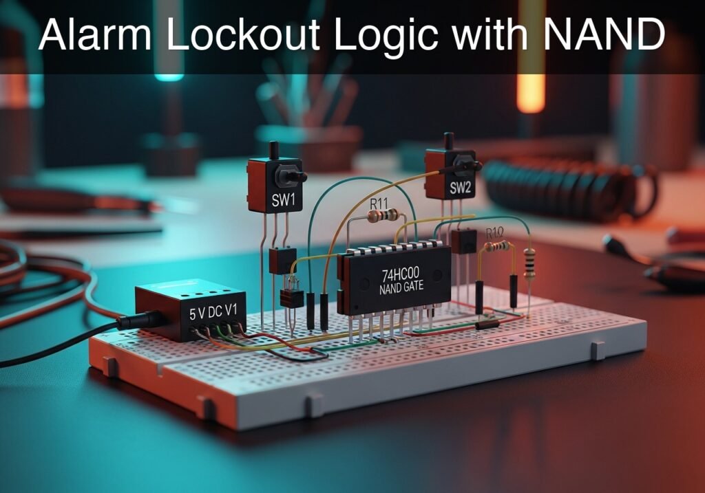
Level: Basic – Build an active-high alarm indicator using 74HC00 NAND gates to understand universal logic and signal inversion.
Objective and use case
You will build a digital logic circuit where an alarm sensor and an enable switch must both be triggered to turn on a warning LED, implemented entirely with a single 74HC00 NAND gate chip.
This circuit is highly useful for demonstrating fundamental digital concepts:
* It demonstrates the concept of «universal gates,» showing how a NAND gate can be wired as a NOT gate (inverter) to achieve an AND logic function.
* It illustrates how an «enable» signal works, which is an industry standard method to authorize or safely block system operations.
* It provides hands-on practice with handling CMOS logic levels and configuring pull-down networks for reliable switch operation.
Expected outcome:
* The intermediate signal (the output of the first NAND gate) will output a logic LOW (0 V) only when both inputs are HIGH (5 V).
* The final output will be logic HIGH (5 V) and will light the LED strictly when both the Alarm and Enable inputs are HIGH.
* You will practically verify the combined truth table of a NAND and a NOT gate.
Target audience: Beginners in digital electronics learning how to manipulate logic gates.
Materials
- V1: 5 V DC supply
- SW1: SPST switch, function: Alarm trigger
- SW2: SPST switch, function: Enable signal
- R1: 10 kΩ resistor, function: pull-down for ALARM node
- R2: 10 kΩ resistor, function: pull-down for ENABLE node
- R3: 330 Ω resistor, function: LED current limiting
- U1: 74HC00 Quad 2-Input NAND Gate, function: logic evaluation and inversion
- D1: Red LED, function: Alarm indicator
Pin-out of the IC used
74HC00 (Quad 2-Input NAND Gate)
| Pin | Name | Logic function | Connection in this case |
|---|---|---|---|
| 1 | 1 A | Input 1 of NAND A | Node ALARM (from SW1) |
| 2 | 1B | Input 2 of NAND A | Node ENABLE (from SW2) |
| 3 | 1Y | Output of NAND A | Node INTERMEDIATE |
| 4 | 2 A | Input 1 of NAND B | Node INTERMEDIATE |
| 5 | 2B | Input 2 of NAND B | Node INTERMEDIATE |
| 6 | 2Y | Output of NAND B | Node VOUT |
| 7 | GND | Ground | Node 0 |
| 14 | VCC | Supply Voltage | Node VCC |
(Note: The 74HC00 contains four independent NAND gates. In this circuit, we use gates A and B. Unused inputs on gates C and D should be tied to ground).
Wiring guide
- V1: connects between VCC and 0.
- SW1: connects between VCC and ALARM.
- R1: connects between ALARM and 0.
- SW2: connects between VCC and ENABLE.
- R2: connects between ENABLE and 0.
- U1 Pin 14 (VCC): connects to VCC.
- U1 Pin 7 (GND): connects to 0.
- U1 Pin 1 (1 A): connects to ALARM.
- U1 Pin 2 (1B): connects to ENABLE.
- U1 Pin 3 (1Y): connects to INTERMEDIATE.
- U1 Pin 4 (2 A): connects to INTERMEDIATE.
- U1 Pin 5 (2B): connects to INTERMEDIATE.
- U1 Pin 6 (2Y): connects to VOUT.
- D1: Anode connects to VOUT, Cathode connects to NODE_LED.
- R3: connects between NODE_LED and 0.
- Safety connection: Connect pins 9, 10, 12, and 13 of U1 to 0 (GND) to prevent unused gates from floating.
Conceptual block diagram
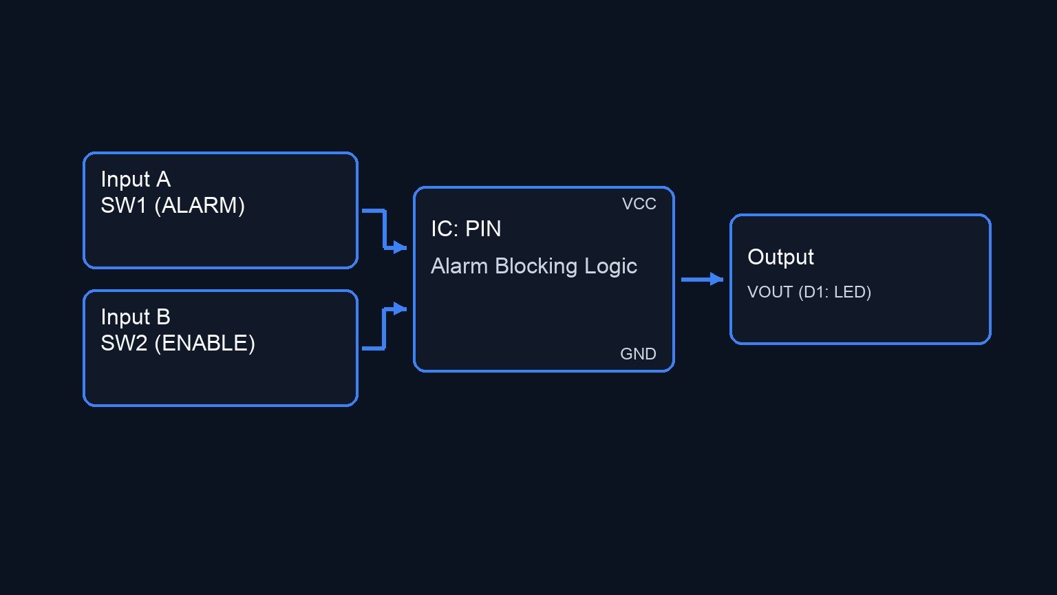
Schematic
VCC --> [ SW1 ] --(ALARM)--> [ U1: Pin 1 (1 A) ]
           |                      |
         [ R1 ]                   |
           |                 [ U1: Gate 1 (NAND) ] --(INTERMEDIATE)--> [ U1: Pins 4,5 (2 A,2B) ]
          GND                     |                                         |
                                  |                                    [ U1: Gate 2 (NAND) ] --(VOUT)--> [ D1: LED ] --(NODE_LED)--> [ R3 ] --> GND
VCC --> [ SW2 ] --(ENABLE)-> [ U1: Pin 2 (1B) ]
           |
         [ R2 ]
           |
          GND

* Power & Safety Connections:
VCC --> [ U1: Pin 14 (VCC) ]
GND <-- [ U1: Pin 7 (GND) ]
GND <-- [ U1: Pins 9, 10, 12, 13 (Unused) ]
Truth table
| Alarm (SW1) | Enable (SW2) | Intermediate Node (1Y) | Output Node (2Y) | LED State |
|---|---|---|---|---|
| 0 | 0 | 1 | 0 | OFF |
| 0 | 1 | 1 | 0 | OFF |
| 1 | 0 | 1 | 0 | OFF |
| 1 | 1 | 0 | 1 | ON |
Measurements and tests
- Use a multimeter to verify the power supply is exactly 5 V across the VCC and 0 nodes.
- Probe the ALARM and ENABLE nodes relative to 0. Verify they read exactly 0 V when their respective switches are open, and 5 V when closed.
- Probe the INTERMEDIATE node. It should read ~5 V when either or both switches are open, and drop to ~0 V strictly when both switches are closed.
- Probe the VOUT node. It should always display the exact opposite logic level of the INTERMEDIATE node.
- Visually confirm that the LED turns on if and only if both switches are toggled to the closed (active) position.
SPICE netlist and simulation
Reference SPICE Netlist (ngspice) — excerptFull SPICE netlist (ngspice)
* Alarm Lockout Logic with NAND

* Main DC Supply
V1 VCC 0 DC 5

* Control signals to simulate user pressing the switches (Testing Truth Table)
V_ctrl1 ctrl1 0 PULSE(0 5 0 1u 1u 50u 100u)
V_ctrl2 ctrl2 0 PULSE(0 5 0 1u 1u 100u 200u)

* SW1: SPST switch (Alarm trigger)
S1 VCC ALARM ctrl1 0 SW_MODEL

* SW2: SPST switch (Enable signal)
S2 VCC ENABLE ctrl2 0 SW_MODEL
.model SW_MODEL SW(VT=2.5 VH=0.5 RON=0.1 ROFF=100MEG)

* Pull-down resistors for logic inputs
R1 ALARM 0 10k
R2 ENABLE 0 10k

* ... (truncated in public view) ...
Copy this content into a .cir file and run with ngspice.
* Alarm Lockout Logic with NAND

* Main DC Supply
V1 VCC 0 DC 5

* Control signals to simulate user pressing the switches (Testing Truth Table)
V_ctrl1 ctrl1 0 PULSE(0 5 0 1u 1u 50u 100u)
V_ctrl2 ctrl2 0 PULSE(0 5 0 1u 1u 100u 200u)

* SW1: SPST switch (Alarm trigger)
S1 VCC ALARM ctrl1 0 SW_MODEL

* SW2: SPST switch (Enable signal)
S2 VCC ENABLE ctrl2 0 SW_MODEL
.model SW_MODEL SW(VT=2.5 VH=0.5 RON=0.1 ROFF=100MEG)

* Pull-down resistors for logic inputs
R1 ALARM 0 10k
R2 ENABLE 0 10k

* U1: 74HC00 Quad 2-Input NAND Gate
* Pinout: 1:1A, 2:1B, 3:1Y, 4:2A, 5:2B, 6:2Y, 7:GND, 8:3Y, 9:3A, 10:3B, 11:4Y, 12:4A, 13:4B, 14:VCC
XU1 ALARM ENABLE INTERMEDIATE INTERMEDIATE INTERMEDIATE VOUT 0 NC8 0 0 NC11 0 0 VCC HC00_DIP14

* D1: Red LED (Alarm indicator)
D1 VOUT NODE_LED DLED
.model DLED D(IS=1e-20 N=2.2 RS=15)

* R3: LED current limiting resistor
R3 NODE_LED 0 330

* Subcircuit for 74HC00 (Quad 2-Input NAND Gate)
.subckt HC00_DIP14 1 2 3 4 5 6 7 8 9 10 11 12 13 14
* Gate 1
B1 3_int 7 V=V(14)*(1-(1/(1+exp(-50*(V(1)-2.5))))*(1/(1+exp(-50*(V(2)-2.5)))))
R1 3_int 3 50
* Gate 2
B2 6_int 7 V=V(14)*(1-(1/(1+exp(-50*(V(4)-2.5))))*(1/(1+exp(-50*(V(5)-2.5)))))
R2 6_int 6 50
* Gate 3
B3 8_int 7 V=V(14)*(1-(1/(1+exp(-50*(V(9)-2.5))))*(1/(1+exp(-50*(V(10)-2.5)))))
R3 8_int 8 50
* Gate 4
B4 11_int 7 V=V(14)*(1-(1/(1+exp(-50*(V(12)-2.5))))*(1/(1+exp(-50*(V(13)-2.5)))))
R4 11_int 11 50
.ends

* Analysis directives
.tran 1u 500u
.print tran V(ALARM) V(ENABLE) V(VOUT) V(NODE_LED)
.op
.end
Simulation Results (Transient Analysis)

Show raw data table (691 rows)
Index   time            v(alarm)        v(enable)       v(vout)         v(node_led)
0	0.000000e+00	4.999500e-04	4.999500e-04	1.047185e-47	-6.91142e-47
1	1.000000e-08	4.999500e-04	4.999500e-04	7.268458e-64	-4.79767e-63
2	2.000000e-08	4.999500e-04	4.999500e-04	-7.26994e-64	4.797672e-63
3	4.000000e-08	4.999500e-04	4.999500e-04	-7.41841e-68	-2.28156e-77
4	8.000000e-08	4.999500e-04	4.999500e-04	-7.41841e-68	-2.51468e-77
5	1.600000e-07	4.999500e-04	4.999500e-04	-7.41841e-68	-2.44808e-77
6	3.200000e-07	4.999500e-04	4.999500e-04	-7.41841e-68	-2.44808e-77
7	3.750000e-07	4.999500e-04	4.999500e-04	-7.41841e-68	-2.44808e-77
8	4.712500e-07	4.999500e-04	4.999500e-04	-7.41841e-68	-2.44808e-77
9	4.978906e-07	4.999500e-04	4.999500e-04	-7.41841e-68	-2.44808e-77
10	5.445117e-07	4.999500e-04	4.999500e-04	-7.41841e-68	-2.44808e-77
11	5.574158e-07	4.999500e-04	4.999500e-04	-7.41841e-68	-2.44808e-77
12	5.799979e-07	4.999500e-04	4.999500e-04	-7.41841e-68	-2.44808e-77
13	6.049995e-07	4.999950e+00	4.999950e+00	4.662865e+00	2.225088e+00
14	6.550027e-07	4.999950e+00	4.999950e+00	4.662939e+00	2.224602e+00
15	7.550091e-07	4.999950e+00	4.999950e+00	4.662792e+00	2.225571e+00
16	9.550219e-07	4.999950e+00	4.999950e+00	4.662792e+00	2.225574e+00
17	1.000000e-06	4.999950e+00	4.999950e+00	4.662786e+00	2.225611e+00
18	1.040003e-06	4.999950e+00	4.999950e+00	4.662786e+00	2.225611e+00
19	1.120008e-06	4.999950e+00	4.999950e+00	4.662786e+00	2.225611e+00
20	1.280018e-06	4.999950e+00	4.999950e+00	4.662786e+00	2.225611e+00
21	1.600038e-06	4.999950e+00	4.999950e+00	4.662786e+00	2.225611e+00
22	2.240079e-06	4.999950e+00	4.999950e+00	4.662786e+00	2.225611e+00
23	3.240079e-06	4.999950e+00	4.999950e+00	4.662786e+00	2.225611e+00
... (667 more rows) ...
Reference SPICE netlist (ngspice)
* Alarm Lockout Logic with NAND

* Main DC Supply
V1 VCC 0 DC 5

* Control signals to simulate user pressing the switches (Testing Truth Table)
V_ctrl1 ctrl1 0 PULSE(0 5 0 1u 1u 50u 100u)
V_ctrl2 ctrl2 0 PULSE(0 5 0 1u 1u 100u 200u)

* SW1: SPST switch (Alarm trigger)
S1 VCC ALARM ctrl1 0 SW_MODEL

* SW2: SPST switch (Enable signal)
S2 VCC ENABLE ctrl2 0 SW_MODEL
.model SW_MODEL SW(VT=2.5 VH=0.5 RON=0.1 ROFF=100MEG)

* Pull-down resistors for logic inputs
R1 ALARM 0 10k
R2 ENABLE 0 10k

* U1: 74HC00 Quad 2-Input NAND Gate
* Pinout: 1:1A, 2:1B, 3:1Y, 4:2A, 5:2B, 6:2Y, 7:GND, 8:3Y, 9:3A, 10:3B, 11:4Y, 12:4A, 13:4B, 14:VCC
XU1 ALARM ENABLE INTERMEDIATE INTERMEDIATE INTERMEDIATE VOUT 0 NC8 0 0 NC11 0 0 VCC HC00_DIP14

* D1: Red LED (Alarm indicator)
D1 VOUT NODE_LED DLED
.model DLED D(IS=1e-20 N=2.2 RS=15)

* R3: LED current limiting resistor
R3 NODE_LED 0 330

* Subcircuit for 74HC00 (Quad 2-Input NAND Gate)
.subckt HC00_DIP14 1 2 3 4 5 6 7 8 9 10 11 12 13 14
* Gate 1
B1 3_int 7 V=V(14)*(1-(1/(1+exp(-50*(V(1)-2.5))))*(1/(1+exp(-50*(V(2)-2.5)))))
R1 3_int 3 50
* Gate 2
B2 6_int 7 V=V(14)*(1-(1/(1+exp(-50*(V(4)-2.5))))*(1/(1+exp(-50*(V(5)-2.5)))))
R2 6_int 6 50
* Gate 3
B3 8_int 7 V=V(14)*(1-(1/(1+exp(-50*(V(9)-2.5))))*(1/(1+exp(-50*(V(10)-2.5)))))
R3 8_int 8 50
* Gate 4
B4 11_int 7 V=V(14)*(1-(1/(1+exp(-50*(V(12)-2.5))))*(1/(1+exp(-50*(V(13)-2.5)))))
R4 11_int 11 50
.ends

* Analysis directives
.tran 1u 500u
.print tran V(ALARM) V(ENABLE) V(VOUT) V(NODE_LED)
.op
.end
Simulation Results (Transient Analysis)
Common mistakes and how to avoid them
- Leaving unused inputs floating: CMOS chips like the 74HC00 are highly sensitive to static and ambient noise. Unused gate inputs (pins 9, 10, 12, 13) must be explicitly tied to ground (0) or VCC.
- Omitting the pull-down resistors: Without R1 and R2, the input pins will float when the switches are open, leading to unpredictable, flickering behavior in the LED. Always ensure the 10 kΩ pull-downs are securely connected to ground.
- Connecting the LED without a series resistor: Connecting D1 directly between VOUT and 0 will draw excessive current, potentially destroying the LED and burning out the output stage of the 74HC00 chip. R3 is mandatory.
Troubleshooting
- Symptom: The LED never turns off, regardless of switch positions.
- Cause: One of the input pull-down resistors is loose, causing the chip to read a false HIGH, or the intermediate node isn’t wired correctly to both inputs of the second gate.
- Fix: Verify connections for R1 and R2 to ground. Ensure U1 Pin 3 routes precisely to both Pin 4 and Pin 5.
- Symptom: The LED brightness flickers when a hand is moved near the circuit.
- Cause: A floating input is acting as an antenna and picking up environmental noise.
- Fix: Check that all unused inputs on the IC are tied to ground, and ensure R1 and R2 are seated firmly in the breadboard.
- Symptom: The IC becomes hot to the touch.
- Cause: The power supply is connected backwards, or the output node is shorted directly to ground or VCC.
- Fix: Disconnect power immediately. Verify that U1 Pin 14 goes strictly to +5 V and Pin 7 goes strictly to Ground.
Possible improvements and extensions
- Master Override switch: Introduce a third switch and utilize one of the spare NAND gates (e.g., Gate C) to create a «Master Override» that forces the LED off regardless of the Alarm and Enable signals.
- Add a delay circuit: Incorporate an RC network (a resistor and a capacitor) between one of the switches and its input pin. This requires the switch to be held closed for a specific duration before the logic gate registers a HIGH signal, preventing false alarms.
More Practical Cases on Prometeo.blog
Find this product and/or books on this topic on Amazon
As an Amazon Associate, I earn from qualifying purchases. If you buy through this link, you help keep this project running.
Quick Quiz

Telecommunications Electronics Engineer and Computer Engineer (official degrees in Spain).