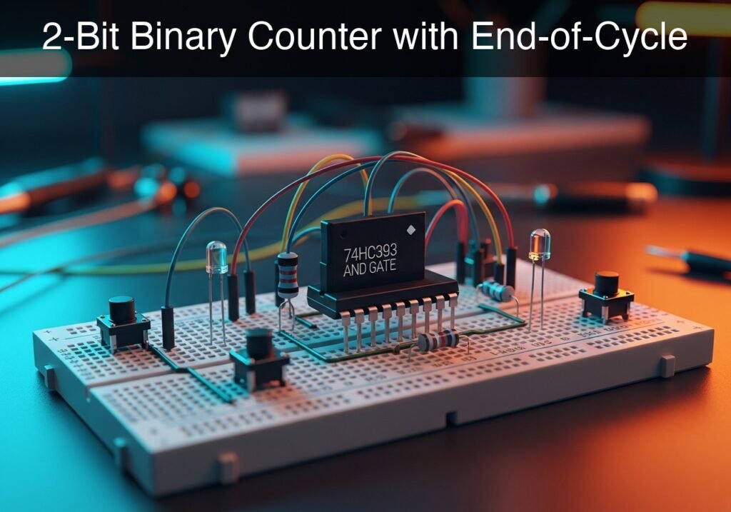
Level: Basic – Build a 0 to 3 binary counter with manual clock, reset, and a maximum count indicator.
Objective and use case
In this practical case, you will build a 2-bit digital counter using a 74HC393 IC and decode its maximum state (binary 11, decimal 3) using a 74HC08 AND gate. A simulated clock pushbutton increments the count, while a manual reset pushbutton forces the counter back to zero.
Why this is useful:
* Demonstrates how sequential logic (counters) tracks discrete events over time.
* Shows how combinational logic (AND gate) is used to decode specific binary states and trigger events.
* Provides a foundational understanding of clock edge triggering and asynchronous resets.
* Acts as a building block for state machines, timers, and step-sequencers in industrial or hobbyist electronics.
Expected outcome:
* Pressing and releasing the clock button will advance the binary state sequentially: 00 → 01 → 10 → 11.
* Two LEDs will display the current binary count (LSB and MSB).
* A third LED (end-of-cycle indicator) will light up strictly when the count reaches state 3.
* Pressing the reset button will immediately extinguish all LEDs, returning the circuit to state 00 regardless of the current count.
* Target audience: Electronics beginners learning digital logic and basic state tracking.
Materials
- V1: 5 V DC supply
- S1: normally open pushbutton, function: clock pulse generator
- S2: normally open pushbutton, function: manual reset trigger
- R1: 10 kΩ resistor, function: pull-down for CLK node
- R2: 10 kΩ resistor, function: pull-down for MR node
- R3: 330 Ω resistor, function: current limiting for QA LED
- R4: 330 Ω resistor, function: current limiting for QB LED
- R5: 330 Ω resistor, function: current limiting for MAX_VAL LED
- D1: green LED, function: LSB indicator (QA)
- D2: yellow LED, function: MSB indicator (QB)
- D3: red LED, function: end-of-cycle indicator
- U1: 74HC393 dual 4-bit binary counter, function: state counting
- U2: 74HC08 quad 2-input AND gate, function: state decoding
Pin-out of the IC used
74HC393 (Dual 4-Bit Binary Counter – Only Half Used)
| Pin | Name | Logic function | Connection in this case |
|---|---|---|---|
| 1 | 1CP | Clock Input (Active Low / Falling Edge) | CLK |
| 2 | 1MR | Master Reset (Active High) | MR |
| 3 | 1Q0 | Output 0 (LSB) | QA |
| 4 | 1Q1 | Output 1 (MSB) | QB |
| 7 | GND | Ground | 0 |
| 14 | VCC | Positive Supply | VCC |
Note: Pins 5, 6, and 8 through 13 belong to the second counter and can be grounded in a real circuit to prevent floating inputs.
74HC08 (Quad 2-Input AND Gate – Only One Gate Used)
| Pin | Name | Logic function | Connection in this case |
|---|---|---|---|
| 1 | 1 A | Input A of Gate 1 | QA |
| 2 | 1B | Input B of Gate 1 | QB |
| 3 | 1Y | Output of Gate 1 | MAX_VAL |
| 7 | GND | Ground | 0 |
| 14 | VCC | Positive Supply | VCC |
Wiring guide
- V1: connects between VCC and 0.
- S1: connects between VCC and CLK.
- R1: connects between CLK and 0.
- S2: connects between VCC and MR.
- R2: connects between MR and 0.
- U1: Pin 1 connects to CLK, Pin 2 connects to MR, Pin 3 connects to QA, Pin 4 connects to QB, Pin 7 connects to 0, Pin 14 connects to VCC.
- U2: Pin 1 connects to QA, Pin 2 connects to QB, Pin 3 connects to MAX_VAL, Pin 7 connects to 0, Pin 14 connects to VCC.
- R3: connects between QA and N_D1.
- D1: connects between N_D1 and 0 (anode to N_D1, cathode to 0).
- R4: connects between QB and N_D2.
- D2: connects between N_D2 and 0 (anode to N_D2, cathode to 0).
- R5: connects between MAX_VAL and N_D3.
- D3: connects between N_D3 and 0 (anode to N_D3, cathode to 0).
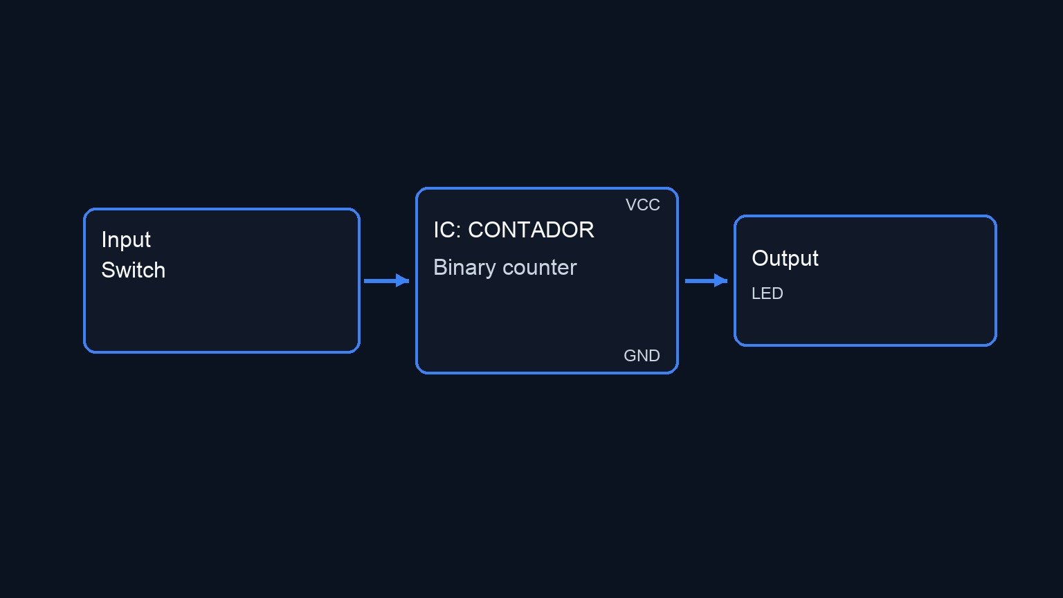
Conceptual block diagram
Schematic
[ S1 (Clock) + R1 ] --(CLK)--> [                       ] --(QA)--> [ R3 (330 Ω) ] --> [ D1 (Green LED) ] ---> GND
                               [                       ]
                               [                       ] --(QA)--> [                       ]
                               [ U1: 74HC393 Counter   ]           [ U2: 74HC08 AND Gate   ] --(MAX_VAL)--> [ R5 (330 Ω) ] --> [ D3 (Red LED) ] ---> GND
                               [                       ] --(QB)--> [                       ]
                               [                       ]
[ S2 (Reset) + R2 ] --(MR)---> [                       ] --(QB)--> [ R4 (330 Ω) ] --> [ D2 (Yellow LED) ] --> GND
Measurements and tests
- Initial State Check: Power on the circuit. If any LEDs are lit, press and release S2 (Master Reset). The voltage at the MR node will spike to 5 V, clearing the counter. Measure QA, QB, and MAX_VAL; all should be 0 V. All LEDs must be OFF.
- First Clock Pulse (State 1): Press and hold S1. The CLK node goes to 5 V. Release S1. The 74HC393 triggers on the falling edge (high-to-low transition). D1 (QA) should turn on. D2 (QB) and D3 (MAX_VAL) remain off.
- Second Clock Pulse (State 2): Press and release S1 again. D1 turns off and D2 turns on. This represents binary 10 (decimal 2).
- Third Clock Pulse (State 3): Press and release S1 a third time. Both D1 (QA) and D2 (QB) turn on. Consequently, inputs 1 A and 1B on the 74HC08 are both HIGH. The MAX_VAL node will output 5 V, lighting up the end-of-cycle LED (D3).
- Rollover (State 0): Press and release S1 a fourth time. The counter overflows the 2-bit capacity represented by QA and QB. Both counting LEDs and the MAX_VAL LED will turn off.
- Asynchronous Reset Verification: Cycle the counter to state 2 or 3. Press the reset button S2. Observe that the counter immediately resets to 00 without waiting for a clock pulse.
SPICE netlist and simulation
Reference SPICE Netlist (ngspice) — excerptFull SPICE netlist (ngspice)
* Practical case: 2-Bit Binary Counter with End-of-Cycle

.width out=256

* --- Power Supply ---
V1 VCC 0 DC 5

* --- User Inputs (Pushbuttons modeled as Voltage-Controlled Switches) ---
* Clock Pushbutton (S1) connects VCC to CLK
S1 VCC CLK S1_ctrl 0 mySW
Vctrl1 S1_ctrl 0 PULSE(0 5 20u 1u 1u 40u 100u)
R1 CLK 0 10k

* Manual Reset Pushbutton (S2) connects VCC to MR
S2 VCC MR S2_ctrl 0 mySW
* Initialize reset at start, then trigger again at 280us to clear the MAX_VAL state
Vctrl2 S2_ctrl 0 PWL(0 5 10u 5 11u 0 280u 0 281u 5 290u 5 291u 0)
R2 MR 0 10k

.model mySW SW(Ron=1 Roff=100Meg Vt=2.5 Vh=0.5)
* ... (truncated in public view) ...
Copy this content into a .cir file and run with ngspice.
* Practical case: 2-Bit Binary Counter with End-of-Cycle

.width out=256

* --- Power Supply ---
V1 VCC 0 DC 5

* --- User Inputs (Pushbuttons modeled as Voltage-Controlled Switches) ---
* Clock Pushbutton (S1) connects VCC to CLK
S1 VCC CLK S1_ctrl 0 mySW
Vctrl1 S1_ctrl 0 PULSE(0 5 20u 1u 1u 40u 100u)
R1 CLK 0 10k

* Manual Reset Pushbutton (S2) connects VCC to MR
S2 VCC MR S2_ctrl 0 mySW
* Initialize reset at start, then trigger again at 280us to clear the MAX_VAL state
Vctrl2 S2_ctrl 0 PWL(0 5 10u 5 11u 0 280u 0 281u 5 290u 5 291u 0)
R2 MR 0 10k

.model mySW SW(Ron=1 Roff=100Meg Vt=2.5 Vh=0.5)
.model logic_sw SW(Ron=1k Roff=100Meg Vt=2.5 Vh=0.1)

* --- Subcircuits for Logic ---

* Falling-edge triggered T-Flip-Flop with active-high asynchronous reset
.subckt TFF_falling CLK CLR Q
B1 CLK_b 0 V=5-V(CLK)
S1 Q_b master CLK 0 logic_sw
C1 master 0 100p
R1 master 0 1G
S2 master slave CLK_b 0 logic_sw
C2 slave 0 100p
R2 slave 0 1G
* Asynchronous Reset Switches
S3 master 0 CLR 0 logic_sw
S4 slave 0 CLR 0 logic_sw
* Output formatting with RC filter to prevent timestep discontinuities
B2 Q_raw 0 V=V(slave)>2.5?5:0
R3 Q_raw Q 1k
C3 Q 0 100p
B4 Q_b 0 V=5-V(Q_raw)
.ends

* U1: 74HC393 Dual 4-bit Binary Counter (Only first 2 bits QA, QB modeled)
.subckt 74HC393 CLK MR QA QB GND VCC
X1 CLK MR QA TFF_falling
X2 QA MR QB TFF_falling
.ends

* U2: 74HC08 Quad 2-input AND Gate
.subckt 74HC08 A B Y GND VCC
B1 Y_raw 0 V=(V(A)>2.5)&&(V(B)>2.5)?5:0
R1 Y_raw Y 1k
C1 Y 0 100p
.ends

* --- Main Circuit ---

* U1: 74HC393 Dual 4-bit Binary Counter
XU1 CLK MR QA QB 0 VCC 74HC393

* U2: 74HC08 Quad 2-input AND gate
XU2 QA QB MAX_VAL 0 VCC 74HC08

* --- Output LEDs ---
R3 QA N_D1 330
D1 N_D1 0 LED_green

R4 QB N_D2 330
D2 N_D2 0 LED_yellow

R5 MAX_VAL N_D3 330
D3 N_D3 0 LED_red

.model LED_green D(IS=1e-19 N=1.8 RS=10)
.model LED_yellow D(IS=1e-19 N=1.7 RS=10)
.model LED_red D(IS=1e-19 N=1.6 RS=10)

* --- Simulation and Output ---
.op
.tran 1u 600u
.print tran V(CLK) V(MR) V(QA) V(QB) V(MAX_VAL)
.end
Simulation Results (Transient Analysis)

Show raw data table (1035 rows)
Index   time            v(clk)          v(mr)           v(qa)           v(qb)           v(max_val)
0	0.000000e+00	4.999500e-04	4.999500e+00	1.094960e-64	1.402927e-64	1.824146e-64
1	1.000000e-08	4.999500e-04	4.999500e+00	9.954179e-65	1.275388e-64	1.658315e-64
2	2.000000e-08	4.999500e-04	4.999500e+00	9.049254e-65	1.159444e-64	1.507559e-64
3	4.000000e-08	4.999500e-04	4.999500e+00	7.403935e-65	9.486357e-65	1.233457e-64
4	8.000000e-08	4.999500e-04	4.999500e+00	4.935957e-65	6.324238e-65	8.223048e-65
5	1.600000e-07	4.999500e-04	4.999500e+00	2.115410e-65	2.710388e-65	3.524164e-65
6	3.200000e-07	4.999500e-04	4.999500e+00	2.350456e-66	3.011542e-66	3.915737e-66
7	6.400000e-07	4.999500e-04	4.999500e+00	-5.42413e-67	-6.94971e-67	-9.03632e-67
8	1.280000e-06	4.999500e-04	4.999500e+00	2.841210e-67	3.640325e-67	4.733309e-67
9	2.280000e-06	4.999500e-04	4.999500e+00	-1.89414e-67	-2.42688e-67	-3.15554e-67
10	3.280000e-06	4.999500e-04	4.999500e+00	1.262760e-67	1.617922e-67	2.103693e-67
11	4.280000e-06	4.999500e-04	4.999500e+00	-8.41840e-68	-1.07861e-67	-1.40246e-67
12	5.280000e-06	4.999500e-04	4.999500e+00	5.612267e-68	7.190766e-68	9.349746e-68
13	6.280000e-06	4.999500e-04	4.999500e+00	-3.74151e-68	-4.79384e-68	-6.23316e-68
14	7.280000e-06	4.999500e-04	4.999500e+00	2.494341e-68	3.195896e-68	4.155443e-68
15	8.280000e-06	4.999500e-04	4.999500e+00	-1.66289e-68	-2.13060e-68	-2.77030e-68
16	9.280000e-06	4.999500e-04	4.999500e+00	1.108596e-68	1.420398e-68	1.846863e-68
17	1.000000e-05	4.999500e-04	4.999500e+00	-6.26598e-69	-8.02834e-69	-1.04388e-68
18	1.010000e-05	4.999500e-04	4.999500e+00	-3.13299e-69	-4.01417e-69	-5.21940e-69
19	1.030000e-05	4.999500e-04	4.999500e+00	1.566513e-78	2.007109e-78	2.609729e-78
20	1.035875e-05	4.999500e-04	4.999500e+00	8.551514e-79	1.095671e-78	1.424639e-78
21	1.046156e-05	4.999500e-04	4.999500e+00	2.744610e-79	3.516558e-79	4.572383e-79
22	1.049002e-05	4.999500e-04	4.999500e+00	2.060863e-79	2.640500e-79	3.433294e-79
23	1.053982e-05	4.999500e-04	4.999500e+00	1.239160e-79	1.587686e-79	2.064379e-79
... (1011 more rows) ...
Reference SPICE netlist (ngspice)
* Practical case: 2-Bit Binary Counter with End-of-Cycle

.width out=256

* --- Power Supply ---
V1 VCC 0 DC 5

* --- User Inputs (Pushbuttons modeled as Voltage-Controlled Switches) ---
* Clock Pushbutton (S1) connects VCC to CLK
S1 VCC CLK S1_ctrl 0 mySW
Vctrl1 S1_ctrl 0 PULSE(0 5 20u 1u 1u 40u 100u)
R1 CLK 0 10k

* Manual Reset Pushbutton (S2) connects VCC to MR
S2 VCC MR S2_ctrl 0 mySW
* Initialize reset at start, then trigger again at 280us to clear the MAX_VAL state
Vctrl2 S2_ctrl 0 PWL(0 5 10u 5 11u 0 280u 0 281u 5 290u 5 291u 0)
R2 MR 0 10k

.model mySW SW(Ron=1 Roff=100Meg Vt=2.5 Vh=0.5)
.model logic_sw SW(Ron=1k Roff=100Meg Vt=2.5 Vh=0.1)

* --- Subcircuits for Logic ---

* Falling-edge triggered T-Flip-Flop with active-high asynchronous reset
.subckt TFF_falling CLK CLR Q
B1 CLK_b 0 V=5-V(CLK)
S1 Q_b master CLK 0 logic_sw
C1 master 0 100p
R1 master 0 1G
S2 master slave CLK_b 0 logic_sw
C2 slave 0 100p
R2 slave 0 1G
* Asynchronous Reset Switches
S3 master 0 CLR 0 logic_sw
S4 slave 0 CLR 0 logic_sw
* Output formatting with RC filter to prevent timestep discontinuities
B2 Q_raw 0 V=V(slave)>2.5?5:0
R3 Q_raw Q 1k
C3 Q 0 100p
B4 Q_b 0 V=5-V(Q_raw)
.ends

* U1: 74HC393 Dual 4-bit Binary Counter (Only first 2 bits QA, QB modeled)
.subckt 74HC393 CLK MR QA QB GND VCC
X1 CLK MR QA TFF_falling
X2 QA MR QB TFF_falling
.ends

* U2: 74HC08 Quad 2-input AND Gate
.subckt 74HC08 A B Y GND VCC
B1 Y_raw 0 V=(V(A)>2.5)&&(V(B)>2.5)?5:0
R1 Y_raw Y 1k
C1 Y 0 100p
.ends

* --- Main Circuit ---

* U1: 74HC393 Dual 4-bit Binary Counter
XU1 CLK MR QA QB 0 VCC 74HC393

* U2: 74HC08 Quad 2-input AND gate
XU2 QA QB MAX_VAL 0 VCC 74HC08

* --- Output LEDs ---
R3 QA N_D1 330
D1 N_D1 0 LED_green

R4 QB N_D2 330
D2 N_D2 0 LED_yellow

R5 MAX_VAL N_D3 330
D3 N_D3 0 LED_red

.model LED_green D(IS=1e-19 N=1.8 RS=10)
.model LED_yellow D(IS=1e-19 N=1.7 RS=10)
.model LED_red D(IS=1e-19 N=1.6 RS=10)

* --- Simulation and Output ---
.op
.tran 1u 600u
.print tran V(CLK) V(MR) V(QA) V(QB) V(MAX_VAL)
.end
Simulation Results (Transient Analysis)
Common mistakes and how to avoid them
- Ignoring switch bounce: Mechanical pushbuttons exhibit «bounce,» creating multiple rapid voltage transitions on a single press. This causes the counter to skip numbers. Avoid this in critical applications by using a hardware debounce circuit (like an RC filter followed by a Schmitt trigger).
- Misunderstanding the clock edge: The 74HC393 increments on the falling edge of the clock signal. Beginners often expect the count to increase the moment the button is pressed, but it actually increases the moment the button is released (when the voltage drops from 5 V to 0 V).
- Leaving unused logic inputs floating: While this basic test circuit focuses on the used gates, leaving the inputs of the unused gates on the 74HC393 and 74HC08 floating can cause internal oscillation and excessive power draw. Always tie unused inputs to GND or VCC.
Troubleshooting
- Symptom: The counter jumps randomly (e.g., skips from 0 to 2 or 3).
- Cause: Mechanical switch bounce on S1 is sending multiple clock pulses instantly.
- Fix: Add a 100 nF capacitor in parallel with R1 to filter out the rapid mechanical bounces, or press the button very deliberately.
- Symptom: The counter never increments; LEDs remain off.
- Cause: The master reset pin is stuck HIGH, keeping the counter constantly cleared.
- Fix: Check R2. Ensure it is firmly connected to GND to pull the MR node LOW when the reset button is not pressed.
- Symptom: LEDs D1 and D2 count correctly, but D3 never turns on.
- Cause: The 74HC08 AND gate is not receiving power, or its inputs are incorrectly wired.
- Fix: Verify that pins 14 (VCC) and 7 (GND) of U2 are connected. Double-check that pin 1 connects to QA and pin 2 connects to QB.
- Symptom: LEDs are very dim or burn out instantly.
- Cause: Incorrect or missing current-limiting resistors.
- Fix: Ensure R3, R4, and R5 (330 Ω) are properly placed in series with the respective LED anodes.
Possible improvements and extensions
- Hardware Debouncing with a Schmitt Trigger: Replace the simple S1/R1 clock with an RC network fed into a 74HC14 Schmitt trigger inverter to completely eliminate switch bounce and provide perfectly clean clock edges.
- Auto-Reset for Modulo-3 Counting: Connect the MAX_VAL output (pin 3 of U2) directly to the Master Reset input (MR, pin 2 of U1) instead of using the manual S2 switch. This will automatically clear the counter the instant it hits state 3, turning it into a 0-to-2 recurring cycle counter.
More Practical Cases on Prometeo.blog
Find this product and/or books on this topic on Amazon
As an Amazon Associate, I earn from qualifying purchases. If you buy through this link, you help keep this project running.
Quick Quiz

Telecommunications Electronics Engineer and Computer Engineer (official degrees in Spain).