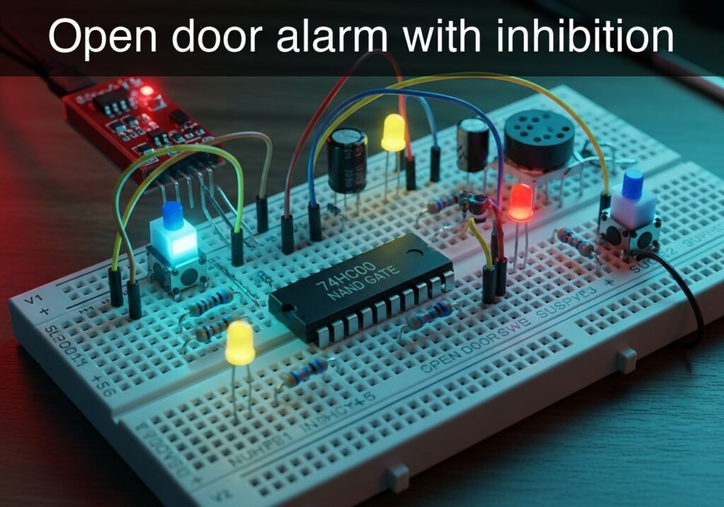
Level: Basic – Design a logic circuit using a 74HC00 NAND gate to trigger an LED alarm only when the door is open and the system is enabled.
Objective and use case
What you will build is a basic security system logic controller using the universal 74HC00 NAND chip. The circuit processes two discrete inputs (a door sensor and an enable switch) to activate a visual alarm strictly when the system is armed and a breach occurs.
Why it is useful:
* It demonstrates how multiple NAND gates can be combined to form an AND logic gate.
* It illustrates the concept of a hardware «enable/inhibit» signal commonly used in industrial and digital electronics.
* It provides practical experience in interfacing mechanical switches with digital CMOS inputs without floating states.
Expected outcome:
* When the door switch is open (Logic 1) AND the enable switch is closed (Logic 1), the LED turns ON.
* If the enable switch is open (Logic 0), the alarm remains inhibited (LED OFF) regardless of the door state.
* Logic High (VCC) and Logic Low (0 V) voltages can be clearly measured at the switch output nodes.
* The intermediate logic signal between the two NAND gates will correctly show the inverted state of the final output.
Target audience and level: Electronics beginners learning digital logic and combinational circuits.
Materials
- V1: 5 V DC supply, function: main circuit power
- SW1: SPST switch, function: door sensor (closed = logic 0, open = logic 1)
- SW2: SPST switch, function: system enable (inhibited = logic 0, armed = logic 1)
- R1: 10 kΩ resistor, function: pull-down for SW1 at node DOOR
- R2: 10 kΩ resistor, function: pull-down for SW2 at node EN
- R3: 330 Ω resistor, function: LED current limiting
- U1: 74HC00 quad 2-input NAND gate, function: logic processing
- D1: red LED, function: visual alarm indicator
Pin-out of the IC used
IC used: 74HC00 (Quad 2-Input NAND Gate)
| Pin | Name | Logic function | Connection in this case |
|---|---|---|---|
| 1 | 1 A | Input A of Gate 1 | Node DOOR (from SW1) |
| 2 | 1B | Input B of Gate 1 | Node EN (from SW2) |
| 3 | 1Y | Output of Gate 1 | Node NAND_OUT |
| 4 | 2 A | Input A of Gate 2 | Node NAND_OUT (tied to 2B) |
| 5 | 2B | Input B of Gate 2 | Node NAND_OUT (tied to 2 A) |
| 6 | 2Y | Output of Gate 2 | Node ALARM |
| 7 | GND | Ground reference | Node 0 |
| 14 | VCC | Positive supply | Node VCC |
(Note: Unused input pins 9, 10, 12, and 13 should be tied to ground in physical builds to prevent CMOS oscillation.)
Wiring guide
- V1: connects between VCC (positive) and 0 (GND).
- SW1: connects between VCC and DOOR.
- R1: connects between DOOR and 0.
- SW2: connects between VCC and EN.
- R2: connects between EN and 0.
- U1:
- Pin 1 connects to DOOR.
- Pin 2 connects to EN.
- Pin 3 connects to NAND_OUT.
- Pin 4 connects to NAND_OUT.
- Pin 5 connects to NAND_OUT.
- Pin 6 connects to ALARM.
- Pin 7 connects to 0.
- Pin 14 connects to VCC.
- R3: connects between ALARM and LED_IN.
- D1: anode connects to LED_IN, cathode connects to 0.
Conceptual block diagram
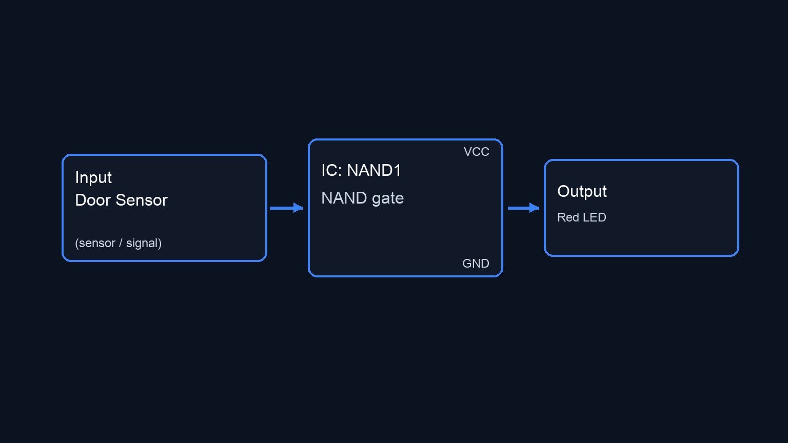
Schematic
VCC --> [ SW1: Door Sensor ] --+--(DOOR)----->+
                               |              |
                         [ R1: 10 kΩ ]         v
                               |        [ U1: NAND1 ] --(NAND_OUT)--> [ U1: NAND2 ] --(ALARM)--> [ R3: 330 Ω ] --(LED_IN)--> [ D1: Red LED ] --> GND
                              GND       [ Pins 1,2->3 ]               [ Pins 4,5->6 ]
                                              ^
                                              |
VCC --> [ SW2: Sys Enable ] ---+--(EN)------->+
                               |
                         [ R2: 10 kΩ ]
                               |
                              GND
Truth table
| DOOR (SW1) | EN (SW2) | NAND_OUT (Pin 3) | ALARM (Pin 6) | LED Status |
|---|---|---|---|---|
| 0 (Low) | 0 (Low) | 1 (High) | 0 (Low) | OFF |
| 0 (Low) | 1 (High) | 1 (High) | 0 (Low) | OFF |
| 1 (High) | 0 (Low) | 1 (High) | 0 (Low) | OFF |
| 1 (High) | 1 (High) | 0 (Low) | 1 (High) | ON (Alarm Active) |
Measurements and tests
- Supply Validation: Measure the voltage between VCC and 0. Ensure it is a stable 5 V.
- Input States: Use a multimeter to measure nodes DOOR and EN with respect to ground (0). Verify they read 0 V when the switch is open and 5 V when the switch is closed.
- Intermediate Logic: Close both SW1 and SW2. Measure node NAND_OUT. It should drop to 0 V (Logic Low) only when both switches are closed.
- Final Output: Measure node ALARM. It should read 5 V (Logic High) only when both switches are closed, confirming that U1B correctly inverted the signal from U1 A.
- Load Check: Verify the voltage drop across D1 is roughly 1.8 V to 2.2 V when illuminated.
SPICE netlist and simulation
Reference SPICE Netlist (ngspice) — excerptFull SPICE netlist (ngspice)
* Practical case: Open door alarm with inhibition
.width out=256

* Main Power Supply
V1 VCC 0 DC 5

* Door Sensor (SW1) - Modeled as a voltage-controlled switch with a pulse source
V_ctrl1 ctrl1 0 PULSE(0 5 0 1u 1u 50u 100u)
S1 VCC DOOR ctrl1 0 mySW
R1 DOOR 0 10k

* System Enable (SW2) - Modeled as a voltage-controlled switch with a slower pulse source
V_ctrl2 ctrl2 0 PULSE(0 5 0 1u 1u 100u 200u)
S2 VCC EN ctrl2 0 mySW
R2 EN 0 10k

* 74HC00 Quad 2-input NAND gate
* Wiring: 1->DOOR, 2->EN, 3->NAND_OUT, 4->NAND_OUT, 5->NAND_OUT, 6->ALARM, 7->0, 14->VCC
XU1 DOOR EN NAND_OUT NAND_OUT NAND_OUT ALARM 0 VCC 74HC00

* ... (truncated in public view) ...
Copy this content into a .cir file and run with ngspice.
* Practical case: Open door alarm with inhibition
.width out=256

* Main Power Supply
V1 VCC 0 DC 5

* Door Sensor (SW1) - Modeled as a voltage-controlled switch with a pulse source
V_ctrl1 ctrl1 0 PULSE(0 5 0 1u 1u 50u 100u)
S1 VCC DOOR ctrl1 0 mySW
R1 DOOR 0 10k

* System Enable (SW2) - Modeled as a voltage-controlled switch with a slower pulse source
V_ctrl2 ctrl2 0 PULSE(0 5 0 1u 1u 100u 200u)
S2 VCC EN ctrl2 0 mySW
R2 EN 0 10k

* 74HC00 Quad 2-input NAND gate
* Wiring: 1->DOOR, 2->EN, 3->NAND_OUT, 4->NAND_OUT, 5->NAND_OUT, 6->ALARM, 7->0, 14->VCC
XU1 DOOR EN NAND_OUT NAND_OUT NAND_OUT ALARM 0 VCC 74HC00

* Alarm LED indicator
R3 ALARM LED_IN 330
D1 LED_IN 0 DLED

* Models and Subcircuits
.model mySW SW(Ron=1 Roff=100Meg Vt=2.5)
.model DLED D(IS=1e-15 N=2 RS=10)

* 74HC00 Subcircuit implementation (using robust continuous B-sources for logic)
.subckt 74HC00 1 2 3 4 5 6 7 14
* Gate 1 (Pins 1, 2 -> 3)
B1 3 7 V = 5 * (1 - (1 / (1 + exp(-50*(V(1,7)-2.5)))) * (1 / (1 + exp(-50*(V(2,7)-2.5)))))
* Gate 2 (Pins 4, 5 -> 6)
B2 6 7 V = 5 * (1 - (1 / (1 + exp(-50*(V(4,7)-2.5)))) * (1 / (1 + exp(-50*(V(5,7)-2.5)))))
* Dummy loads to prevent floating pins
R1 1 7 100Meg
R2 2 7 100Meg
R3 4 7 100Meg
R4 5 7 100Meg
R5 14 7 100Meg
.ends

* Analysis Directives
.op
.tran 1u 300u
.print tran V(DOOR) V(EN) V(ALARM) V(LED_IN)
.end
Simulation Results (Transient Analysis)

Show raw data table (412 rows)
Index   time            v(door)         v(en)           v(alarm)        v(led_in)
0	0.000000e+00	4.999000e-04	4.999000e-04	-7.41841e-68	4.091162e-30
1	1.000000e-08	4.999000e-04	4.999000e-04	-7.41841e-68	2.688961e-41
2	2.000000e-08	4.999000e-04	4.999000e-04	-7.41841e-68	-2.68896e-41
3	4.000000e-08	4.999000e-04	4.999000e-04	-7.41841e-68	-8.83675e-52
4	8.000000e-08	4.999000e-04	4.999000e-04	-7.41841e-68	3.534698e-52
5	1.600000e-07	4.999000e-04	4.999000e-04	-7.41841e-68	1.858568e-62
6	3.200000e-07	4.999000e-04	4.999000e-04	-7.41841e-68	-4.64651e-63
7	3.562500e-07	4.999000e-04	4.999000e-04	-7.41841e-68	-7.41842e-68
8	4.196875e-07	4.999000e-04	4.999000e-04	-7.41841e-68	-7.41841e-68
9	4.372461e-07	4.999000e-04	4.999000e-04	-7.41841e-68	-7.41841e-68
10	4.679736e-07	4.999000e-04	4.999000e-04	-7.41841e-68	-7.41841e-68
11	5.019934e-07	4.999500e+00	4.999500e+00	5.000000e+00	1.651140e+00
12	5.700330e-07	4.999500e+00	4.999500e+00	5.000000e+00	1.651062e+00
13	7.061121e-07	4.999500e+00	4.999500e+00	5.000000e+00	1.650721e+00
14	9.782703e-07	4.999500e+00	4.999500e+00	5.000000e+00	1.650725e+00
15	1.000000e-06	4.999500e+00	4.999500e+00	5.000000e+00	1.650721e+00
16	1.043459e-06	4.999500e+00	4.999500e+00	5.000000e+00	1.650721e+00
17	1.130378e-06	4.999500e+00	4.999500e+00	5.000000e+00	1.650721e+00
18	1.304216e-06	4.999500e+00	4.999500e+00	5.000000e+00	1.650721e+00
19	1.651892e-06	4.999500e+00	4.999500e+00	5.000000e+00	1.650721e+00
20	2.347244e-06	4.999500e+00	4.999500e+00	5.000000e+00	1.650721e+00
21	3.347244e-06	4.999500e+00	4.999500e+00	5.000000e+00	1.650721e+00
22	4.347244e-06	4.999500e+00	4.999500e+00	5.000000e+00	1.650721e+00
23	5.347244e-06	4.999500e+00	4.999500e+00	5.000000e+00	1.650721e+00
... (388 more rows) ...
Reference SPICE netlist (ngspice)
* Practical case: Open door alarm with inhibition
.width out=256

* Main Power Supply
V1 VCC 0 DC 5

* Door Sensor (SW1) - Modeled as a voltage-controlled switch with a pulse source
V_ctrl1 ctrl1 0 PULSE(0 5 0 1u 1u 50u 100u)
S1 VCC DOOR ctrl1 0 mySW
R1 DOOR 0 10k

* System Enable (SW2) - Modeled as a voltage-controlled switch with a slower pulse source
V_ctrl2 ctrl2 0 PULSE(0 5 0 1u 1u 100u 200u)
S2 VCC EN ctrl2 0 mySW
R2 EN 0 10k

* 74HC00 Quad 2-input NAND gate
* Wiring: 1->DOOR, 2->EN, 3->NAND_OUT, 4->NAND_OUT, 5->NAND_OUT, 6->ALARM, 7->0, 14->VCC
XU1 DOOR EN NAND_OUT NAND_OUT NAND_OUT ALARM 0 VCC 74HC00

* Alarm LED indicator
R3 ALARM LED_IN 330
D1 LED_IN 0 DLED

* Models and Subcircuits
.model mySW SW(Ron=1 Roff=100Meg Vt=2.5)
.model DLED D(IS=1e-15 N=2 RS=10)

* 74HC00 Subcircuit implementation (using robust continuous B-sources for logic)
.subckt 74HC00 1 2 3 4 5 6 7 14
* Gate 1 (Pins 1, 2 -> 3)
B1 3 7 V = 5 * (1 - (1 / (1 + exp(-50*(V(1,7)-2.5)))) * (1 / (1 + exp(-50*(V(2,7)-2.5)))))
* Gate 2 (Pins 4, 5 -> 6)
B2 6 7 V = 5 * (1 - (1 / (1 + exp(-50*(V(4,7)-2.5)))) * (1 / (1 + exp(-50*(V(5,7)-2.5)))))
* Dummy loads to prevent floating pins
R1 1 7 100Meg
R2 2 7 100Meg
R3 4 7 100Meg
R4 5 7 100Meg
R5 14 7 100Meg
.ends

* Analysis Directives
.op
.tran 1u 300u
.print tran V(DOOR) V(EN) V(ALARM) V(LED_IN)
.end
Simulation Results (Transient Analysis)
Common mistakes and how to avoid them
- Floating CMOS inputs: Forgetting the pull-down resistors (R1, R2) will leave the inputs floating when the switches are open, causing unpredictable LED blinking and excessive IC current draw. Always ensure mechanical switches are paired with pull-up or pull-down resistors.
- Leaving unused gates floating: The 74HC00 contains four gates. Leaving the inputs of gates 3 and 4 disconnected can cause high-frequency oscillations. Tie pins 8, 9, 12, and 13 to ground (0).
- Misunderstanding NAND logic for NOT: To use a NAND gate as an inverter (NOT gate), you must tie both inputs together (as done on pins 4 and 5). Supplying the signal to only one pin while leaving the other floating will result in faulty logic.
Troubleshooting
- Symptom: The LED never turns on.
- Cause: D1 might be inserted backward (reverse polarity), or R3 is too large.
- Fix: Check that the long leg (anode) of D1 faces ALARM and the flat side (cathode) goes to 0. Verify R3 is 330 Ω, not 330 kΩ.
- Symptom: The LED turns on as soon as one switch is closed, ignoring the other.
- Cause: A wiring error on the 74HC00 inputs, or an input pin is shorted to VCC.
- Fix: Check continuity on pins 1 and 2. Ensure they are isolated from each other and correctly routed to DOOR and EN.
- Symptom: The circuit is highly sensitive to hand movements nearby.
- Cause: Floating inputs. The pull-down resistors are either disconnected or not making good contact on the breadboard.
- Fix: Verify R1 and R2 are securely connected between the switch signal nodes and ground.
Possible improvements and extensions
- Active Buzzer Integration: Add a 5 V active buzzer in parallel with the LED (and its resistor) so the alarm provides both visual and auditory feedback.
- Flashing Alarm: Use the two remaining NAND gates in the 74HC00 along with a resistor and capacitor to build an astable multivibrator, making the LED blink repeatedly when the alarm is triggered instead of staying solid.
More Practical Cases on Prometeo.blog
Find this product and/or books on this topic on Amazon
As an Amazon Associate, I earn from qualifying purchases. If you buy through this link, you help keep this project running.
Quick Quiz

Telecommunications Electronics Engineer and Computer Engineer (official degrees in Spain).